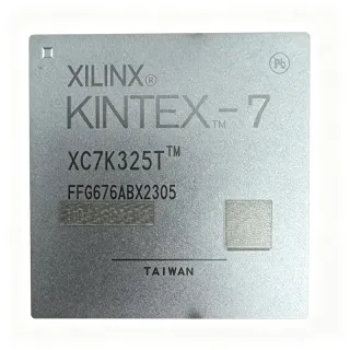
XC5VLX50-2FFG676C - 46,080-Cell Virtex-5 LX FPGA | AMD
부품 번호: XC5VLX50-2FFG676C ✗ 단종XC5VLX50-2FFG676C 개요
A field-programmable gate array is a semiconductor device whose internal digital logic, interconnect, and I/O behavior are configured after manufacture. In the product hierarchy, an FPGA is a programmable-logic device, a flexible alternative to a fixed-function application-specific integrated circuit. The Virtex-5 LX family combines configurable logic blocks, block RAM, dedicated hard processors, and high-speed transceiver resources, allowing one package to implement parallel processing, interface bridging, signal transformation, and embedded control functions.
The principal device characteristics include 46,080 logic cells, 3,600 configurable logic blocks, 440 I/O, a 1 V core voltage, and 65 nm CMOS fabrication. These resources distinguish XC5VLX50 from smaller Virtex-5 members and from the M2GL family listed in the industrial design ecosystem. The 440 available I/O also support direct connection to external memory, high-speed transceivers, parallel buses, and mixed-signal interface circuits when their electrical requirements are compatible.
The second-generation ASMBL column-based architecture separates the FPGA into configurable logic and routing columns. This structure allows logic functions to be distributed across the device while programmable switch matrices interconnect them. Dedicated resources support memory-intensive and serial designs, but exact block counts, serializer rates, transceiver counts, and performance specifications should be confirmed in the Virtex-5 LX documentation for the exact device and package combination.
XC5VLX50-2FFG676C is suited to industrial control, telecommunications, networking, test and measurement, video processing, and embedded signal-processing systems. The 676-ball FCBGA package supports dense board-level interconnect and is appropriate for multilayer PCB designs where routing density and electrical performance are important. The device can also form the central programmable element of a larger system containing memory, clocking, power-management circuitry, transceivers, and external data-conversion components.
Board design requires careful attention to the recommended VCCINT, VCCAUX, and VCCO power-on sequence because the manufacturer does not specify minimum current for unsupported sequences. Decoupling, simultaneous switching-noise control, clock integrity, and the 676-ball escape-routing strategy are equally important. Use the official package pinout files and board-design guidance when assigning every power, ground, configuration, and user I/O connection.
This product summary combines device identification, package characteristics, architectural context, sourcing guidance, and practical implementation considerations. It is designed to help engineers evaluate the XC5VLX50-2FFG676C quickly while still directing critical footprint, power, pinout, and timing decisions back to the manufacturer documentation.
드롭인 대체품: XC5VLX50-2FFG676C — 동일 패키지, 핀 호환. PCB 재작업이 필요한 다른 패키지 부품은 제외됩니다.
이 시리즈의 변형
다음과 드롭인 호환되는 동일 시리즈 모델: XC5VLX50-2FFG676C (동일 폼 팩터 및 풋프린트) — 차이점: Device Type, Speed Grade, Temperature Grade, Package, Architecture.
XC5VLX50-1FFG676C
✅ 드롭인가격 문의
데이터시트 보기 →XC5VLX50-1FFG676I
✅ 드롭인가격 문의
데이터시트 보기 →XC5VLX50-2FF676I
✅ 드롭인가격 문의
데이터시트 보기 →XC5VLX50-2FF676C
✅ 드롭인가격 문의
데이터시트 보기 →XC5VLX50-2FFG676C 최대 정격 & 전기적 특성
| Device Family | Virtex-5 LX |
| Device Type | Field-Programmable Gate Array (FPGA) |
| Logic Cells | 46,080 cells |
| Configurable Logic Blocks | 3,600 CLBs |
| User I/O Count | 440 I/O |
| Process Technology | 65 nm CMOS |
| Core Supply Voltage | 1 V |
| Performance Grade | -2 speed grade |
| Temperature Grade | C commercial grade |
| 패키지 | 676-BBGA, FCBGA |
| Package Pin Count | 676 pins |
| 실장 유형 | Surface Mount |
| Architecture | Second-generation ASMBL column-based architecture |
| Recommended Power-On Sequence | VCCINT, VCCAUX, then VCCO |
XC5VLX50-2FFG676C 676 pins 핀 구성 가이드
XC5VLX50-2FFG676C(676 pins 패키지)의 핀 구성입니다. 이 디지털 IC에는 GPIO, 통신 인터페이스(UART, SPI, I2C), 전원 핀이 포함되어 있습니다. 대체 핀 기능과 구성 옵션은 제조사 데이터시트를 참조하십시오. 임베디드 시스템 설계와 PCB 레이아웃에 필수적입니다.

다음에 대한 상세 핀아웃 데이터 없음: XC5VLX50-2FFG676C.
다음을 참조하십시오: 데이터시트 전체 핀 구성은 다음을 참조하십시오.
일반적인 애플리케이션
XC5VLX50-2FFG676C 적합 용도: 6 애플리케이션s: Industrial Control and Automation, Telecommunications Network Equipment, High-Speed Data Acquisition, Video and Image Processing, Test and Measurement Systems, Embedded Signal Processing.
Industrial Control and Automation
XC5VLX50-2FFG676C fits centralized industrial controllers that must combine deterministic parallel logic with numerous field-bus, digital I/O, and communication interfaces. Its 46,080 logic cells and 3,600 configurable logic blocks provide substantial programmable capacity, while 440 user I/O simplify connections to sensors, actuators, fieldbus transceivers, and industrial processors. The -2 performance grade can provide additional timing margin for demanding control loops. The primary design consideration is preserving a clean power and clock environment because 440 external connections increase routing, return-current, and simultaneous-switching-noise sensitivity.
Telecommunications Network Equipment
XC5VLX50-2FFG676C is appropriate for telecommunications equipment requiring parallel packet processing, protocol adaptation, traffic management, and extensive backplane connectivity. The device's 46,080 logic cells can support parallel lanes, lookup functions, switching fabrics, and test instrumentation, while the 676-ball FCBGA package offers dense interconnect for multilayer boards. Its 440 I/O allow direct attachment to network transceivers and parallel bus structures. Engineers should use the Virtex-5 power-sequence and pinout documentation to control VCCINT, VCCAUX, and VCCO behavior and should carefully manage simultaneous output switching.
High-Speed Data Acquisition
XC5VLX50-2FFG676C can serve as the programmable acquisition engine in a data-collection system that combines multiple parallel sensors, counters, digital filtering, and host-interface logic. Its 3,600 CLBs and 440 I/O allow several acquisition channels and timing functions to be integrated without relying on multiple fixed-function controllers. The -2 grade provides additional performance margin for parallel processing, while the large package supports a high pin count on multilayer PCBs. Signal-integrity planning is essential: controlled-impedance routing, solid ground planes, terminated inputs, and separate clock distribution should be used to limit data errors.
Video and Image Processing
XC5VLX50-2FFG676C suits programmable video pipelines that must perform parallel pixel manipulation, filtering, format conversion, or test-pattern generation. The 46,080-cell Virtex-5 LX device provides enough parallel resources for wide data paths, while 440 I/O support high-volume connections to external memory and video interfaces. Its -2 performance grade helps preserve timing margin in wide datapaths, although final throughput depends on the selected clock, I/O standards, and board-level constraints. Because the FCBGA package has 676 balls, designers should plan escape routing, reference planes, decoupling, and simultaneous-switching-noise mitigation before layout release.
Test and Measurement Systems
XC5VLX50-2FFG676C can implement configurable logic, pattern generation, acquisition control, and analysis pipelines in sophisticated test and measurement equipment. Its large I/O count permits connections to instruments, memory, and programmable test interfaces, while 46,080 logic cells support parallel algorithms and timing checks. The -2 grade offers additional implementation margin for complex sequential logic and high-speed interfaces. The device is particularly suitable when one platform must support multiple test modes through reconfiguration. Designers should isolate sensitive analog and reference circuitry from FPGA power domains and verify thermal behavior under sustained high switching activity.
Embedded Signal Processing
XC5VLX50-2FFG676C supports embedded signal-processing systems that combine filtering, correlation, spectral processing, packet parsing, and control in one programmable device. The combination of 3,600 CLBs, dedicated Virtex-5 resources, and 440 user I/O permits concurrent datapaths with flexible external connectivity. Its -2 grade can improve timing closure for parallel pipelines, while the 676-ball package supports a compact but routing-intensive board layout. Power budgeting, clock jitter, and I/O standard selection remain central design constraints. Use the manufacturer power table and package pinout files to implement the recommended VCCINT, VCCAUX, and VCCO sequence correctly.
엔지니어링 참조 데이터: XC5VLX50-2FFG676C — 비교, 설계 지침 및 규정 준수 정보.
선택 가이드
대체품과의 비교
| 파라미터 | 이 제품 | XC5VLX50-1FFG676C | XC5VLX50-1FFG676I | XC5VLX50-2FF676I | XC5VLX50-2FF676C |
|---|---|---|---|---|---|
| Brand | AMD | AMD | AMD | AMD | AMD |
| Package | 676-BBGA, FCBGA | 676-BBGA, FCBGA - same | 676-BBGA, FCBGA - same | 676-BBGA, FCBGA - same | 676-BBGA, FCBGA - same |
| Device Family | Virtex-5 LX | Virtex-5 LX | Virtex-5 LX | Virtex-5 LX | Virtex-5 LX |
| Logic Cells | 46,080 cells | 46,080 cells | 46,080 cells | 46,080 cells | 46,080 cells |
| Configurable Logic Blocks | 3,600 CLBs | 3,600 CLBs | 3,600 CLBs | 3,600 CLBs | 3,600 CLBs |
| User I/O | 440 I/O | 440 I/O | 440 I/O | 440 I/O | 440 I/O |
| Performance Grade | -2 | -1 | -1 | -2 | -2 |
| Temperature Grade | C commercial grade | C commercial grade | I industrial grade | I industrial grade | C commercial grade |
| Process Technology | 65 nm CMOS | 65 nm CMOS | 65 nm CMOS | 65 nm CMOS | 65 nm CMOS |
| Core Supply Voltage | 1 V | 1 V | 1 V | 1 V | 1 V |
주요 차별점
- Higher performance grade within the same device configuration (vs XC5VLX50-1FFG676C)
- Commercial temperature ordering option (vs XC5VLX50-2FF676I)
- Identical large FPGA resource organization across documented variants (vs XC5VLX50-2FF676C)
설계 노트
Implement the documented VCCINT, VCCAUX, and VCCO power-on sequence because the manufacturer's minimum-current table applies only to that ordering. Place the required bulk and bypass capacitors at their associated supply balls, keep the high-current return path within the power plane, and use separate regulator paths where sequencing requires independent control. Validate startup with the production power supply because rail ramp rates and load transients can affect configuration behavior.
The 676-ball FCBGA requires multilayer escape routing and a pin-aware fanout before functional routing begins. Use the manufacturer package pinout file to classify power, ground, configuration, clock-capable, and user I/O balls. Preserve uninterrupted reference planes beneath the device, avoid splits across the BGA array, and maintain short return paths for high-speed and high-switching nets. Run package and board-rule checks after every major placement or routing revision.
Do not substitute a different speed or temperature suffix without checking the design requirements. XC5VLX50-1FFG676C changes performance grade, XC5VLX50-1FFG676I changes both performance and temperature grade, and XC5VLX50-2FF676I changes temperature grade. The 676-ball package alone does not establish interchangeability. Confirm timing margins, environmental limits, pin assignments, configuration requirements, and device markings before approving a replacement.
With 440 user I/O and a large external-pin count, simultaneous switching noise and clock-distribution quality can materially affect performance. Use a solid ground reference, matched-length rules for critical buses, controlled-impedance routing, and receiver termination where required. Isolate clocks from high-fanout data nets, keep configuration and JTAG routing away from noisy interfaces, and verify edge quality and timing at the production I/O voltage and temperature extremes.
규정 준수 정보
A RoHS non-compliant and lead-containing status was reported for the related XC5VLX50-2FF676C ordering code, but the exact G-suffix target could not be classified from the manufacturer documentation. The exact XC5VLX50-2FFG676C compliance status requires confirmation from AMD or the authorized supply channel.