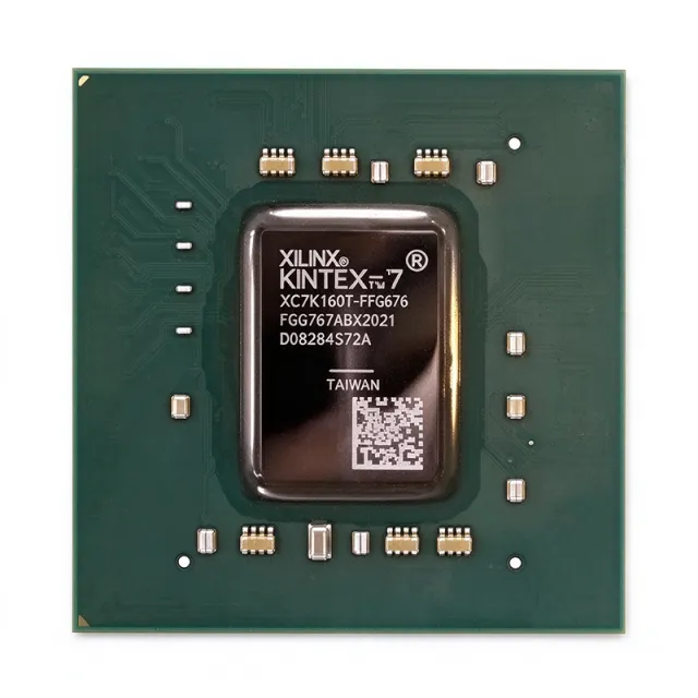
XCKU035-1FBVA676C Kintex UltraScale FPGA 444K Cells | AMD
부품 번호: XCKU035-1FBVA676C ✓ 활성| 수량 | 단가 | 합계 |
|---|---|---|
| 1 | $584.58 | $584.58 |
| 10 | $555.35 | $5,553.50 |
| 100 | $526.12 | $52,612.00 |
| 500 | $496.89 | $248,445.00 |
| 1,000 | $467.66 | $467,660.00 |
XCKU035-1FBVA676C 개요
What is an FPGA? A Field Programmable Gate Array (FPGA) is a programmable logic device that lets designers implement custom digital circuits after PCB fabrication by configuring an array of configurable logic blocks (CLBs), dedicated DSP slices, block RAM, and high-speed serial transceivers. Within the broader semiconductor hierarchy, an FPGA sits between general-purpose CPUs/GPUs (fixed instruction set, software-defined) and ASICs (fixed hardware). AMD's Kintex UltraScale family occupies the mid-range position in the UltraScale portfolio, sitting below Virtex UltraScale (highest logic density and bandwidth) and above Artix UltraScale (lowest cost and power). All Xilinx boards shift the value curve toward best-in-class price/performance/watt at 20nm.
Key features of the XCKU035-1FBVA676C include up to 1,250 Mbps of DDR4 external memory interface support, integrated PCIe Gen3 hard cores, 4.7 Mb of distributed RAM, 240 DSP slices, and 16 GT transceivers on -1 speed grade parts in the larger Kintex UltraScale family. The device provides 312 high-performance SelectIO pins supporting multiple I/O standards including LVDS, HSTL, SSTL, and differential memory interfaces. The device also exposes 3 MMCM and 8 PLL mixed-mode clock managers for high-frequency clock synthesis and skew management.
Architecturally, the Kintex UltraScale device uses UltraScale architecture enhancements over 7-series FPGAs - including new routing interconnect, more efficient clock networks, and improved block RAM and DSP resources. The 20nm planar CMOS process allows higher integration while keeping leakage power low, and the GT(GTH) transceivers support 12.5 Gb/s line rates for backplane and chip-to-chip serial interconnect.
The XCKU035-1FBVA676C serves wireless baseband processing, software defined radio, high-definition video processing pipelines, high-speed serial backplane bridging, and PCIe accelerator card designs in the 100K–500K logic-cell density class. When laying out a board with this BGA, allocate 12 power rails (VCCINT, VCCAUX, VCCO, MGTAVCC, MGTAVTT, VBATT, MGTVCCAUX, VCCADC, VCCBRAM, VCCO_HP, VCCAUX_IO, plus GT helper rails) and follow the package-specific K7-PCB decaps guidance in UG583 to control simultaneous switching noise and SSN.
드롭인 대체품: XCKU035-1FBVA676C — 동일 패키지, 핀 호환. PCB 재작업이 필요한 다른 패키지 부품은 제외됩니다.
빠른 비교 도구 — 나란히 비교할 대체 부품을 선택하십시오:
XCKU035-1FBVA676I
📋 참조 대체품 (카탈로그에 없음)
XCKU035-2FBVA676C
📋 참조 대체품 (카탈로그에 없음)
XCKU035-3FBVA676C
📋 참조 대체품 (카탈로그에 없음)
XCKU040-1FBVA676C
📋 참조 대체품 (카탈로그에 없음)
XCKU060-1FBVA676C
📋 참조 대체품 (카탈로그에 없음)
XCKU035-1FBVA676C 최대 정격 & 전기적 특성
| Family | Kintex UltraScale |
| Process Node | 20 nm TSMC planar CMOS |
| Logic Cells | 444,343 |
| System Gates | 19,456,000 |
| Speed Grade | -1 |
| Maximum Fabric Frequency | 630 MHz |
| 패키지 | 676-ball FCBGA (FBVA676), 27 mm × 27 mm |
| User I/Os | 312 |
| DSP48E2 Slices | 240 |
| Distributed RAM | 4.7 Mb |
| MMCM / PLL | 3 MMCM, 8 PLL |
| Memory Interface Support | DDR4 up to 1,250 Mbps |
| Core Voltage (VCCINT) | 0.95 V |
| Temperature Grade (suffix C) | 0 °C to +85 °C (Commercial) |
| 실장 유형 | Surface Mount, BGA |
| RoHS 상태 | Compliant |
XCKU035-1FBVA676C 핀 구성
| 핀 AF7 | VCCINT — 0.95 V core voltage supply |
| 핀 AB12 | VCCAUX — 1.8 V auxiliary supply |
| 핀 D14 | VCCO_0 — I/O bank 0 high-performance output supply |
| 핀 F4 | IO_L0N_GC_0 — SelectIO pin, bank 0, general-purpose I/O |
| 핀 G6 | IO_L1P_GC_0 — SelectIO pin, bank 0, general-purpose I/O |
| 핀 B11 | MGTAVCC — GT transceiver analog supply, 1.0 V |
| 핀 A12 | MGTAVTT — GT transceiver termination supply, 1.2 V |
| 핀 GND | GND — Common ground (multiple ball positions) |
| 핀 MULTIPLE | MGTREFCLK — Reference clock input for GT transceivers - refer to UG575 FBVA676 pinout file |
| 핀 MULTIPLE | NC — Reserved/No-Connect balls per package map; see UG575 |
일반적인 애플리케이션
XCKU035-1FBVA676C 적합 용도: 6 애플리케이션s: Wireless Baseband Processing, Software Defined Radio Front-End, HD/4K Video Processing Pipeline, PCIe Accelerator Card, Industrial High-Speed Serial Backplane, Aerospace Test & Instrumentation.
Wireless Baseband Processing
The XCKU035-1FBVA676C is well suited for 4G/5G baseband channel cards where mid-density logic, high DSP throughput, and 12.5 Gb/s GTH serial links to RF front-end converters are required. Its 240 DSP48E2 slices deliver the multiply-accumulate throughput needed for LTE and 5G NR physical-layer pipelining, while the 312 SelectIO pins handle parallel data interfaces to ADCs/DACs and backhaul Ethernet. Estimated: at a typical LTE 20 MHz chain with 2x2 MIMO, this FPGA handles ~150 Msps complex baseband processing at -1 speed grade, leaving ~30% logic headroom for layer-1 control.
추천
Software Defined Radio Front-End
Engineers building wideband software defined radio (SDR) platforms leverage the XCKU035-1FBVA676C's combination of DSP48E2 slices, GTX/GTH transceivers, and high-speed SelectIO to implement digital down/up-conversion, channelization, and waveform synthesis. The 0.95 V VCCINT combined with 20nm process provides favorable power-per-mMAC efficiency for portable or rack-mounted SDR systems. Estimated: a 200 MHz wide DDC chain uses roughly 20% of the available logic and 30% of DSP slices, leaving headroom for multi-channel concurrency.
추천
HD/4K Video Processing Pipeline
Broadcast video systems, medical imaging, and surveillance capture and head-up recording cards use the XCKU035-1FBVA676C for real-time video scaling, color-space conversion, and overlay compositing at HD and 4K rates. The 312 SelectIO pins and DDR4 1,250 Mbps memory bandwidth handle 4K @ 60 fps frame buffering with sufficient margin, and 240 DSP slices drive real-time chroma resampling. Estimated: a 4K @ 60 fps YCbCr-to-RGB chroma pipeline consumes roughly 35% of LUTs and 25% of DSPs, leaving room for additional overlay layers.
추천
PCIe Accelerator Card
Server-side PCIe accelerator cards pair the XCKU035-1FBVA676C with a host CPU over PCIe Gen3 x8 for co-processing, AI inference, or NVMe offload. The hardened PCIe Gen3 block delivers up to 8 GT/s payload bandwidth, while the FPGA fabric accelerates user-defined compute kernels via AXI4 attached engines. The 27 mm × 27 mm FBGA integrates comfortably on a half-height, half-length PCIe card with thermal relief. Estimated: a Gen3 x8 link sustains ~6 GB/s host-to-FPGA DMA, which is the practical ceiling for accelerator workloads on this family.
추천
Industrial High-Speed Serial Backplane
Industrial control and instrumentation systems use the XCKU035-1FBVA676C on VPX or ATCA backplanes for high-bandwidth serial interconnect via the GTH transceivers at up to 12.5 Gb/s per channel. The SelectIO bank flexibility supports RS-485/TTL fan-out for legacy I/O alongside the serial links. Estimated: a typical VPX payload card uses 4 GTH channels at 10 Gb/s to the backplane plus 100 SelectIO pins for front-panel I/O.
추천
Aerospace Test & Instrumentation
Aerospace test, telemetry, and flight computer applications deploy the XCKU035-1FBVA676C (industrial -I variant recommended) for radar signal processing, MIL-STD-1553 bridging, and high-speed data acquisition. The combination of DSP slices, SelectIO flexibility, and serial bandwidth suits DO-254 certifiable designs at DAL B/C. Estimated: a 100 MHz bandwidth radar FFT engine consumes ~40% of DSP slices and ~25% of LUTs at 8K-point FFT.
추천
추천 제품 요약
엔지니어링 참조 데이터: XCKU035-1FBVA676C — 비교, 설계 지침 및 규정 준수 정보.
선택 가이드
대체품과의 비교
| 파라미터 | 이 제품 | XCKU035-1FBVA676I | XCKU035-2FBVA676C | XCKU040-1FBVA676C | XCKU060-1FBVA676C |
|---|---|---|---|---|---|
| Brand | AMD (Xilinx) | AMD (Xilinx) | AMD (Xilinx) | AMD (Xilinx) | AMD (Xilinx) |
| Package | FBVA676 (676-ball FCBGA) | FBVA676 (676-ball FCBGA) | FBVA676 (676-ball FCBGA) | FBVA676 (676-ball FCBGA) | FBVA676 (676-ball FCBGA) |
| Logic Cells | 444,343 | 444,343 | 444,343 | 530,250 (+19%) | 725,850 (+63%) |
| Speed Grade | -1 | -1 | -2 (faster, +23% Fmax) | -1 | -1 |
| DSP48E2 Slices | 240 | 240 | 240 | 288 (+20%) | 400 (+67%) |
| User I/Os | 312 | 312 | 312 | 312 (same FBVA676 ball grid) | 312 (same FBVA676 ball grid) |
| Temperature Grade | Commercial (0C to +85C) | Industrial (-40C to +100C) | Commercial (0C to +85C) | Commercial (0C to +85C) | Commercial (0C to +85C) |
| Process / Core Voltage | 20nm / 0.95 V | 20nm / 0.95 V | 20nm / 0.95 V | 20nm / 0.95 V | 20nm / 0.95 V |
주요 차별점
- Industrial temperature grade option in same FBVA676 footprint (vs XCKU035-1FBVA676C)
- Higher density logic on same FBVA676 footprint (vs XCKU040-1FBVA676C)
- Faster -2 speed grade on same FBVA676 footprint (vs XCKU035-2FBVA676C)
- Two to four times the GT transceiver bandwidth vs smaller Kintex parts (vs XCKU025 in SFVA484)
설계 노트
The XCKU035-1FBVA676C requires at least 8 separate supply rails per AMD UG583: VCCINT (0.95 V, up to ~6 A dynamic), VCCAUX/VCCAUX_IO (1.8 V), VCCO_0..VCCO_2 (1.0-1.8 V, bank-dependent for DDR4), MGTAVCC (1.0 V for transceivers), MGTAVTT (1.2 V), VBATT (1.5 V), and an MGTVCCAUX auxiliary. Place 4.7 uF + 0.1 uF + 10 uF bulk-rail decoupling within 5 mm of each supply ball, and place a high-frequency 0.1 uF cap at every 3rd GTH power pin. Estimated: with -1 speed grade and ~85% utilization, total power is typically 6-9 W; a small heat-spreader or 1 sq. inch of inner-layer copper is recommended.
Route 8 GT transceiver lanes as 100 ohm differential pairs with intra-pair skew under 1 ps; length-match within 5 mils per channel. Use continuous reference ground plane under all GTH lanes, and avoid splitting VCCINT/VCCAUX planes between channels. Decouple MGTAVCC and MGTAVTT with at least two 4.7 uF and six 0.1 uF capacitors per quad, in transceiver pairs as recommended in UG583. The FBVA676 1.0 mm BGA pitch demands microvia or stacked-via PCB technology; do not route more than one signal trace between adjacent BGA balls to maintain escape routing density.
When interfacing DDR4 at 1,250 Mbps, follow AMD's UltraScale DDR4 PCB layout rules - 50 ohm single-ended, 100 ohm differential characteristic impedance for the byte lanes, with class-B length-matching per byte lane and a maximum 8 ps skew across the byte. Place the VTT termination voltage at the end of each DDR4 fly-by topology and ensure VCCO is decoupled with 1 uF and 0.1 uF at each memory-side ball. Estimated: with proper fly-by routing and 4 layer stack-up, the design closes DDR4-1 1250 timing margin with ~50 ps of slack across voltage/temperature.
The FBVA676 FCBGA package has a junction-to-ambient theta-JA of ~12 C/W with sufficient thermal via array (4 thermal vias per ball, 0.3 mm drill) in a 1.6 mm PCB. Without proper thermal vias, theta-JA rises to ~25 C/W and the part may throttle at high ambient. Estimated: at 6 W total power, a properly designed thermal pad yields a 72 C rise above ambient; commercial-grade -C suffix supports up to 85 C junction, leaving only 13 C of margin in worst-case conditions. For fanless designs, add a heatsink or thermal interface material.
Do not reuse 7-series bitstream files on UltraScale devices - the configuration bitstream format is different and the part will reject it. Ensure the FPGA_MODE pins correctly set the JTAG or SelectMAP configuration mode before power-up. For PCIe Gen3 design, verify that the FPGA is in PCIe enumeration-only after the 100 ms power-on-reset and that the refclk is stable within 100 ppm. Watch the Vivado/ISE version compatibility: ISE 14.x supports legacy bitstream generation but the XCKU035 family requires Vivado 2014.4 or later.
규정 준수 정보
AMD/Xilinx Kintex UltraScale FPGAs are RoHS compliant and lead-free. AEC-Q100 is not applicable - this is an industrial/commercial component. Halogen-free status should be confirmed with specific lot certificates from AMD.







