Produk (44,000+)

TLV2332ID - Dual 8V 525kHz Operational Amplifier | Texas Instruments
TLV2332ID

TLV2332ID - Dual 8V 525kHz Operational Amplifier | Texas Instruments

The Texas Instruments TLV2332ID is a dual, low-voltage operational amplifier with an 8 V maximum supply rating, 525 kHz gain-bandwidth product, and an 8-pin SOIC package. It is designed for single-supply operation at 3 V and 5 V, providing two amplifier channels in one package. Its common-mode input range extends below the negative supply rail, making it useful in compact systems where signal inputs can approach ground. An operational amplifier is an analog integrated circuit that amplifies the voltage difference between its inverting and non-inverting inputs. The TLV2332 belongs to the LinCMOS low-voltage, medium-power operational-amplifier family. In the broader component hierarchy, it is an operational amplifier, analog amplifier IC, and semiconductor designed for signal conditioning, buffering, voltage comparison, and feedback control. The TLV2332 family is specified for operation from a single supply as low as 3 V and is fully characterized at 5 V and 8 V. Its 525 kHz gain-bandwidth product supports moderate-bandwidth signal paths, while the low input-bias-current characteristics provide low input noise current. The common-mode input voltage can extend below the negative rail, which is particularly helpful for sensor interfaces and single-supply amplifier stages whose useful signal range approaches 0 V. Each device contains two independent amplifier channels. The dual configuration reduces component count and PCB area when a design requires two similar amplifier functions. Because it is a medium-power LinCMOS family member rather than an ultra-low-power comparator or micropower amplifier, it provides a useful balance between bandwidth, low-voltage operation, and drive capability. The exact output-current, input-offset, noise-density, and slew-rate figures should be confirmed in the manufacturer datasheet for the selected operating conditions. Typical uses include low-voltage sensor conditioning, buffered ADC inputs, portable instrumentation, audio preamplification, threshold detection, and general-purpose analog signal processing. The 3 V and 5 V single-supply characterization makes the device suitable for battery-powered and embedded systems, while its 525 kHz bandwidth supports applications that do not require the speed of a high-frequency precision amplifier. PCB design should account for input-bias-current-driven offsets, output drive capability, and stable operation near the supply rails. Place input and output compensation or decoupling components close to their associated pins, maintain short feedback paths, and provide adequate ground-return geometry. Check the datasheet pin configuration and common-mode limits before assigning signal sources, particularly when inputs can remain below 0 V relative to the circuit ground. This product page combines the TLV2332ID device specifications, package details, sourcing guidance, and engineering-oriented design guidance. It also distinguishes documented drop-in choices from unverified substitutions so engineers can assess PCB compatibility, electrical limits, and application fit before approving a replacement.

RFC Hubungi kami
TLV2332IP - Dual 8V 525kHz Op Amp | Texas Instruments
TLV2332IP

TLV2332IP - Dual 8V 525kHz Op Amp | Texas Instruments

The Texas Instruments TLV2332IP is a dual, low-voltage operational amplifier with an 8 V supply rating and 525 kHz gain-bandwidth product, housed in an 8-pin PDIP package. It combines two independent amplifiers with low input bias current in a LinCMOS low-voltage, medium-power design. The dual configuration allows one package to provide two amplifier channels while preserving the supply-voltage and footprint requirements of the TLV233x family. An operational amplifier is an analog signal-processing IC that compares voltages applied to its high-impedance differential inputs and drives an output to reflect their difference. Within the broader semiconductor hierarchy, the TLV2332IP belongs to the operational-amplifier class, then to general-purpose voltage-feedback amplifiers, and finally to linear and mixed-signal integrated circuits. Its differential input stage and high output drive make it suitable for signal conditioning, amplification, filtering, and feedback control. The primary device characteristics include dual-channel operation, an 8 V maximum supply voltage, a 525 kHz gain-bandwidth product, and low input bias current. The low bias current reduces the error introduced when the amplifier is driven by a high-impedance source. Its 525 kHz bandwidth supports applications requiring moderate-frequency closed-loop response without operating as a high-speed precision amplifier. The TLV233x family uses a LinCMOS low-voltage, medium-power architecture intended for single-supply operation. A single-supply configuration means the amplifier can operate with its negative input and supply pins connected to ground while processing signals referenced to a positive rail. This is useful in battery-powered and embedded systems where generating a negative supply would be impractical. Designers should still observe the complete power-supply and common-mode limits in the manufacturer datasheet. Typical applications include sensor-signal conditioning, low-frequency active filters, audio preamplification, general-purpose buffer stages, and embedded analog signal chains. Its dual-channel layout can simplify boards requiring two modest-bandwidth amplification functions, while its PDIP package remains convenient for through-hole prototypes, educational designs, and manually assembled industrial control boards. When using the TLV2332IP, connect the unused amplifier channel to a stable common-mode level close to the configured signal operating point. Confirm the maximum input and output voltage excursions, supply current, output-drive capability, and stability requirements against the manufacturer datasheet before finalizing the circuit. Decoupling capacitors should be placed close to the supply pins to control impedance in the power-distribution network. This product record combines the TLV2332 family specifications, package details, pin assignment, sourcing workflow, and practical selection guidance in one engineering reference. It supports faster design decisions while directing engineers to the manufacturer datasheet for final electrical limits, test conditions, and application-specific validation.

RFC Hubungi kami
TLV2334ID - 4-Channel Low-Power Op Amp | Texas Instruments
TLV2334ID

TLV2334ID - 4-Channel Low-Power Op Amp | Texas Instruments

Texas Instruments TLV2334ID is a four-circuit, general-purpose operational amplifier designed for low-voltage and medium-power applications. The device supports an 8 V maximum supply, 3 V and 5 V single-supply operation, and a common-mode input-voltage range that extends below the negative supply rail. It is packaged in a 14-pin SOIC, making it suitable for conventional analog signal-conditioning boards. An operational amplifier, commonly called an op amp, is an active semiconductor device that uses high-gain differential amplification to improve the gain, input impedance, and output-drive capability of a feedback circuit. Within the broader hierarchy, the TLV2334ID belongs to the operational amplifier, analog amplifier IC, and signal-conditioning IC categories. Its four channels allow compact designs to process multiple independent analog signals without using separate single-amplifier packages. Key characteristics include a 300 kHz gain-bandwidth product, approximately 1.1 mV input offset voltage, four amplifier circuits, and operation from a single 3 V or 5 V supply. The 8 V maximum supply supports low-voltage portable equipment, industrial controls, sensor interfaces, and general-purpose analog conditioning. The common-mode range extending below the negative rail is particularly useful when the signal approaches ground. The TLV2334ID is based on a complementary metal-oxide-semiconductor operational-amplifier design intended for low-voltage operation. Its approximately 300 kHz bandwidth is appropriate for moderate-frequency signal conditioning rather than high-speed video or precision instrumentation. The low-voltage supply capability also simplifies battery-powered designs, although input and output swing limits must be checked against the signal being conditioned. Typical uses include four-channel sensor interfaces, low-voltage audio and control circuits, instrumentation amplifiers, active filters, comparators with added hysteresis, and general-purpose analog buffers. Because the package contains four amplifiers, channel-to-channel matching is useful when several related low-frequency signals must be processed in one circuit. When designing a PCB around the TLV2334ID, place input, output, feedback, and decoupling components close to the relevant pins. Use a local supply bypass capacitor on each supply rail and provide a stable, low-impedance ground return. Check input common-mode voltage and output swing before operating near the supply limits; an amplifier can remain powered while its usable input or output range is restricted. This product page combines the exact catalog attributes and datasheet-search references for the TLV2334ID with practical guidance for supply bypassing, signal conditioning, PCB layout, and drop-in replacement evaluation. It distinguishes confirmed catalog facts from electrical parameters that require review in the manufacturer datasheet before design release.

RFC Hubungi kami
TLV2334IN - 525 kHz Quad CMOS Op Amp | Texas Instruments
TLV2334IN

TLV2334IN - 525 kHz Quad CMOS Op Amp | Texas Instruments

The Texas Instruments TLV2334IN is a quad, general-purpose CMOS operational amplifier with a 525 kHz gain-bandwidth product, 0.4 V/µs slew rate, 60 dB CMRR, and approximately 2.0 µA input bias current. The device is packaged in a 14-pin plastic DIP and provides four amplifiers per package, making it suitable for compact analog signal-processing systems. A CMOS operational amplifier is a voltage-amplifying semiconductor device that uses complementary metal-oxide-semiconductor circuitry to process differential signals. Operational amplifiers form the basic building blocks of analog signal chains, where they perform functions such as buffering, amplification, filtering, level shifting, and active feedback control. A quad package consolidates four amplifiers while sharing common supply and ground connections. The TLV2334IN combines a 525 kHz gain-bandwidth product with a 0.4 V/µs slew rate, allowing moderate-frequency small-signal amplification without the bandwidth of a high-speed precision amplifier. Its approximately 2.0 µA input bias current is suitable for many battery-powered and high-impedance sensing circuits. The 60 dB CMRR specification supports rejection of common-mode interference when signal levels are small relative to the supply rails. According to the manufacturer’s LinCMOS documentation, the family is characterized for 3 V and 5 V single-supply operation and supports supply ranges extending to 8 V over the specified temperature range. The common-mode input range extends below the negative supply rail, while the output range includes negative voltage operation. These rail-related characteristics make the device useful in single-supply circuits that process signals centered near ground. Typical uses include low-frequency sensor conditioning, active audio paths, sample-and-hold circuitry, transducers, and general instrumentation. Four amplifiers in one package reduce board area when a design needs several similar signal-conditioning channels. For applications requiring greater precision or substantially higher bandwidth, the selection should be revisited because the 525 kHz gain-bandwidth product and 60 dB CMRR define a general-purpose rather than precision or high-speed role. When designing a board around this device, bypass each supply connection with local high-frequency decoupling and route sensitive input and feedback paths away from switching nodes. Because the common-mode and output ranges are rail-dependent, verify the actual signal excursion against the chosen supply voltage before relying on near-rail input or output operation. This page combines the exact ordering information, electrical characteristics, package details, application guidance, and drop-in replacement assessment for the TLV2334IN. It is intended to help engineers distinguish genuine footprint-compatible options from functionally similar amplifiers that would require board or schematic changes.

RFC Hubungi kami
TLV2341ID - Programmable Low-Voltage Op Amp | Texas Instruments
TLV2341ID

TLV2341ID - Programmable Low-Voltage Op Amp | Texas Instruments

Texas Instruments TLV2341ID is a programmable, low-voltage operational amplifier designed for single-supply systems operating from 2 V to 8 V. Its 8-pin SOIC package contains one amplifier circuit, and its LinCMOS process supports low-voltage operation while maintaining low power consumption. The manufacturer characterizes the device at both 3 V and 5 V supplies, making it suitable for portable instruments, battery-powered systems, sensor interfaces, and low-voltage signal-conditioning circuits. An operational amplifier is an analog integrated circuit that amplifies the voltage difference between its differential inputs while providing high input impedance and low output impedance. The TLV2341 belongs to the broader hierarchy of operational amplifier, analog amplifier, signal-conditioning IC, and semiconductor. Its common-mode input range extends below the negative supply rail and toward the positive rail at 25°C, giving it useful flexibility in systems whose signals operate close to 0 V. Its output-voltage range also includes negative values under suitable supply and loading conditions. The TLV2341's principal system feature is programmable supply current. Texas Instruments specifies selectable supply-current settings of 17 µA, 250 µA, and 1.5 mA. These settings correspond to slew-rate specifications from 0.02 V/µs to 2.1 V/µs at a 3 V supply. A low-current setting favors power-sensitive operation, while a higher-current setting provides greater dynamic capability. The maximum supply voltage is 8 V, and the device is expressly characterized at 3 V and 5 V, allowing designers to optimize speed and consumption for each operating condition. The amplifier is particularly well suited to low-voltage single-supply designs because its input and output capabilities support signal levels near the supply rails. These characteristics are useful in portable measurement systems, low-cost sensor interfaces, battery monitoring, and control loops where a larger operating range would add unnecessary power or cost. Input bias current, offset voltage, bandwidth, noise density, output-current capability, and temperature-range details should be confirmed against the manufacturer datasheet for the exact operating conditions. Because the TLV2341 can operate from a single positive supply while accepting signals near ground, its output and input common-mode behavior must be checked with the chosen supply voltage, load, and temperature. The programmable supply-current pin should be driven only with valid logic levels, and unused inputs should be terminated according to the datasheet guidance. Decoupling capacitors should be placed close to the supply pins, with the exact capacitance and stability requirements taken from the manufacturer's recommended application circuit. This page combines manufacturer specifications, a parameter-by-parameter comparison, application guidance, and same-footprint replacement guidance. It is designed to help engineers distinguish genuine drop-in options from devices that merely share the SOIC outline but differ in supply-current programming, bandwidth, common-mode behavior, or electrical limits.

RFC Hubungi kami
TLV2341IP - Low-Power CMOS Op Amp | Texas Instruments
TLV2341IP

TLV2341IP - Low-Power CMOS Op Amp | Texas Instruments

Texas Instruments TLV2341IP is a single-circuit, low-voltage CMOS operational amplifier with programmable supply current, 8-pin PDIP package, and operation from 2 V to 8 V. Its selectable supply-current levels are 17 uA, 250 uA, and 1.5 mA, corresponding to slew rates of 0.02 V/us to 2.1 V/us at 3 V. The device is fully characterized at 3 V and 5 V supplies. A CMOS operational amplifier is a voltage-controlled amplifier whose differential input produces an amplified output. The TLV2341 belongs to the broader operational-amplifier, analog-amplifier, and semiconductor hierarchy. Its low-voltage single-supply capability makes it useful for portable, remote, and battery-powered equipment, while its common-mode input range extends below the negative supply rail. Key features include a wide 2 V to 8 V operating range, selectable 17 uA, 250 uA, or 1.5 mA supply current, and slew rates ranging from 0.02 V/us to 2.1 V/us at 3 V. The amplifier is especially suited to single-supply systems because it can process input signals near ground without requiring a bipolar supply. Characterized operation at 3 V and 5 V provides direct design support for common low-voltage rails. The TLV2341 uses a rail-to-rail output architecture and supports single-supply operation. Its programmable supply current gives designers a practical trade-off between power consumption and dynamic performance. The 17 uA setting favors energy-limited instrumentation, while the 1.5 mA setting provides faster slewing for signal paths requiring larger bandwidth. The common-mode input range extends below the negative rail and to VDD minus 1 V at 25°C. Typical applications include battery-powered sensor interfaces, low-power data-acquisition systems, portable instrumentation, industrial condition monitoring, and embedded analog signal conditioning. The device is also appropriate for systems that accept a negative supply rail or operate from a single low-voltage source. In each case, the selected supply-current mode should match the required bandwidth, noise, and power budget. For PCB implementation, keep input and feedback routing short, provide stable bypass capacitance near the supply pins, and verify common-mode and output swing under the intended load. Because the device is available in an 8-pin PDIP package, insertion and socketed prototyping are straightforward, although surface-mount layouts require a separate package variant. This product page combines manufacturer specifications, package information, application guidance, drop-in replacement analysis, and a parameter-by-parameter comparison. It also distinguishes programmable supply-current behavior from the fixed-current family options so engineers can select a pin-compatible device without overlooking electrical or layout trade-offs.

RFC Hubungi kami
TLV2342ID - Dual 8V 320kHz Op Amp | Texas Instruments
TLV2342ID

TLV2342ID - Dual 8V 320kHz Op Amp | Texas Instruments

The Texas Instruments TLV2342ID is a dual, low-voltage CMOS operational amplifier with an 8 V maximum supply voltage, 320 kHz gain-bandwidth product, and two amplifier circuits in an 8-pin SOIC package. Designed for low-voltage single-supply operation, the device combines rail-to-rail input capability with low-voltage operation for portable, industrial, and signal-conditioning systems. An operational amplifier is a high-gain differential amplifier used to amplify small signals in analog and mixed-signal circuits. The TLV2342 belongs to the linear-amplifier hierarchy and the LinCMOS operational-amplifier family. Two independent amplifier sections can implement filters, buffers, sensor amplifiers, comparators, and low-level signal-conditioning stages within one package. The principal operating characteristics are an 8 V supply limit, a 320 kHz gain-bandwidth product, and dual-channel operation in the SOIC (D) package. Its low-voltage CMOS architecture supports single-supply systems where circuit designers need an amplifier that can operate near the lower supply rail. The manufacturer identifies the TLV2342 family as intended for low-voltage, single-supply applications. Compared with general-purpose bipolar input amplifiers, the TLV2342 emphasizes CMOS-style operation, low-voltage capability, and a compact dual implementation. The 320 kHz gain-bandwidth product makes it appropriate for audio-range, control, and instrumentation signal paths rather than high-speed data acquisition or precision measurement requiring megahertz bandwidth. Its 8-pin SOIC package also simplifies assembly where a through-hole-style small-outline footprint is preferred over a fine-pitch array package. Typical uses include low-level sensor conditioning, active analog filters, audio preamplification, threshold detection, and signal buffering in battery-powered or compact embedded equipment. The two amplifier channels can also be configured as a comparator or as the active elements of an instrumentation circuit when the common-mode and output-swing limits suit the application. Design should begin by verifying the signal input range, output swing, common-mode range, noise, offset, and stability requirements across the actual supply voltage. Decoupling capacitors should be placed close to the supply pins, and sensitive high-impedance input routes should be kept short and away from switching nodes. The manufacturer datasheet should be used for the exact pin assignments, input and output limits, recommended operating conditions, and compensation requirements. This page combines the TLV2342ID operating specifications with package information, drop-in alternatives, comparison parameters, and practical design guidance to accelerate component selection and PCB implementation for low-voltage analog signal chains.

RFC Hubungi kami
TLV2344ID - Quad 1.7 MHz CMOS Op Amp | Texas Instruments
TLV2344ID

TLV2344ID - Quad 1.7 MHz CMOS Op Amp | Texas Instruments

Texas Instruments TLV2344ID is a quad CMOS operational amplifier with four independent amplifiers, a 14-SOIC package, a typical unity-gain bandwidth of 1.7 MHz, and operation from a single 3 V or 5 V supply. The device combines low-voltage operation with rail-to-rail input and output capability, including common-mode input voltage extending below the negative supply rail and an output range that includes the negative rail. A CMOS operational amplifier is a voltage-feedback amplifier built with complementary metal-oxide-semiconductor transistors. Its function belongs to the hierarchy of analog amplifier, operational amplifier IC, and signal-conditioning semiconductor. Unlike a general-purpose bipolar amplifier, the TLV2344 family was developed to provide switching-level performance from a low-voltage single supply while approaching the AC performance associated with BiFET operational amplifiers. The TLV2344ID provides four amplifier channels in one 14-SOIC package. Its typical gain-bandwidth product is 1.7 MHz, making it suitable for audio-frequency signal conditioning, active filtering, sensor amplification, and low-frequency control loops. At a 3 V supply, the device has a typical slew rate of 2.1 V/µs and a typical unity-gain bandwidth of 790 kHz. These figures quantify its speed more directly than generic CMOS classifications and help determine whether a given feedback network can meet bandwidth and settling requirements. The wide supply range is characterized through 8 V, while 3 V and 5 V single-supply operation are specifically identified. Its common-mode input range extends below the negative rail and to VDD at 25°C, and its output voltage range includes the negative rail. These characteristics are useful in battery-powered systems where signals can approach the lower supply limit and output swing headroom is limited. The four channels can also amplify independent sensors or process multiple stages of a larger analog signal chain. Typical uses include portable audio amplification, bridge-tied sensor interfaces, active low-pass filters, ADC input conditioning, and general single-supply instrumentation. Designers should verify the exact input and output swing at the selected supply voltage and load, then place input and output components according to the recommended application circuit. A common single-ground bypass capacitor should be placed close to the supply pins, while feedback resistors and compensation networks should remain compact to minimize parasitic effects and preserve bandwidth. This page combines the TLV2344ID device specifications, package information, sourcing guidance, and application-focused design guidance. It also identifies the limits of drop-in replacement analysis so engineers can distinguish a true pin-compatible substitution from a device that merely has similar headline performance.

RFC Hubungi kami
TLV2362ID - Dual 7MHz Low-Noise Amplifier | Texas Instruments
TLV2362ID

TLV2362ID - Dual 7MHz Low-Noise Amplifier | Texas Instruments

The Texas Instruments TLV2362ID is a dual, 5 V, 7 MHz low-noise operational amplifier with an input-voltage noise density of 8 nV/√Hz, supplied in an 8-pin SOIC package. The device contains two independent operational amplifiers and can operate from dual supplies as low as ±1 V. Its combination of low noise, wide bandwidth, and low-voltage operation makes it suitable for precision signal acquisition, low-level sensing, portable instrumentation, audio preamplification, and industrial control systems. An operational amplifier is a voltage-feedback analog signal-conditioning component that compares its differential input voltage with a feedback-defined reference and drives its output to reduce the difference between them. The TLV2362 belongs to the dual operational-amplifier family, combining two amplifiers in one package for signal amplification, buffering, filtering, active gain control, and analog-to-digital converter input conditioning. The 8-pin SOIC form factor supports conventional surface-mount PCB assembly. The TLV2362ID provides 8 nV/√Hz input-voltage noise density and a 7 MHz gain-bandwidth product. Low input noise helps preserve small signals during amplification, while the 7 MHz bandwidth supports signals extending well above audio frequencies. Operation from ±1 V supports low-energy systems where supply headroom is limited, and the dual configuration can process two channels while reducing board area. According to the Texas Instruments product description, the TLV2362 family uses an original bipolar process and maintains a wide output-swing capability even at very low supply voltages. This architecture is relevant when designing low-voltage sensor paths because the amplifier can operate near the lower limit of the stated supply range without requiring a negative rail in single-supply systems, provided the input and output signals remain inside the device's operating limits. Typical applications include low-level sensor conditioning, audio and microphone preamplification, portable measurement equipment, active filtering, and buffering signals for higher-resolution analog-to-digital converters. In a dual-signal system, one channel may amplify a sensor output while the other monitors a reference, provides gain, or drives a control signal. The same-package pairing also reduces component count compared with two separate single amplifiers. Design layouts should keep input, feedback, and decoupling connections short, use a solid ground reference, and place the power-bypass capacitor close to the supply pins. Confirm the input common-mode range, output swing, supply limits, and stability requirements against the manufacturer datasheet before operating near the voltage boundaries. For applications requiring different noise, bandwidth, rail-to-rail input-output behavior, or shutdown control, compare the alternative amplifier families rather than assuming that every low-voltage dual op amp is interchangeable.

RFC Hubungi kami
TLV2362IP - Dual 7MHz Low-Noise Op Amp | Texas Instruments
TLV2362IP

TLV2362IP - Dual 7MHz Low-Noise Op Amp | Texas Instruments

The Texas Instruments TLV2362IP is a dual, 5 V, 7 MHz, low-noise operational amplifier with input noise density of 8 nV/√Hz, supplied in an 8-pin PDIP package. The two amplifiers share a common supply architecture and can operate from low-voltage rails, including ±1 V operation, while maintaining a wide output swing. Its combination of low noise, 7 MHz gain-bandwidth product, and flexible supply range makes it appropriate for precision signal conditioning, sensor interfaces, audio paths, and low-voltage analog systems. An operational amplifier is an analog integrated circuit that amplifies the voltage difference between its non-inverting and inverting inputs. The TLV2362 belongs to the operational-amplifier hierarchy, which sits within amplifier ICs and analog signal-chain components. By applying negative feedback, a practical circuit can create stable gain, filters, buffers, comparators, and active analog signal-processing stages. A dual amplifier also reduces package count when two channels perform similar functions. The TLV2362IP provides useful low-noise performance for demanding signal chains. Its 8 nV/√Hz input noise density supports accurate extraction of weak signals, while the 7 MHz gain-bandwidth product allows useful bandwidth in moderate-gain stages. Operation from approximately ±1 V supports compact, low-energy designs where signal levels are limited. The wide output swing increases the usable output range, while the original Texas Instruments bipolar process supports conventional low-noise linear operation. Each device contains two operational amplifiers, enabling dual-channel filtering, instrumentation, audio, or feedback-control implementations. The 8-pin PDIP format is a through-hole package that remains useful for prototypes, educational platforms, and repair assemblies where a socket or through-hole assembly is preferred. Unlike a surface-mount package, the PDIP body is easier to inspect, probe, and replace manually. Typical uses include low-level sensor preamplification, active audio filtering, buffered instrumentation, and low-voltage control loops. Designers should confirm input common-mode range, output swing, slew rate, stability, and load capability for the specific operating condition. Decoupling capacitors should be placed close to the supply pins, and sensitive analog traces should be kept away from switching nodes and high-current return paths. This page combines the manufacturer’s device description with packaging information, practical layout guidance, and an honest drop-in comparison. It also separates confirmed electrical characteristics from parameters that require direct confirmation against the manufacturer datasheet before final design release.

RFC Hubungi kami
TLV2370IP - 3MHz RRIO Op Amp | Texas Instruments | Signal
TLV2370IP

TLV2370IP - 3MHz RRIO Op Amp | Texas Instruments | Signal

The Texas Instruments TLV2370IP is a single operational amplifier with rail-to-rail input and output capability, 3 MHz gain-bandwidth product, 550 µA per-channel supply current, and shutdown support, housed in an 8-pin PDIP package. It operates from a minimum supply voltage of 2.7 V, while the maximum recommended supply voltage is 16 V. An operational amplifier is an analog signal-conditioning IC that compares an input voltage with a feedback-defined reference and amplifies the difference. The TLV2370 belongs to the rail-to-rail input and output operational amplifier family, combining low-power operation with broad input and output swing. This places it within the operational amplifier, analog amplifier, and signal-conditioning semiconductor hierarchy. The principal features include 3 MHz bandwidth, approximately 550 µA of supply current per channel, operation down to 2.7 V, and rail-to-rail input and output operation. The shutdown function allows the amplifier to be disabled when it is not needed, helping reduce system power in intermittently active equipment. The device is available in the TLV2370IP PDIP-8 configuration for through-hole industrial and instrumentation designs. Its low-power operating current is particularly useful in battery-powered measurement systems where a conventional higher-speed amplifier would increase continuous energy use. The 3 MHz bandwidth provides sufficient response for general-purpose signal amplification, impedance buffering, filtering, and sensor-interface circuits. The 2.7 V minimum operating supply also supports low-voltage systems that cannot provide the higher rails associated with older precision op amps. Typical uses include portable instrumentation, industrial sensor conditioning, low-voltage data acquisition, audio signal paths, and embedded control systems. The amplifier can operate from a single positive supply while accepting input and output signals that approach the available rail voltages. Its shutdown pin provides an additional mechanism for controlled power management in multichannel or duty-cycled systems. PCB design should preserve short feedback paths, place input and feedback components close to the relevant pins, and route high-impedance input nodes away from switching nodes. Because the device supports shutdown, the shutdown control must be driven to the correct logic level during normal operation. Review the manufacturer pin-description and application information before assigning PCB tracks. This page combines manufacturer specifications, application guidance, drop-in replacement information, and practical PCB considerations to support faster component evaluation and board-level design decisions.

RFC Hubungi kami
TLV2371QDBVRQ1 - 3MHz RRIO Automotive Op Amp | TI
TLV2371QDBVRQ1

TLV2371QDBVRQ1 - 3MHz RRIO Automotive Op Amp | TI

The TLV2371QDBVRQ1 is an automotive-grade, single-channel operational amplifier from Texas Instruments featuring rail-to-rail input and output (RRIO) operation. It operates from 2.7V to 16V (±1.35V to ±8V) supply, delivers a 3MHz gain bandwidth product, 2.1V/µs slew rate, and only 550µA quiescent current per channel in a 5-pin SOT-23 (DBV) package, specified from -40C to +125C for AEC-Q100 automotive applications. An operational amplifier is a high-gain differential-input voltage amplifier fundamental to analog signal conditioning, used for amplification, filtering, and buffering within the broader hierarchy of linear amplifiers and power management electronics. The TLV2371QDBVRQ1 belongs to the TLV237x-Q1 family of low-power rail-to-rail op amps within TI's general-purpose amplifier portfolio, purpose-built for automotive environments. Key features include the wide 2.7V to 16V supply range that tolerates 3.3V, 5V, and 12V automotive battery rails; rail-to-rail input and output that maximizes dynamic range in single-supply systems; and low 550µA/channel supply current for always-on battery-powered modules. The 3MHz bandwidth and 2.1V/µs slew rate support sensor signal conditioning and active filtering. Technically, the CMOS input stage provides high input impedance with picoamp-range input bias current, while the rail-to-rail class-AB output stage sources and sinks current with minimal distortion. The device is internally compensated for unity-gain stability and includes ESD protection on all pins for harsh automotive environments. Typical applications include automotive sensor signal conditioning, battery monitoring, motor-control current sensing, and active filters in engine control units. Rail-to-rail output swing maximizes ADC interface resolution. Design tip: decouple the supply with a 0.1µF ceramic capacitor placed close to the V+ pin, and keep output traces away from high-frequency digital lines to minimize coupling. Pricing starts around $0.45 as of 2026-08-30.

RFC Hubungi kami
TLV2372ID - Dual 3MHz RRIO Op Amp | Texas Instruments
TLV2372ID

TLV2372ID - Dual 3MHz RRIO Op Amp | Texas Instruments

Texas Instruments TLV2372ID is a dual operational amplifier with rail-to-rail input and output capability, 3 MHz gain-bandwidth performance, and low 550 µA per-channel quiescent current in an 8-pin SOIC package. It operates from a 2.7 V to 16 V supply and provides a 2.4 V/µs slew rate. These characteristics position the TLV2372ID as a compact, low-power amplifier for portable, industrial, instrumentation, and signal-conditioning systems. An operational amplifier is an analog signal-processing IC that amplifies the voltage difference between its inverting and non-inverting inputs while providing high input impedance and low output impedance. The TLV2372 belongs to the operational-amplifier hierarchy within amplifier ICs and analog signal-chain devices. Its rail-to-rail input stage accepts signals near the positive and negative supply rails, while its rail-to-rail output stage can swing close to both rails under suitable load conditions. Key features include a 3 MHz gain-bandwidth product, 2.4 V/µs slew rate, 550 µA per-channel quiescent current, and operation from 2.7 V to 16 V. The dual configuration integrates two amplifiers into one 8-pin SOIC package, reducing board area when a design needs two gain stages, buffers, comparators, or differential signal-conditioning channels. Rail-to-rail operation is especially useful when the usable signal range is a large fraction of the available supply voltage. The low-power operating current supports battery-operated and energy-conscious systems, while the 3 MHz bandwidth provides more signal bandwidth than very-low-frequency micropower amplifiers. Designers should nevertheless check gain-bandwidth-dependent noise, slew-rate-driven large-signal error, output-capacitance stability, input common-mode range, and the actual output swing required by the load. The 8-pin SOIC package is also straightforward to assemble and inspect on through-hole prototype boards. Typical uses include low-voltage sensor conditioning, portable measurement equipment, audio and communication interface circuits, general-purpose buffering, and industrial control modules. Two channels can implement independent amplifier functions, or they can form an instrumentation-style differential stage when resistor networks and suitable common-mode behavior are considered. For each amplifier, connect input and output stability compensation according to the manufacturer datasheet, keep feedback paths short, and provide adequate bypassing near the supply pins. Avoid using the maximum listed bandwidth or slew rate as a guaranteed large-signal operating point without checking output swing and load-current limits. Decoupling capacitance and layout should follow the datasheet recommendations rather than generic values. This page combines the verified Texas Instruments product information, distributor listings, package details, and qualified same-family alternatives with practical selection guidance. It also separates confirmed parameters from unavailable values so engineers can cross-check the original TLV2372 documentation before making a drop-in decision.

RFC Hubungi kami
TLV2372IP - 3MHz Dual RRIO Op Amp | Texas Instruments
TLV2372IP

TLV2372IP - 3MHz Dual RRIO Op Amp | Texas Instruments

The Texas Instruments TLV2372IP is a dual operational amplifier with rail-to-rail input and output capability, 3 MHz gain-bandwidth product, 2.4 V/µs slew rate, and 550 µA per channel supply current in an 8-pin PDIP package. The two amplifiers share a common supply range of 2.7 V to 16 V, making the device suitable for low-voltage industrial, instrumentation, sensor-interface, and signal-conditioning systems. Its CMOS inputs also support applications involving relatively high source impedances. An operational amplifier is an analog integrated circuit that amplifies the voltage difference between its inverting and non-inverting inputs. The TLV2372 belongs to the rail-to-rail input/output amplifier family, where the input common-mode range and output swing extend toward the supply rails. Within the broader semiconductor hierarchy, it is a dual-channel amplifier IC, a linear amplifier, and a general-purpose analog signal-conditioning component. The principal operating features include a 3 MHz bandwidth, 2.4 V/µs slew rate, 550 µA per channel supply current, 16 V maximum supply voltage, and 2.7 V minimum operating supply. Rail-to-rail input and output capability increases the usable signal range in systems whose operating points approach the positive or negative supply rail. The dual configuration provides two amplifiers in one 8-pin PDIP package, reducing board area compared with two separate single-channel devices. The TLV2372 uses CMOS input circuitry to suit high-impedance sensor interfaces. Its rail-to-rail input stage allows signals near either supply rail to be referenced without requiring the usual input common-mode restriction of older amplifier designs. The 3 MHz bandwidth is suitable for moderate-frequency signal processing, while the 2.4 V/µs slew rate provides comparatively rapid output transitions. Designers should still account for output-load capacitance and stability when driving longer cables, large capacitors, or capacitive sensor networks. Typical applications include low-power sensor conditioning, buffered instrumentation, transducer amplification, low-frequency active filters, audio preamplification, and general industrial signal processing. The dual topology is particularly useful when a design requires two closely related analog channels, such as differential measurement or gain stages that benefit from matched devices in the same package. A key design consideration is the 550 µA per channel supply current, which supports low-power operation but may still be significant in long-duration battery-powered equipment. Confirm the complete operating envelope, input offset voltage, output-current capability, noise characteristics, and absolute maximum ratings against the manufacturer datasheet before releasing a production design. This page consolidates verified manufacturer and distributor information, compares documented package-order variants, and adds practical application guidance, design notes, and search-oriented technical context for engineers evaluating the TLV2372IP.

RFC Hubungi kami
TLV2401CD - 16V, 5.5kHz MicroPower RRIO Op Amp | TI
TLV2401CD

TLV2401CD - 16V, 5.5kHz MicroPower RRIO Op Amp | TI

The Texas Instruments TLV2401CD is a single, micropower, rail-to-rail input/output operational amplifier rated for supply voltages up to 16 V, with a gain-bandwidth product of 5.5 kHz. The device is packaged in an 8-pin SOIC (D) package and is intended for low-power signal-conditioning applications that require rail-to-rail input and output operation. An operational amplifier is an analog integrated circuit that amplifies the voltage difference between its inverting and non-inverting inputs. The TLV2401 belongs to the rail-to-rail-input/output operational-amplifier family, where the input common-mode range and output swing extend toward the supply rails. This category combines signal amplification, impedance buffering, filtering, and closed-loop control functions within a general-purpose analog IC. The most important feature of the TLV2401 is its low supply current. Texas Instruments describes the TLV2401 family as drawing approximately 880 nA per channel, making it suitable for battery-powered equipment where amplifier standby power materially affects operating time. The 5.5 kHz gain-bandwidth product supports low-frequency signal paths rather than high-speed communications, audio-frequency wideband amplification, or fast data acquisition. Rail-to-rail inputs are valuable when sensor outputs can approach either supply rail. Rail-to-rail output operation similarly improves usable output swing in single-supply systems, although the datasheet's output-voltage limits must still be respected when driving loads. Reverse-battery protection is included in the family description, helping guard the amplifier against excessive input current caused by improper battery installation. Typical uses include battery-powered sensing, portable instrumentation, low-frequency active filters, sensor conditioning, threshold detection, and embedded control loops. The 16 V maximum supply rating supports higher-voltage industrial systems, while the 8-pin SOIC package allows conventional surface-mount assembly and straightforward hand-soldering during prototyping. The primary design trade-off is bandwidth versus power and flexibility. The 5.5 kHz gain-bandwidth product is adequate for slow sensor signals but can create excessive closed-loop gain error or phase margin concerns at higher frequencies. Designers should select feedback values and source impedances that preserve stability, while verifying input and output ranges at the actual supply voltage. This product overview combines the manufacturer’s device identity and ordering information with package details, application guidance, drop-in replacement analysis, and practical considerations for implementing a low-power rail-to-rail analog signal chain.

RFC Hubungi kami
TLV2401ID - 5.5kHz Low-Power RRIO Op Amp | TI
TLV2401ID

TLV2401ID - 5.5kHz Low-Power RRIO Op Amp | TI

Texas Instruments TLV2401ID is a single, low-power, rail-to-rail input and output operational amplifier with a 16 V maximum supply voltage and 5.5 kHz gain-bandwidth product. It is packaged in an 8-pin SOIC and combines a typical 880 nA per channel bias current with reverse-battery input protection and 5 V over-the-rail input operation. The device is suitable for portable instrumentation, low-voltage sensing, battery-powered measurement systems, and signal-conditioning circuits that require low power and rail-to-rail operation. An operational amplifier is an analog signal-processing IC that uses high-gain feedback to amplify or buffer a voltage difference between its two inputs. The TLV2401 belongs to the operational-amplifier hierarchy, where rail-to-rail input and output capability helps the amplifier operate across most of the supply range without requiring separate input or output rail restrictions. This makes it useful for sensors and mixed-signal systems whose operating signals can approach either supply rail. The principal features of the TLV2401ID include a 5.5 kHz gain-bandwidth product, approximately 880 nA per channel of typical bias current, rail-to-rail inputs and outputs, and operation from a single supply up to 16 V. Reverse-battery protection helps protect the amplifier when input polarity is reversed, while the over-the-rail input capability extends usable input behavior beyond the nominal supply rails under the conditions stated by the manufacturer. Its low gain-bandwidth product favors low-frequency precision and signal-conditioning tasks rather than wideband waveform processing. At relatively low operating frequencies, a closed-loop amplifier built around this device can provide stable gain with straightforward compensation and external feedback networks. The low bias current also reduces the effect of high-value sensor sources, although actual offset, noise, and bias-current behavior must be evaluated for the intended temperature and supply range. Typical uses include battery-powered sensor interfaces, portable ECG and biomedical signal conditioning, industrial measurement inputs, low-frequency current sensing, and general-purpose analog buffers. The 8-SOIC format supports conventional surface-mount assembly and PCB prototyping, while the single-amplifier configuration allows designers to avoid unnecessary channel count. Design with the TLV2401ID by placing input, feedback, and bypass components close to the device and verifying common-mode range, output swing, stability, and noise at the intended supply voltage. The Request a Quote form on this page can provide current commercial availability, lead-time, and order information. This product page combines the Texas Instruments ordering information, manufacturer datasheet characteristics, package details, drop-in family options, and practical design guidance to help engineers evaluate the TLV2401ID for low-power analog signal-conditioning designs.

RFC Hubungi kami
TLV2402ID - Dual 16V 5.5kHz RRIO Amplifier | Texas Instruments
TLV2402ID

TLV2402ID - Dual 16V 5.5kHz RRIO Amplifier | Texas Instruments

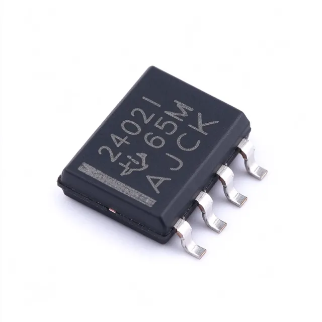
Texas Instruments TLV2402ID is a dual, rail-to-rail input/output operational amplifier designed for low-voltage, low-power signal-conditioning systems. The verified device information identifies a 16 V maximum supply, 5.5 kHz gain-bandwidth product, two amplifier channels, and an 8-pin SOIC package. Its approximately 900 nA per channel supply-current capability makes the TLV2402ID suitable for battery-operated instrumentation where amplifier power must remain small. An operational amplifier is an analog integrated circuit that uses high-gain feedback to amplify the difference between two input voltages. The TLV2402 belongs to the broader operational-amplifier hierarchy, where it combines low quiescent current, rail-to-rail input and output operation, and reverse-battery protection. These characteristics place it between general-purpose precision amplifiers and micropower amplifiers designed for portable or energy-limited equipment. The verified family description identifies rail-to-rail input and output stages, wide supply-voltage capability, high common-mode rejection, and reverse-battery protection. Rail-to-rail input operation allows the input common-mode voltage to extend toward the supply rails, which is important when sensing signals across most of the available input range. Rail-to-rail output operation permits the output to approach either rail, improving usable output swing in low-voltage systems. Reverse-battery protection helps guard the amplifier against excessive current caused by improper battery installation. The 5.5 kHz gain-bandwidth product supports low-frequency signal amplification rather than high-speed waveform processing. Because the dual device provides two amplifiers in one package, both channels use the same supply and are intended to share common operating conditions. The approximately 900 nA per channel supply current is particularly important for battery-powered sensors, portable meters, and industrial monitoring devices that remain active for long periods. Typical applications include low-current sensor conditioning, portable measurement systems, battery-powered monitors, low-frequency filtering, and general-purpose analog signal processing. The 8-pin SOIC package can be assembled using conventional surface-mount production methods, while the dual-channel configuration reduces component count when a design requires two amplified signals or a gain stage plus an active filter. Designers should verify the complete electrical limits, common-mode range, output-swing behavior, stability requirements, and recommended external components in the manufacturer datasheet before releasing a production design. Because the verified information does not include the complete pin table, numeric common-mode-rejection values, input-offset specifications, or recommended external capacitor values, those details require confirmation from the authoritative TLV2402 documentation. This product record combines the verified Texas Instruments family description, distributor availability information, package identification, and design guidance. It also distinguishes the only supported same-footprint substitute found in the supplied cross-reference results and clearly identifies missing technical values that should be obtained from the manufacturer datasheet before precise circuit calculations are performed.

USD $1.43 Dalam Stok
TLV2404CN - 16V Quad Micropower RRIO Op Amp | TI
TLV2404CN

TLV2404CN - 16V Quad Micropower RRIO Op Amp | TI

The Texas Instruments TLV2404CN is a quad micropower operational amplifier with rail-to-rail input and output capability, a 16 V maximum supply designation, 5.5 kHz gain-bandwidth performance, and four amplifiers in a 14-pin PDIP package. It is intended for low-voltage, low-power analog systems that require more than one amplifier on a compact through-hole board. An operational amplifier is a voltage-controlled differential amplifier used to amplify small signals, buffer sensor outputs, perform analog calculations, and drive downstream circuits. The quad TLV2404 belongs to the operational-amplifier hierarchy within analog and mixed-signal semiconductors. Its four channels can reduce external component count and simplify PCB routing compared with four separate single amplifiers, while its micropower positioning supports battery-powered and always-on equipment. Key features include four rail-to-rail input and output amplifiers in one package, a 16 V device rating, and a 5.5 kHz gain-bandwidth product highlighted by Texas Instruments. The rail-to-rail input characteristic supports signal operation across much of the supply range, while rail-to-rail output capability helps preserve output swing near the supply rails. These characteristics are useful in portable sensor interfaces, low-frequency filter stages, and small-signal conditioning circuits. The TLV2404CN is the standard general-purpose TLV2404 configuration identified for a 14-pin PDIP package. According to the manufacturer product page, the family is designed for 2.7 V-class operation as well as higher supply voltages. Its low bandwidth makes it appropriate for energy harvesting, battery monitoring, portable instrumentation, and other applications where high-frequency performance is unnecessary. The through-hole package also supports prototypes, educational platforms, and manually assembled industrial control boards. Typical uses include four-channel sensor conditioning, low-pass and high-pass active filters, transimpedance stages with suitable external biasing, threshold comparators with added hysteresis, and low-frequency signal generators. In each case, resistor and capacitor values determine the practical bandwidth and noise behavior, so simulation and measurement should confirm stability, output swing, and input common-mode limits. For PCB design, route each input and output directly to its corresponding DIP pin, maintain short feedback paths, and place input-sensing traces away from switching nodes. Because the amplifier operates at low bandwidth, bypassing and grounding are often more important than high-speed impedance matching. Check the manufacturer pin-description table before assigning functions to the 14 pins. This product page combines the exact manufacturer and distributor identifiers with practical guidance on package reuse, low-power analog design, and four-channel layout. It also identifies where quotation, lifecycle, and detailed pin verification should be performed before production release.

RFC Hubungi kami
TLV2432CD - Dual 10V 500kHz Rail-to-Rail Op Amp | TI
TLV2432CD

TLV2432CD - Dual 10V 500kHz Rail-to-Rail Op Amp | TI

The Texas Instruments TLV2432CD is a dual, 10 V, 500 kHz CMOS operational amplifier with rail-to-rail output capability, supplied in an 8-pin SOIC package. It combines two amplifier channels, a 10 V maximum supply rating, and a 500 kHz gain-bandwidth product in one compact surface-mount IC. An operational amplifier is an analog building block used to amplify voltage differences, buffer signals, integrate errors, and drive control inputs. The TLV2432 belongs to the CMOS operational-amplifier hierarchy and is designed for low-voltage signal conditioning where two channels, rail-to-rail output swing, and low supply current can simplify a board design. The device is identified as a CMOS, dual-amplifier circuit with rail-to-rail output operation. Its 500 kHz bandwidth is suitable for low-to-moderate-frequency instrumentation, while the 10 V supply rating positions it for circuits operating below the 10 V rail limit. Rail-to-rail output helps the amplifier produce useful output levels near the positive and negative supply rails, although input common-mode limits, output swing, noise, and stability still require verification for each design. The TLV2432CD is offered in an 8-SOIC package and uses two independent amplifier channels. Typical circuit roles include voltage buffering, sensor-signal conditioning, transimpedance conversion, active filtering, and low-frequency closed-loop amplification. Because it is a CMOS operational amplifier, its quiescent behavior is suitable for battery-powered and portable equipment when the operating-current target is compatible with the device specification. Typical applications include industrial sensor interfaces, portable measurement systems, audio signal conditioning, low-frequency control loops, and general-purpose dual-amplifier boards. Two amplifiers per package can reduce component count and PCB area when a design needs matched general-purpose channels. The same package also makes board-level substitutions more practical when the replacement has the same eight-pin pinout and acceptable electrical ratings. For layout, place the decoupling capacitor close to the supply pin, connect exposed-sensitive signals away from power paths, and verify feedback-network stability with the actual load. Do not assume that a rail-to-rail output removes the need for output-headroom checks. Confirm input common-mode range, maximum output current, slew rate, noise, offset, and operating temperature against the manufacturer datasheet before production release. This product page organizes the official device information, exact package identity, sourcing guidance, pin assignment, qualified drop-in alternatives, and practical design notes. It also provides parameter-by-parameter comparisons that help engineers evaluate replacements without confusing a footprint match with guaranteed electrical equivalence.

RFC Hubungi kami
TLV2434ID - 10V 500kHz Quad R-R Op Amp | Texas Instruments
TLV2434ID

TLV2434ID - 10V 500kHz Quad R-R Op Amp | Texas Instruments

Texas Instruments TLV2434ID is a four-channel CMOS operational amplifier designed for low-level signal processing with a 10 V maximum supply, 500 kHz gain-bandwidth product, rail-to-rail output swing, and an extended common-mode input range. The device is packaged in a 14-pin SOIC, allowing four amplifiers to be accommodated on one compact PCB footprint. An operational amplifier is a voltage-controlled, high-gain analog building block used to amplify weak signals, buffer impedance mismatches, compare voltages, perform active filtering, and drive downstream circuitry. Within the power-management and signal-processing hierarchy, the TLV2434ID belongs to the CMOS operational-amplifier family and combines four amplifier channels with low-voltage operation and rail-to-rail output capability. Key features include a 10 V supply rating, 500 kHz gain-bandwidth product, rail-to-rail output operation, and an extended common-mode input range. The rail-to-rail output allows the output voltage to approach the supply rails more closely than a conventional amplifier whose swing is restricted by saturation limits. The four-channel arrangement reduces package count and simplifies PCB routing when a design requires several similar analog functions. The TLV2434ID is a low-voltage CMOS op amp rather than a high-voltage bipolar amplifier. Its rail-to-rail behavior is particularly useful for sensor interfaces, portable instrumentation, battery-powered measurement systems, and signal-conditioning circuits operating from a low-voltage supply. Four independent channels can be used for filtering, buffering, gain stages, or active-feedback sensor conditioning. Typical applications include bridge-based sensor signal conditioning, low-level audio and communication interfaces, current monitoring, analog measurement front ends, active filters, and multi-channel test equipment. When designing around the device, confirm that input and output voltages remain within the common-mode and output-swing limits for the selected supply. Decoupling capacitors should be placed close to the supply pins, while sensitive inputs require short traces and a low-noise ground return. This product page combines the manufacturer’s device description, package information, cross-reference findings, application guidance, and engineering-focused selection criteria to support faster sourcing and board-level planning for the TLV2434ID.

RFC Hubungi kami
TLV2442ID - Dual Rail-to-Rail Output Op Amp | Texas Instruments
TLV2442ID

TLV2442ID - Dual Rail-to-Rail Output Op Amp | Texas Instruments

Texas Instruments TLV2442ID is a dual Advanced LinCMOS operational amplifier with rail-to-rail output capability and wide-input-voltage operation. The device contains two amplifier circuits, operates from 2.7 V to 10 V, and is available in an 8-pin SOIC package. Its 1.75 MHz gain-bandwidth product and 1.3 V/µs slew rate make it suitable for low-power signal-conditioning designs that require more bandwidth than a basic micropower amplifier. An operational amplifier is a voltage-feedback amplifier used to amplify, buffer, filter, or compare small analog signals. The TLV2442 belongs to the CMOS operational-amplifier hierarchy within the broader amplifier IC and semiconductor categories. Unlike a rail-to-rail input device, the TLV2442 is specifically described by Texas Instruments as having a rail-to-rail output and wide-input-voltage range. This distinction matters when the output must approach the supply rails but the input does not need to cover both rails fully. Key characteristics include two amplifier circuits in one package, a 2.7 V to 10 V supply range, 1.75 MHz bandwidth, and a 1.3 V/µs slew rate. The rail-to-rail output is particularly useful for driving downstream circuits that operate near a supply rail. Combining two amplifiers in one SOIC-8 package can also reduce board area and simplify dual-channel signal paths such as sensor conditioning, filtering, or differential analog front ends. The Advanced LinCMOS implementation supports low-voltage operation while preserving useful dynamic performance for portable and embedded equipment. Bandwidth determines how quickly the closed-loop amplifier can process small-signal variations, while slew rate describes the maximum rate at which the output can change in a large-signal step. These characteristics make the TLV2442 appropriate for audio, instrumentation, communication, and control applications where the signal bandwidth remains below the amplifier’s 1.75 MHz capability. Typical uses include low-frequency sensor amplification, active filtering, audio signal conditioning, general-purpose buffering, and dual-channel analog processing. Battery-operated products benefit from the 2.7 V minimum supply voltage because the amplifier can operate directly from a single 3.3 V rail. The same SOIC-8 package is convenient for prototypes and production assemblies requiring a conventional surface-mount footprint. Designers should verify the input common-mode range, output swing, noise, offset, stability, and output-current capability against the manufacturer datasheet for the intended supply and load conditions. Decoupling capacitors should be placed close to the supply pins, and unused amplifier inputs must be configured according to the recommended circuit practice. Proper grounding and short feedback paths are essential for predictable settling and reduced channel interaction. This page combines the manufacturer’s device description with package, electrical, sourcing, replacement, and application guidance. It also identifies the limits of the available cross-reference information so that engineers can distinguish a verified drop-in option from variants that require a different footprint or a new design qualification.

RFC Hubungi kami
TLV2442QD - Dual RRO CMOS Op Amp | Texas Instruments
TLV2442QD

TLV2442QD - Dual RRO CMOS Op Amp | Texas Instruments

Texas Instruments TLV2442QD is a dual CMOS operational amplifier featuring rail-to-rail output operation and a wide-input-voltage architecture in an 8-pin SOIC package. It combines two amplifier channels in one package, operates from a single 5 V supply in the documented application, and supports input signals approaching the supply rails. The device is listed by Texas Instruments as an Advanced LinCMOS rail-to-rail-output wide-input-voltage operational amplifier, making it suitable for general-purpose signal conditioning, instrumentation, and analog control circuits. An operational amplifier is an analog building block that amplifies the voltage difference between its inverting and non-inverting inputs. The TLV2442 family uses CMOS circuitry to provide rail-to-rail output behavior, while its extended common-mode input range allows the inputs to operate closer to the supply rails than a conventional CMOS amplifier. Two independent channels in one SOIC package can reduce board area and simplify dual-axis, filtering, buffering, or complementary signal-processing designs. The manufacturer identifies low noise and no phase inversion as important characteristics of this family. The reported gain-bandwidth value is 1.81 MHz, which makes the amplifier suitable for moderate-bandwidth instrumentation and control paths. Its 4.25 V minimum supply requirement at a 5 V single-supply operating point is another defining feature. Because the output can swing toward both supply rails, signal-chain designers gain additional usable output range without requiring a separate output-bias arrangement. The TLV2442 architecture is intended for low-voltage, low-power analog systems where two amplifier channels are needed in a compact package. Rail-to-rail output improves dynamic range in sensor interfaces and single-supply signal chains, while the wide common-mode input range accommodates input voltages near the rails. These characteristics make the device appropriate where conventional restricted-output amplifiers would clip or lose signal margin at low or high signal levels. Typical uses include sensor-signal conditioning, low-side current measurement, portable instrumentation, industrial control modules, audio input buffers, and general dual-channel filtering. In a two-axis sensing system, both channels can amplify signals with the same supply and package. In a filter or driver arrangement, the second channel may condition a complementary signal or support feedback around an external active network. Designers should verify input and output limits, common-mode behavior, output-current capability, noise, and stability for the intended operating point before finalizing the circuit. Decoupling capacitors should be placed close to the supply pins, and sensitive analog layouts should minimize trace resistance and coupling from switching circuitry. The Q suffix identifies the automotive-related ordering variant, so qualification and temperature requirements should be checked against the final operating environment. This page consolidates the device identity, operating characteristics, drop-in-family alternatives, package information, and practical implementation guidance for engineers evaluating the TLV2442QD. It also distinguishes same-footprint family options from broader functional equivalents so board-level replacement decisions begin with the required package and qualification constraints.

RFC Hubungi kami
TLV2444CD - Quad Rail-to-Rail CMOS Op Amp | Texas Instruments
TLV2444CD

TLV2444CD - Quad Rail-to-Rail CMOS Op Amp | Texas Instruments

Texas Instruments TLV2444CD is a quad, rail-to-rail-output, wide-input-voltage CMOS operational amplifier packaged in a 14-pin SOIC. The device contains four amplifier circuits, provides output swing that includes both supply rails, and uses an extended common-mode input voltage range. According to the manufacturer product information, it operates from single or dual supplies and supports rail-to-rail output operation for low-voltage analog signal-conditioning systems. An operational amplifier is a voltage-gain amplifier used to amplify, buffer, filter, compare, or reshape analog signals. The TLV2444 belongs to the linear-amplifier hierarchy, combining low-voltage CMOS operation with rail-to-rail output capability. Its wide input-voltage range makes it useful when signals approach the available supply voltage, while the four amplifiers in one package can support several signal paths in compact equipment. Key features include four amplifier circuits, rail-to-rail output swing, an extended common-mode input range, low-noise operation, and no output phase inversion. A single-supply configuration requires at least 4.25 V. The CMOS design is intended for portable instrumentation, industrial control, data acquisition, and portable equipment where low-voltage analog signals must be conditioned without relying on a dual supply. The LinCMOS architecture positions the TLV2444 between conventional CMOS and bipolar operational amplifiers. Rail-to-rail output allows the output voltage to approach the positive and negative supply limits under suitable load conditions. The extended common-mode range is particularly valuable in battery-powered designs because sensor outputs can occupy much of the available signal range. Four amplifiers in one 14-pin SOIC also reduce board area compared with separate single or dual amplifier packages. Typical applications include sensor signal conditioning, portable measurement equipment, battery-powered data acquisition, industrial interface circuits, low-voltage comparators, and active filtering. Each amplifier can be configured for inverting, non-inverting, voltage-follower, or feedback-based filtering operation, provided the designer observes the input, output, and common-mode limits from the manufacturer data sheet. Design attention should focus on input bias current, output load capability, noise, bandwidth, stability with capacitive loads, and the selected feedback network. Because the exact electrical limits are product-specific, use the pin-description table and characteristic curves in the manufacturer data sheet when assigning input and output pins or sizing external resistors and capacitors. This product page organizes the TLV2444CD family information, exact package attributes, technical specifications, sourcing workflow, and engineering considerations for faster design review. It also distinguishes the available manufacturer alternatives from cross-brand parts and highlights where PCB-level verification remains essential before substituting any amplifier.

RFC Hubungi kami
TLV2444ID - Quad Rail-to-Rail CMOS Op Amp | Texas Instruments
TLV2444ID

TLV2444ID - Quad Rail-to-Rail CMOS Op Amp | Texas Instruments

The Texas Instruments TLV2444ID is a four-circuit, Advanced LinCMOS operational amplifier with rail-to-rail output swing, wide-input-voltage capability, and low-voltage operation in a 14-pin SOIC package. The device is designed for single- or dual-supply systems where low power, compact implementation, and flexible input ranges are important. Its operating temperature range extends from -40°C to 125°C, making it suitable for industrial, instrumentation, communications, and embedded control applications. An operational amplifier is an analog signal-processing IC that amplifies the voltage difference between its differential inputs. The operational-amplifier category includes voltage-feedback and current-feedback devices, while the TLV2444ID is a voltage-feedback, CMOS quad amplifier. Four amplifiers in one package reduce board area and simplify designs requiring multiple low-voltage signal stages, buffers, or gain channels. Key features of the TLV2444ID include rail-to-rail output operation, a wide common-mode input voltage range, CMOS construction, and four amplifiers per package. Rail-to-rail output swing allows the output voltage to approach the supply rails, maximizing usable signal range in low-voltage systems. The wide input range is particularly useful when sensor outputs, divided signals, or bias voltages occupy much of the available supply voltage. The Advanced LinCMOS architecture supports low-voltage operation while maintaining low bias current and low-noise behavior. Because the amplifiers do not phase invert, they can be used in conventional inverting and non-inverting signal paths. A single package can implement filters, instrumentation amplifiers, sensor amplifiers, level-shifting stages, or analog signal-conditioning blocks while preserving consistent device characteristics across all four channels. Typical applications include portable instrumentation, battery-powered sensor interfaces, industrial control systems, audio and communication signal conditioning, data-acquisition front ends, and low-voltage analog processing. The 14-pin SOIC package supports conventional surface-mount assembly and provides a practical upgrade from discrete single or dual amplifier implementations when four independent channels are required. When designing around the TLV2444ID, verify the input common-mode range, output swing, supply current, stability requirements, and input-capacitance limits against the intended operating conditions. Decoupling capacitors should be placed close to the supply pins, and sensitive analog traces should be kept away from switching nodes and high-current return paths. This product page combines the manufacturer product information with practical guidance for package selection, pinout use, application fitting, design trade-offs, and verified drop-in alternatives. It is intended to help engineers determine whether the TLV2444ID's four-channel CMOS architecture and 14-pin SOIC footprint align with a new analog-front-end design or an existing board revision.

RFC Hubungi kami