5M1270ZT144A5N vs 5M1270ZT144C5N Pengandingan
Pengandingan Sisi Kiri Sisi Kanan Terperinci 5M1270ZT144A5N disebabkan oleh Intel dan 5M1270ZT144C5N disebabkan oleh Altera. Bandingkan spesifikasi utama, parameter elektrik, pakej, status kehidupan, harga, dan keupayaan untuk menentukan komponen terbaik untuk keperluan disenjaya anda.
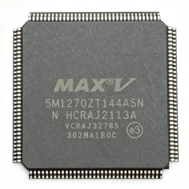
Altera

5M1270ZT144C5N - MAX V CPLD 980 Macrocells 114 I/O TQFP-144 | Intel / Altera
5M1270ZT144C5N ✓ AktifPengandingan Spesifikasi
| Parametr | 5M1270ZT144A5N | 5M1270ZT144C5N |
|---|---|---|
| Merek | Intel | Altera |
| Kategori | FPGA & CPLD | FPGA & CPLD |
| Status Lingkungan Hidup | Aktif | Aktif |
| Harga Unit (USD) | $19.85 | — |
| Family | MAX V | — |
| Device Type | CPLD (Complex Programmable Logic Device) | CPLD (Complex Programmable Logic Device) |
| Macro Cells | 980 | — |
| User I/Os | 114 | 114 |
| Logic Elements | 2120 (approx.) | 1270 |
| User Flash Memory | 8 Kbits | — |
| Maximum Operating Frequency | 201.1 MHz | — |
| Speed Grade | 5N | — |
| Core Supply Voltage | 1.8 V | — |
| I/O Bank Voltage Support | 1.8 V / 2.5 V / 3.3 V / 5.0 V (MultiVolt) | — |
| Kemasan | TQFP-144 (T144) | TQFP-144 (22 x 22 mm, 0.5 mm pitch) |
| Jenis Pemasangan | Surface Mount | Surface Mount |
| Process Technology | Non-volatile flash CMOS | — |
| Programming Interface | JTAG (IEEE 1149.1) | JTAG in-system programmable (Altera Quartus II) |
| Design Software | Quartus II / Quartus Prime | — |
| Suhu Operasi | -40C to +125C (automotive) | 0 C to +85 C (commercial grade) |
| Automotive Qualification | AEC-Q100 | — |
| Status RoHS | Compliant | Compliant |
| Internal Features | Pull-up resistors, bus-hold, on-chip oscillator | — |
| Series | — | MAX V |
| Macrocells | — | 980 |
| Maximum Internal Frequency | — | 118.3 MHz |
| Pin-to-Pin Propagation Delay (tPD) | — | 6.2 ns |
| Internal Frequency (typical) | — | 201 MHz |
| User Flash Memory (UFM) | — | 8 Kbits |
| Configuration Memory | — | Flash (non-volatile, in-system programmable) |
| VCCINT (Core Supply) | — | 1.71 V to 1.89 V |
| VCCIO (I/O Supply, per bank) | — | 1.2 V to 3.3 V |
| Number of I/O Banks | — | 4 |
| Supported I/O Standards | — | LVCMOS, LVTTL, PCI up to 3.3 V, 1.2 V to 3.3 V LVCMOS on JTAG pins |
| JTAG Interface | — | IEEE 1149.1 (TMS, TDI, TDO, TCK in Bank 1) |
| Program/Erase Cycles | — | Up to 100,000 |