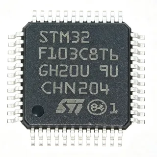
STM32F103C8T6TR - 72MHz Cortex-M3 MCU, 64KB Flash, LQFP-48 | STMicroelectronics (Tape & Reel)
MPN: STM32F103C8T6TR ✓ AktifSTM32F103C8T6TR Ringkasan
An ARM Cortex-M3 microcontroller (MCU) is a 32-bit RISC processor core designed by Arm Holdings for embedded applications requiring deterministic real-time performance at low power. The Cortex-M3 sits at the lower end of the Cortex-M family (above Cortex-M0/M0+ and below Cortex-M4/M7), and microcontrollers in this category combine the processor core with on-chip memory, peripherals, and analog blocks into a single system-on-chip. The STM32F103 family specifically belongs to the broader hierarchy: ARM Cortex-M3 -> 32-bit MCU -> STM32F1 series -> STM32 mainstream family -> STMicroelectronics microcontrollers -> semiconductor. This hierarchy matters because it determines the toolchain (Arm Cortex-M3 supports the standard Arm Keil, IAR, GCC, and STM32CubeIDE flows) and the peripheral programming model used across the STM32 platform.
Key features include 64 KB of embedded Flash with read-while-write capability, 20 KB of SRAM, a 2.0 V to 3.6 V supply range, an 8 MHz internal RC oscillator with PLL multiplier to 72 MHz, two 12-bit ADCs (1 µs conversion, up to 16 channels), seven 16-bit timers, and a full-speed USB 2.0 Full-Speed device/host/OTG controller. Communication peripherals include three USARTs, two SPIs (18 Mbit/s), two I2C buses (400 kHz), one CAN 2.0B interface, and one USB Full-Speed port. The 48-pin LQFP package exposes 37 GPIO pins tolerant to 5 V.
Architecturally, the Cortex-M3 core delivers 1.25 Dhrystone MIPS per MHz, supports the Thumb-2 instruction set, and includes a Nested Vectored Interrupt Controller (NVIC) with configurable priority and hardware stack handling. The integrated voltage regulator and brown-out reset (BOR) simplify power design, while the 4-byte backup register with a tamper-detection pin supports battery-backed RTC modes.
Typical applications include industrial control boards, motor drives (BLDC/PMSM FOC complements), USB HID/COM port devices, CAN-bus node interfaces, and low-cost development platforms such as the well-known "Blue Pill" board.
When designing with this device, place a 100 nF ceramic decoupling capacitor as close as possible to each VDD/VDDA pin pair, and reserve the NRST pin connection for a 10 kΩ pull-up and optional reset button. Ensure the BOOT0 pin state matches the desired boot memory on every power-up.
This page synthesizes distributor pricing, drop-in alternatives (same-brand STM32F103 variants first, then cross-brand pin-compatible parts), and practical design notes not found in the manufacturer datasheet.
Pilihan pengganti yang segera untuk STM32F103C8T6TR — sama paket, pin-pin kompatibel. Bahagian paket yang berbeza memerlukan kerja ulang PCB diasingkan.
Varietas dalam siri ini
Model serupa yang kompatibel dengan pengganti yang segera STM32F103C8T6TR (sama faktor bentuk dan kaki) — berbeza dalam ADC, CAN, Flash Memory, Operating Temperature, Package.
STM32F103C8T7
Hubungi untuk harga
Lihat Datasheet →GD32F103C8T6
📋 Alternatif rujukan (tidak dalam katalog)
APM32F103C8T6
📋 Alternatif rujukan (tidak dalam katalog)
STM32F103C8T6TR Penilaian maksimum & Ciri-ciri Elektrik
| Core Architecture | ARM Cortex-M3 (32-bit RISC) |
| Frekuensi Klock Maksimum | 72 MHz |
| Flash Memory | 64 KB |
| SRAM | 20 KB |
| Supply Voltage (VDD) | 2.0 V to 3.6 V |
| Kemasan | LQFP-48 (7x7 mm, 0.5 mm pitch) |
| GPIO Count | 37 |
| ADC | 2x 12-bit, 1 µs, up to 16 channels |
| Timers | 7x 16-bit (including 1x watchdog, 2x SysTick) |
| USART | 3 |
| SPI | 2 (18 Mbit/s) |
| I2C | 2 (400 kHz) |
| USB | 1x USB 2.0 Full-Speed device/host/OTG |
| CAN | 1x CAN 2.0B |
| Suhu Operasi | -40 °C to +85 °C (industrial grade) |
| Status RoHS | Compliant |
Konfigurasi Pin STM32F103C8T6TR
| Pin 1 | VBAT — Backup battery supply input |
| Pin 2 | PC13 — GPIO PC13, anti-tamper (RTC) |
| Pin 3 | PC14 — GPIO PC14 / OSC32_IN |
| Pin 4 | PC15 — GPIO PC15 / OSC32_OUT |
| Pin 5 | OSC_IN — HSE oscillator input |
| Pin 6 | OSC_OUT — HSE oscillator output |
| Pin 7 | NRST — Reset input, active-low |
| Pin 8 | VSSA — Analog ground |
| Pin 9 | VDDA — Analog supply (2.4 V - 3.6 V) |
| Pin 10 | PA0 — GPIO PA0 / WKUP / ADC_IN0 / TIM2_CH1 |
| Pin 11 | PA1 — GPIO PA1 / ADC_IN1 / TIM2_CH2 |
| Pin 12 | PA2 — GPIO PA2 / USART2_TX / ADC_IN2 |
| Pin 13 | PA3 — GPIO PA3 / USART2_RX / ADC_IN3 |
| Pin 14 | PA4 — GPIO PA4 / SPI1_NSS / ADC_IN4 |
| Pin 15 | PA5 — GPIO PA5 / SPI1_SCK / ADC_IN5 |
| Pin 16 | PA6 — GPIO PA6 / SPI1_MISO / ADC_IN6 |
| Pin 17 | PA7 — GPIO PA7 / SPI1_MOSI / ADC_IN7 |
| Pin 18 | PB0 — GPIO PB0 / ADC_IN8 / TIM3_CH3 |
| Pin 19 | PB1 — GPIO PB1 / ADC_IN9 / TIM3_CH4 |
| Pin 20 | PB2 — GPIO PB2 / BOOT1 (also PB-BOOT input) |
| Pin 21 | PB10 — GPIO PB10 / I2C2_SCL / USART3_TX |
| Pin 22 | PB11 — GPIO PB11 / I2C2_SDA / USART3_RX |
| Pin 23 | VSS_1 — Digital ground |
| Pin 24 | VDD_1 — Digital supply (2.0 V - 3.6 V) |
| Pin 25 | PB12 — GPIO PB12 / SPI2_NSS / CAN2_RX |
| Pin 26 | PB13 — GPIO PB13 / SPI2_SCK / CAN2_TX / USB_DP pull-up |
| Pin 27 | PB14 — GPIO PB14 / SPI2_MISO |
| Pin 28 | PB15 — GPIO PB15 / SPI2_MOSI |
| Pin 29 | PA8 — GPIO PA8 / USART1_CK / TIM1_CH1 |
| Pin 30 | PA9 — GPIO PA9 / USART1_TX / TIM1_CH2 |
| Pin 31 | PA10 — GPIO PA10 / USART1_RX / TIM1_CH3 |
| Pin 32 | PA11 — GPIO PA11 / CAN1_RX / USBDM (USB data minus) |
| Pin 33 | PA12 — GPIO PA12 / CAN1_TX / USBDP (USB data plus) |
| Pin 34 | PA13 — GPIO PA13 / JTMS / SWDIO |
| Pin 35 | VSS_2 — Digital ground |
| Pin 36 | VDD_2 — Digital supply (2.0 V - 3.6 V) |
| Pin 37 | PA14 — GPIO PA14 / JTCK / SWCLK |
| Pin 38 | PA15 — GPIO PA15 / JTDI |
| Pin 39 | PB3 — GPIO PB3 / JTDO / TRACESWO |
| Pin 40 | PB4 — GPIO PB4 / JNTRST |
| Pin 41 | PB5 — GPIO PB5 / I2C1_SMBAI |
| Pin 42 | PB6 — GPIO PB6 / I2C1_SCL / TIM4_CH1 |
| Pin 43 | PB7 — GPIO PB7 / I2C1_SDA / TIM4_CH2 |
| Pin 44 | BOOT0 — Boot mode select (0 = Flash, 1 = System bootloader) |
| Pin 45 | PB8 — GPIO PB8 / TIM4_CH3 |
| Pin 46 | PB9 — GPIO PB9 / TIM4_CH4 |
| Pin 47 | VSS_3 — Digital ground |
| Pin 48 | VDD_3 — Digital supply (2.0 V - 3.6 V) |
Aplikasi Biasa
STM32F103C8T6TR patut untuk 6 aplikasis: Industrial Control Boards, USB HID / Virtual COM Port Devices, BLDC / PMSM Motor Drives, CAN-Bus Node Interface, Low-Cost Development Platforms ("Blue Pill"), IoT Sensor / Smart Home Edge Nodes.
Industrial Control Boards
The STM32F103C8T6TR fits industrial control boards because its 72 MHz Cortex-M3 core and 64 KB Flash comfortably handle Modbus RTU slave firmware, PID loop control, and user-interface logic on a single chip. The dual 12-bit ADCs (1 µs, up to 16 channels) sample 4-20 mA sensor inputs at the kHz rates typical of PLC analog modules, while the three USARTs (USART1/2/3) support simultaneous RS-232/RS-485 fieldbus and a debug console. The 2.0 V to 3.6 V supply range aligns with 3.3 V industrial backplanes, and the -40 °C to +85 °C operating temperature meets most cabinet-mounted equipment specs. On-board CAN 2.0B lets a single MCU handle both a sensor bus and an external CANopen master.
Disebarkan
USB HID / Virtual COM Port Devices
The STM32F103C8T6TR's integrated USB 2.0 Full-Speed device controller (12 Mbit/s) makes it a natural fit for USB HID-class peripherals, virtual COM-port bridges, and CDC-MSC composite devices without external PHY hardware. The 72 MHz core and 20 KB SRAM execute the standard ST USB device library (and STM32CubeMX-generated middleware) with room left for application logic, while the 64 KB Flash fits typical HID report descriptors and command parsers. Its 2.0 V to 3.6 V rail tolerance lets designers tap the USB 5 V bus through an LDO and run the MCU from a single 3.3 V supply. Designers should add ESD protection (USBLC6-2SC6) and a 1.5 kΩ pull-up on the D+ line to the USB connector.
Disebarkan
BLDC / PMSM Motor Drives
The STM32F103C8T6TR is widely used in sensorless or hall-sensored BLDC and PMSM motor drives for low- to mid-power applications (fans, pumps, e-bike hubs). Its 72 MHz Cortex-M3 plus advanced timers (TIM1 with complementary PWM and dead-time insertion) generate the 6-step or space-vector PWM that drives a 3-phase inverter at up to tens of kHz switching. The two ADCs trigger from timer events to sample phase currents within the PWM cycle for low-latency commutation, and the quadrature encoder interface on TIM2 supports sensored FOC firmware patterns. CAN bus readiness lets the drive communicate with a central PLC, while the 2.0-3.6 V range accepts a wide range of bus-powered motor-control supplies.
Disebarkan
CAN-Bus Node Interface
The STM32F103C8T6TR is a battle-tested choice for CAN 2.0B node interfaces used in automotive body-electronics, industrial CANopen, and medical device buses. The bxCAN peripheral supports standard and extended frames with hardware filter banks and a 1 Mbit/s bit rate suitable for most fieldbus deployments. With 64 KB Flash the device holds small CANopen/CANFestival stacks and application logic, while three USARTs allow a companion GPS or HMI link. Operating temperature of -40 °C to +85 °C suits non-automotive nodes; designers needing AEC-Q100 should select the STM32F103C8T7 variant. Drop a 60 Ω termination resistor only on the bus ends and add a TJA1050 or TCAN332 transceiver externally.
Disebarkan
Low-Cost Development Platforms ("Blue Pill")
The STM32F103C8T6TR is the headline MCU of the iconic "Blue Pill" development board that became the de-facto entry ticket to ARM Cortex-M3 firmware development. Its 72 MHz core, 64 KB Flash, SWD debug pins, USB connector, and 48-pin LQFP form factor fit on a 53 x 23 mm PCB with a USB micro-B port, a 3.3 V LDO, a reset button, and boot-mode jumpers. Students and hobbyists target it with STM32CubeIDE, PlatformIO, and the Arduino STM32 core, and any prototype firmware written on the Blue Pill ports directly to custom hardware when the same MCU is kept on the production board. The LQFP-48 footprint is also shared by several GD32 and APM32 pin-compatibles, simplifying second sourcing for educational kits.
Disebarkan
IoT Sensor / Smart Home Edge Nodes
The STM32F103C8T6TR handles Smart Home and IoT edge nodes that need local sensor aggregation, BLE/Wi-Fi module handshaking, and OTA bootloading without committing to a high-cost M4-class part. Three USARTs (USART1/2/3) drive an ESP-01 Wi-Fi co-processor, a GPS module, and a debug console in parallel; two SPIs (up to 18 Mbit/s) talk to a LoRa SX1278 or a small TFT display; two I2C buses serve a BME280 environmental sensor and an OLED panel. The 12-bit ADC samples analog sensors such as soil-moisture probes, and the RTC plus 4-byte backup register keep a wall-clock time across deep-sleep cycles powered by a CR2032. The 2.0-3.6 V supply range supports direct lithium-ion battery operation via an LDO or buck.
Disebarkan
Ringkasan Produk Disebarkan
Data referensi kejuruteraan untuk STM32F103C8T6TR — perbandingan, panduan rancangan, dan maklumat kesediaan
Panduan Pilihan
Perbandingan dengan Gantian
| Parametr | Produk Ini | STM32F103CBT6 | STM32F103C8T7 | GD32F103C8T6 | APM32F103C8T6 | STM32F030C8T6 |
|---|---|---|---|---|---|---|
| Brand | STMicroelectronics | STMicroelectronics | STMicroelectronics | GigaDevice | GigaDevice | STMicroelectronics |
| Package | LQFP-48 (7x7 mm) | LQFP-48 (7x7 mm) - same | LQFP-48 (7x7 mm) - same | LQFP-48 (7x7 mm) - same | LQFP-48 (7x7 mm) - same | LQFP-48 (7x7 mm) - same |
| Core | ARM Cortex-M3 | ARM Cortex-M3 | ARM Cortex-M3 | ARM Cortex-M3 | ARM Cortex-M3 | ARM Cortex-M0 (-1 class) |
| Max Clock | 72 MHz | 72 MHz | 72 MHz | 108 MHz (+50%) | 96 MHz (+33%) | 48 MHz (-33%) |
| Flash | 64 KB | 128 KB (+100%) | 64 KB | 64 KB | 64 KB | 64 KB |
| SRAM | 20 KB | 20 KB | 20 KB | 20 KB | 20 KB | 8 KB (-60%) |
| USB | USB 2.0 Full-Speed | USB 2.0 Full-Speed | USB 2.0 Full-Speed | USB 2.0 Full-Speed | USB 2.0 Full-Speed | No USB |
| CAN | 1x CAN 2.0B | 1x CAN 2.0B | 1x CAN 2.0B | 1x CAN 2.0B | 1x CAN 2.0B | No CAN |
| Automotive Grade | No (industrial -40/+85C) | No | Yes (AEC-Q100) | No | No | No |
Penyeberangsung Jelas
- Pin-compatible Flash-doubled drop-in within the same family (vsSTM32F103CBT6)
- AEC-Q100 automotive temperature grade available on the same silicon/die (vsSTM32F103C8T7)
- Two- to four-times faster core on the same LQFP-48 footprint (vsGD32F103C8T6)
Catatan Desain
Place 100 nF ceramic decoupling capacitors as close as possible to every VDD/VDDA pin pair (pins 24, 36, 48 / 9), with at least one bulk 4.7 µF capacitor on the main 3.3 V rail within 20 mm. VDDA requires a low-impedance connection; if the main 3.3 V supply is noisy, insert a ferrite bead between VDD and VDDA. Tie VBAT to VDD if a backup battery is not used. Always keep the BOOT0 pin held low at power-up to default-boot from Flash.
Route the 8 MHz HSE crystal traces short and symmetric, with the crystal placed within 5 mm of OSC_IN/OSC_OUT (pins 5/6) and the load capacitors (typically 20-30 pF) grounded right at the crystal case. Keep USB D+/D- (PA11/PA12) matched-length (target <2 mm delta) and place the 1.5 kΩ pull-up on D+ next to the connector, not the MCU side. Provide a 10 kΩ pull-up on NRST and a low-impedance path to GND through a reset push-button.
When using CAN or USB, add a TVS diode array such as USBLC6-2SC6 or PESD1CAN close to the connector to meet IEC 61000-4-2 ±8 kV air-discharge and ±4 kV contact-discharge ratings. The internal pull-up on USB D+ (PA12) is not strong enough for reliable enumeration; an external 1.5 kΩ resistor to 3.3 V is recommended. CAN bus termination should use 120 Ω at both ends only, with a split-capacitor network for stub suppression in multi-node harnesses.
Do not leave BOOT0 floating - noise on this pin during power-up will intermittently boot the MCU into the system bootloader and the application code will appear to be missing. Three common mistakes: (1) leaving VBAT floating instead of tying it to VDD, which charges the internal diode and corrupts backup register writes; (2) using PA13/PA14 as GPIO without disabling JTAG/SWD, since JTAG defaults to these pins after reset; (3) configuring GPIO output speed to '50 MHz' on I2C pins, which causes ringing - always select '2 MHz' open-drain with external pull-ups.
Maklumat Kesediaan
RoHS-compliant per ST product page; AEC-Q100 grade is a separate SKU (STM32F103C8T7). Halogen-free status not explicitly verified in the provided data and flagged as 'unknown'.