STM32F103CBT6 - 72MHz Cortex-M3, 128KB Flash MCU | ST
MPN: STM32F103CBT6 ✓ Active| Qty | Unit Price | Extended |
|---|---|---|
| 1 | $4.2 | $4.20 |
| 10 | $3.78 | $37.80 |
| 100 | $3.15 | $315.00 |
| 500 | $2.75 | $1,375.00 |
| 1,000 | $2.4 | $2,400.00 |
STM32F103CBT6 Overview
What is a microcontroller? An MCU integrates a processor core, on-chip memory (Flash and SRAM), and programmable peripherals on a single die, sitting above a bare microprocessor and below a full system-on-chip in the embedded hierarchy. The STM32F1 mainstream series positions the STM32F103CBT6 as a workhorse general-purpose controller between the low-power STM32L series and the higher-performance STM32F4 series.
Key features include a 72 MHz Cortex-M3 core with single-cycle multiply and hardware divide, a 2.0V to 3.6V supply range, up to 37 GPIOs, two 12-bit ADCs with up to 10 external channels, three general-purpose 16-bit timers, one advanced-control PWM timer, and one basic timer. Communication coverage is unusually complete for this class: three USARTs, two I2C, two SPI, a full-speed USB 2.0 device interface, and a CAN 2.0B active controller.
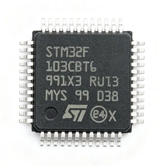
Technically, the device offers a nested vectored interrupt controller with 43 maskable channels, flexible clocking from an internal 8 MHz RC oscillator, a 4-16 MHz external crystal, or a 32 kHz RTC oscillator, plus PLL multiplication to 72 MHz. The LQFP-48 package provides a compact 7x7 mm footprint suited to dense industrial boards.
Typical applications include industrial control nodes, motor drives, USB and CAN fieldbus devices, medical instruments, and IoT gateways, where the combination of CAN, USB, and multiple UARTs makes the part a natural communication hub.
For design, decouple every VDD pin with 100 nF ceramics plus one bulk capacitor, and configure BOOT0 correctly for the desired boot source (Flash, system memory, or SRAM). Firmware is flashed and debugged in-circuit via SWD or JTAG.
This page synthesizes distributor pricing, pin-compatible drop-in alternatives such as GD32F103CBT6 and APM32F103CBT6, and practical design notes not found in the ST datasheet.
Drop-in alternatives for STM32F103CBT6 — same package, pin-to-pin compatible. Different-package parts requiring PCB rework are excluded.
Variants in this series
Same-series models that are drop-in compatible with STM32F103CBT6 (same form factor and footprint) — differing in Core, Flash Memory, Package, SRAM, ADC Resolution.
Quick Comparison Tool — Select alternative parts for side-by-side comparison:
STM32F103C8T6
✅ Drop-In✓ In Stock
$1.02 / Unit
View Datasheet →STM32F302CBT6
✅ Drop-In✓ In Stock
$3.1 / Unit
View Datasheet →GD32F103CBT6
✅ Drop-In📋 Reference alternative (not in catalog)
APM32F103CBT6
✅ Drop-In📋 Reference alternative (not in catalog)
AT32F403ACGT7
✅ Drop-In📋 Reference alternative (not in catalog)
CH32F103C8T6
✅ Drop-In📋 Reference alternative (not in catalog)
STM32F103CBT6 Maximum Ratings & Electrical Characteristics
| Core | ARM Cortex-M3 |
| Core Size | 32-bit |
| Maximum Clock Frequency | 72 MHz |
| Flash Memory | 128 KB (128K x 8) |
| SRAM | 20 KB |
| Supply Voltage Range | 2.0 V to 3.6 V |
| GPIO Count | 37 |
| ADC Resolution | 12-bit x 2 (up to 10 external channels) |
| USART | 3 |
| I2C | 2 |
| SPI | 2 |
| USB | USB 2.0 full-speed device |
| CAN | CAN 2.0B active |
| Timers | 3 general-purpose, 1 advanced-control, 1 basic (16-bit) |
| Interrupt Channels (NVIC) | 43 maskable |
| Package | LQFP-48 (7x7 mm) |
| Mounting Type | Surface Mount |
| Debug Interfaces | SWD, JTAG |
STM32F103CBT6 Pin Configuration
| Pin 1 | VBAT — Battery backup supply for RTC and backup registers |
| Pin 2 | PC13 — GPIO port C, pin 13 (TAMPER-RTC) |
| Pin 3 | PC14 — GPIO port C, pin 14 / OSC32_IN |
| Pin 4 | PC15 — GPIO port C, pin 15 / OSC32_OUT |
| Pin 5 | PD0/OSC_IN — GPIO port D pin 0 / main crystal input |
| Pin 6 | PD1/OSC_OUT — GPIO port D pin 1 / main crystal output |
| Pin 7 | NRST — System reset (active low) |
| Pin 8 | VSSA — Analog ground |
| Pin 9 | VDDA — Analog power supply (2.0-3.6 V) |
| Pin 10 | PA0 — GPIO / ADC12_IN0 / WKUP / TIM2_CH1 |
| Pin 11 | PA1 — GPIO / ADC12_IN1 / TIM2_CH2 |
| Pin 12 | PA2 — GPIO / ADC12_IN2 / USART2_TX / TIM2_CH3 |
| Pin 13 | PA3 — GPIO / ADC12_IN3 / USART2_RX / TIM2_CH4 |
| Pin 14 | PA4 — GPIO / ADC12_IN4 / SPI1_NSS / DAC_OUT1 |
| Pin 15 | PA5 — GPIO / ADC12_IN5 / SPI1_SCK / DAC_OUT2 |
| Pin 16 | PA6 — GPIO / ADC12_IN6 / SPI1_MISO / TIM3_CH1 |
| Pin 17 | PA7 — GPIO / ADC12_IN7 / SPI1_MOSI / TIM3_CH2 |
| Pin 18 | PC4 — GPIO / ADC12_IN14 |
| Pin 19 | PC5 — GPIO / ADC12_IN15 |
| Pin 20 | PB0 — GPIO / ADC12_IN8 / TIM3_CH3 |
| Pin 21 | PB1 — GPIO / ADC12_IN9 / TIM3_CH4 |
| Pin 22 | PB2/BOOT1 — GPIO / boot pin 1 |
| Pin 23 | PB10 — GPIO / I2C2_SCL / USART3_TX / TIM2_CH3 remap |
| Pin 24 | PB11 — GPIO / I2C2_SDA / USART3_RX |
| Pin 25 | VSS_1 — Digital ground 1 |
| Pin 26 | VDD_1 — Digital power supply 1 (2.0-3.6 V) |
| Pin 27 | PB12 — GPIO / SPI2_NSS / I2C2_SMBA / TIM1_BKIN |
| Pin 28 | PB13 — GPIO / SPI2_SCK / TIM1_CH1N |
| Pin 29 | PB14 — GPIO / SPI2_MISO / TIM1_CH2N |
| Pin 30 | PB15 — GPIO / SPI2_MOSI / TIM1_CH3N |
| Pin 31 | PA8 — GPIO / USART1_CK / TIM1_CH1 / MCO |
| Pin 32 | PA9 — GPIO / USART1_TX / TIM1_CH2 |
| Pin 33 | PA10 — GPIO / USART1_RX / TIM1_CH3 |
| Pin 34 | PA11 — GPIO / USB_DM / CAN_RX / TIM1_CH4 |
| Pin 35 | PA12 — GPIO / USB_DP / CAN_TX |
| Pin 36 | PA13 — GPIO / JTMS / SWDIO |
| Pin 37 | VSS_2 — Digital ground 2 |
| Pin 38 | VDD_2 — Digital power supply 2 (2.0-3.6 V) |
| Pin 39 | PA14 — GPIO / JTCK / SWCLK |
| Pin 40 | PA15 — GPIO / JTDI / SPI1_NSS remap |
| Pin 41 | PB3 — GPIO / JTDO / SPI1_SCK remap |
| Pin 42 | PB4 — GPIO / NJTRST / SPI1_MISO remap |
| Pin 43 | PB5 — GPIO / I2C1_SMBA / SPI1_MOSI remap / TIM3_CH2 remap |
| Pin 44 | PB6 — GPIO / I2C1_SCL / TIM4_CH1 / USART1_TX remap |
| Pin 45 | PB7 — GPIO / I2C1_SDA / TIM4_CH2 / USART1_RX remap |
| Pin 46 | BOOT0 — Boot mode selection pin |
| Pin 47 | PB8 — GPIO / TIM4_CH3 / I2C1_SCL remap / CAN_RX remap |
| Pin 48 | PB9 — GPIO / TIM4_CH4 / I2C1_SDA remap / CAN_TX remap |
Typical Applications
STM32F103CBT6 is suitable for 6 applications: Industrial Control Systems, Motor Drives and Inverters, USB Devices and Consumer Electronics, CAN Bus and Automotive Networking Nodes, Medical and Diagnostic Devices, IoT Gateways and Sensor Nodes.
Industrial Control Systems
The STM32F103CBT6 fits industrial control nodes because its 72 MHz Cortex-M3 core, 43-channel NVIC, and CAN 2.0B controller enable deterministic real-time responses on factory fieldbuses. In a PLC expansion module or sensor aggregation node, the three USARTs and two SPI ports connect HMI panels, encoders, and isolated transceivers concurrently, while 128 KB Flash holds protocol stacks such as Modbus RTU with room to spare. Operating from a 2.0-3.6V rail, the device tolerates industrial supply rails via a simple 3.3V regulator. The advanced-control timer provides complementary PWM with dead-time for relay or actuator sequencing. Unlike bare-processors solutions, the single-chip integration reduces BOM count and improves EMI behavior by keeping high-speed traces on one board layer.
Recommended
Motor Drives and Inverters
The STM32F103CBT6 is a proven motor-control MCU: TIM1 delivers complementary six-channel PWM with hardware dead-time insertion and a break input for fault shutdown, which is mandatory in 3-phase BLDC and PMSM inverter designs. Two 12-bit ADCs sample phase currents at up to 1 MHz, enabling field-oriented control loops executed well within PWM periods at 72 MHz. The 20 KB SRAM buffers current references and observer states without external memory. ST application examples, including 3-phase inverter reference designs built around this family, validate the peripheral set for this use. For cost-optimized drives, designers often populate the pin-compatible GD32F103CBT6, but ST silicon offers the most thoroughly documented dead-time and ADC-timing behavior.
Recommended
USB Devices and Consumer Electronics
With an integrated USB 2.0 full-speed device controller, the STM32F103CBT6 implements CDC virtual COM ports, HID devices, and custom bulk-transfer peripherals without an external USB interface chip. The 48-pin LQFP 7x7 mm footprint suits compact consumer PCBs, while the internal 8 MHz RC oscillator plus PLL allows crystal-less USB designs in cost-sensitive products, though an external crystal is recommended for USB compliance timing. 128 KB Flash accommodates bootloader, application, and USB descriptor sets simultaneously. The 3.3V supply aligns directly with USB rail logic through a simple regulator from 5V VBUS. Typical products include USB dongles, scales, card readers, and programming adapters such as the ubiquitous ST-Link clones built on this exact part.
Recommended
CAN Bus and Automotive Networking Nodes
The STM32F103CBT6 includes a CAN 2.0B active controller, making it a natural fieldbus node for vehicle accessory modules, agricultural equipment, and industrial CANopen networks. Paired with an external CAN transceiver, the MCU handles 11-bit and 29-bit identifiers, filters, and mailboxes in hardware, offloading frame handling from the 72 MHz core. Three USARTs bridge CAN gateways to RS-485 or telemetry radios, and 128 KB Flash stores dual-bank firmware with a CAN bootloader for field updates. Note that this part is not AEC-Q100 qualified, so it is appropriate for off-highway, aftermarket, and industrial CAN applications rather than OEM in-vehicle ECUs, where ST's automotive-grade SPC5 or STM32F103 line variants should be evaluated instead.
Recommended
Medical and Diagnostic Devices
Battery-powered and benchtop medical instruments benefit from the STM32F103CBT6's 2.0-3.6V operation, 12-bit ADCs, and low peripheral-count integration. In glucose meters, blood-pressure monitors, and portable diagnostic tools, the two ADCs sample sensor front-ends while TIM-based PWM drives pumps, valves, or backlight circuits. The 20 KB SRAM retains measurement buffers and UI state, and 128 KB Flash stores calibration tables plus a UI. Full-speed USB transfers patient data to hosts without extra controllers. Designers must observe leakage and isolation requirements at the system level; the MCU's VDDA/VSSA pin pair allows a dedicated filtered analog supply, improving measurement repeatability on millivolt-level biosignals routed through external instrumentation amplifiers.
Recommended
IoT Gateways and Sensor Nodes
The STM32F103CBT6 serves as an aggregation controller in IoT gateways, coordinating multiple sensor buses - two I2C, two SPI, and three USARTs - before uplinking data over an external radio module through UART or SPI. The 72 MHz core runs lightweight TLS-adjacent preprocessing and JSON packetization within its 20 KB SRAM, while 128 KB Flash holds both application firmware and an over-the-air update bootloader stored in a reserved sector. Flexible clocking, including a 32 kHz RTC oscillator domain, supports periodic wake-up duty cycles that extend battery life in edge nodes. Because the LQFP-48 footprint is shared by dozens of pin-compatible parts across ST, GigaDevice, and Geehy, gateway makers can dual-source the MCU without PCB respins - a meaningful supply-chain hedge for long-lifecycle IoT deployments.
Recommended
Recommended Products Summary
Engineering reference data for STM32F103CBT6 — comparison, design guidance, and compliance information.
Selection Guide
Comparison with Alternatives
| Parameter | This Product | STM32F103C8T6 | GD32F103CBT6 | APM32F103CBT6 | AT32F403ACGT7 | CH32F103C8T6 |
|---|---|---|---|---|---|---|
| Package | LQFP-48 (7x7 mm) | LQFP-48 (7x7 mm) - same | LQFP-48 (7x7 mm) - same | LQFP-48 (7x7 mm) - same | LQFP-48 (7x7 mm) - same | LQFP-48 (7x7 mm) - same |
| Brand | STMicroelectronics | STMicroelectronics | GigaDevice | Geehy Semiconductor | Artery Technology | WCH (Nanjing Qinheng) |
| Core / Max Clock | Cortex-M3, 72 MHz | Cortex-M3, 72 MHz | Cortex-M3, 108 MHz | Cortex-M3, 72 MHz | Cortex-M4, up to 200 MHz | Cortex-M3, 72 MHz |
| USB Device | Yes (full-speed) | Yes (full-speed) | Yes (full-speed) | Yes (full-speed) | Yes | Yes (full-speed) |
Key Differentiators
- Double the Flash of the popular C8T6 in the identical footprint (vs STM32F103C8T6)
- Native CAN 2.0B plus USB on one chip (vs GD32F103CBT6)
- Mature ST ecosystem and long-term availability (vs APM32F103CBT6)
Design Notes
Decouple every VDD pin (26, 38) with a 100 nF ceramic placed within 2-3 mm of the pin, plus one 4.7-10 uF bulk capacitor near the supply entry. VDDA (pin 9) requires its own 100 nF plus an optional ferrite bead from the digital rail to keep ADC noise low; tie VSSA (pin 8) to a quiet analog ground region. Keep the USB differential pair (PA11/PA12) length-matched and route it away from the 8 MHz crystal (PD0/PD1). This follows standard practice from ST's hardware getting-started application notes for the STM32F1 series.
BOOT0 (pin 46) must be pulled low through a 10k resistor for normal Flash boot; leaving it floating can cause random boot from system memory and 'bricked-looking' behavior. BOOT1 shares PB2 and should also be grounded or driven. JTAG pins (PA13-PA15, PB3, PB4) default to their debug function after reset - to reuse them as GPIO, disable the JTAG-DP in the AFIO remap registers, keeping SWD active. Programmers should reserve SWDIO/SWCLK pads on the PCB for in-circuit flashing.
Estimated: with a 3.3 V rail and typical 72 MHz run current on the order of 30-50 mA (verify against the datasheet consumption tables for your exact clock/peripheral configuration), core power dissipation stays below 0.2 W, so the LQFP-48 thermal path needs no heatsink. Budget separately for GPIO loads: each 20 mA output pin adds about 66 mW dissipation. Total load on any VDD/VSS pair must respect the per-pin and total current limits stated in the ST datasheet electrical characteristics chapter.
When substituting the GD32F103CBT6 or APM32F103CBT6, note that GigaDevice flash executes with zero wait states while ST inserts wait states above 48 MHz, so timing-sensitive code (bit-banged protocols, cycle-counted delays) behaves differently. USB enumeration and CAN bit-timing should be regression-tested on the actual board. Recheck the GD32 2.6-3.6 V supply floor if your design runs from a 3.0 V or lower rail - the ST part tolerates down to 2.0 V but the GD32 does not.
Compliance Information
RoHS compliant and lead-free per ST product listing for LQFP-48 T6 suffix parts. Not AEC-Q100 qualified - not recommended for OEM automotive powertrain/chassis ECUs.