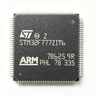
STM32F103ZGT6TR - 72MHz Cortex-M3 1MB Flash MCU | ST | Industrial (Tape & Reel)
MPN: STM32F103ZGT6TR ✓ AktifSTM32F103ZGT6TR Ringkasan
A microcontroller (MCU) is a single-chip embedded computer that integrates a processor core, memory, and peripherals on one die, sitting at the device level of the embedded systems hierarchy (MCU -> embedded processor -> semiconductor). The STM32F103 family, based on the ARM Cortex-M3 RISC architecture, is one of the most widely adopted 32-bit MCU platforms in industrial and consumer electronics, supported by an extensive tool ecosystem including STM32CubeIDE, Keil MDK, and IAR Embedded Workbench.
Key features include 1 MB on-chip Flash with 96 KB SRAM, three 12-bit ADCs, ten general-purpose 16-bit timers plus two advanced PWM timers (17 timers in total), and 13 communication interfaces covering USB 2.0 full-speed, CAN 2.0B, multiple USARTs, SPI and I2C ports. According to the STMicroelectronics datasheet, the Cortex-M3 core delivers 1.25 DMIPS/MHz (Dhrystone 2.1), enabling deterministic real-time control.
Technically, the XL-density devices add a FSMC (flexible static memory controller) for external memories and LCDs, a dual-SPI and SDIO interface, and an extensive DMA controller that offloads data movement from the CPU. The nested vectored interrupt controller (NVIC) provides low-latency interrupt handling essential for motor control and real-time I/O.
Typical applications include industrial motor control, communication boards and gateways, medical instrumentation, and consumer appliances. The rich timer and PWM resources fit three-phase inverter drives, while USB and CAN interfaces suit fieldbus nodes and HID devices.
Design consideration: power the MCU from a 2.0 V to 3.6 V supply and decouple each VDD pin with 100 nF ceramics; Flash wait states must be set to two at 72 MHz for 3.3 V operation.
This page synthesizes distributor pricing, pin-to-pin alternatives (including GD32F103), and practical design notes not found in the manufacturer datasheet.
Pilihan pengganti yang segera untuk STM32F103ZGT6TR — sama paket, pin-pin kompatibel. Bahagian paket yang berbeza memerlukan kerja ulang PCB diasingkan.
Varietas dalam siri ini
Model serupa yang kompatibel dengan pengganti yang segera STM32F103ZGT6TR (sama faktor bentuk dan kaki) — berbeza dalam Communication Interfaces, Package, Timers, ADC Resolution, CAN.
STM32F103ZCT6
✅ Masuk Drop-InHubungi untuk harga
Lihat Datasheet →STM32F103ZET6
✅ Masuk Drop-In ⚠️ Spesifikasi Tidak Disahkan✗ Stok Habis
$5.39 / Unit
Lihat Datasheet →GD32F103ZGT6
✅ Masuk Drop-In📋 Alternatif rujukan (tidak dalam katalog)
APM32F103ZGT6
✅ Masuk Drop-In📋 Alternatif rujukan (tidak dalam katalog)
CKS32F103ZGT6
✅ Masuk Drop-In📋 Alternatif rujukan (tidak dalam katalog)
MM32F103ZGT6
✅ Masuk Drop-In📋 Alternatif rujukan (tidak dalam katalog)
STM32F103ZGT6TR Penilaian maksimum & Ciri-ciri Elektrik
| Core | ARM Cortex-M3 32-bit |
| Frekuensi Klock Maksimum | 72 MHz |
| Core Performance | 1.25 DMIPS/MHz (Dhrystone 2.1) |
| Flash Memory | 1 MB (1M x 8) |
| Kemasan | LQFP-144 (20x20 mm) |
| Jenis Pemasangan | Surface Mount |
| ADCs | 3 x 12-bit |
| Timers | 10 x general-purpose 16-bit + 2 x PWM (17 total) |
| Communication Interfaces | 13 (USB, CAN, USART, SPI, I2C, SDIO) |
| USB | USB 2.0 full-speed |
| CAN | 2.0B |
| Series | STM32F1 (XL-density performance line) |
| External Memory Controller | FSMC |
Panduan Konfigurasi Pin STM32F103ZGT6TR lqfp-144 (20x20 mm)
Konfigurasi pin untuk STM32F103ZGT6TR (lqfp-144 (20x20 mm) pakai). IC digital ini termasuk GPIO, antaramuka komunikasi (UART, SPI, I2C), dan pin kuasa. Rujuk dokumen pengeluar untuk fungsi pin alternatif dan opsi konfigurasi. Biasa digunakan dalam rancangan sistem ter嵌入式 dan PCB.
Tiada data garisan pin yang diperoleh untuk STM32F103ZGT6TR.
Rujuk kepada lembaran data untuk konfigurasi pin penuh.
Aplikasi Biasa
STM32F103ZGT6TR patut untuk 6 aplikasis: Industrial Motor Control, Industrial Communication Gateways, USB Instruments and HIDs, HMI and Display Control, Medical and Test Instrumentation, IoT Sensor Nodes and Smart Devices.
Industrial Motor Control
The STM32F103ZGT6TR fits three-phase BLDC and PMSM inverter drives because its two advanced PWM timers generate complementary outputs with programmable dead-time and break inputs, while its three 12-bit ADCs sample phase currents and bus voltage with fast conversion times. Running at 72 MHz / 1.25 DMIPS/MHz, the Cortex-M3 core executes field-oriented control loops with deterministic interrupt latency via the NVIC. In typical use, the MCU sits between a gate-driver stage and current-sense shunts, issuing six PWM channels at 16-20 kHz carrier frequency. The trade-off versus dedicated motor-assist ICs is greater firmware flexibility for sensorless algorithms at the cost of CPU headroom for the control loop.
Disebarkan
Industrial Communication Gateways
With 13 communication interfaces including USB 2.0 full-speed, bxCAN 2.0B, multiple USARTs, SPI, and I2C, the STM32F103ZGT6TR acts as a protocol bridge in factory automation and building control. A typical deployment translates CAN fieldbus traffic to Modbus RTU over RS-485, using DMA channels to offload byte movement from the CPU while the Cortex-M3 core runs protocol stacks in its 1 MB Flash. The FSMC can additionally buffer frames in external SRAM. The Z-package's large GPIO count (112 I/O lines) supports multi-port designs without an external multiplexer, and hardware CAN filtering reduces interrupt load in high-traffic networks.
Disebarkan
USB Instruments and HIDs
The STM32F103ZGT6TR integrates a USB 2.0 full-speed device controller, making it a common choice for USB-connected measurement pods, debug probes (many popular open-source debuggers are F103-based), and custom HID devices. Its 72 MHz core handles enumeration, endpoint servicing, and signal processing concurrently, while 1 MB Flash holds USB stacks plus application firmware and optional mass-storage or bootloader images. Combined with its 12-bit ADCs, the part supports simple data-acquisition dongles streaming over USB bulk endpoints. Designers must supply a stable 48 MHz USB clock from the PLL and meet USB signal-integrity routing rules on the DP/DM pair.
Disebarkan
HMI and Display Control
The FSMC external memory controller of the STM32F103ZGT6TR memory-maps LCD panel frame buffers and NOR Flash, allowing parallel-interface TFT modules up to mid-size resolutions to be driven without serial bottlenecks. With 96 KB SRAM for double buffering and DMA-assisted transfers, the MCU sustains smooth UI updates while the 1 MB Flash stores font sets, images, and application logic. Typical circuits connect the FSMC 16-bit data bus to an LCD controller such as ILI9341 with a touch controller on SPI. The trade-off versus application processors is far lower cost and power, at the expense of limited animation performance for complex graphics.
Disebarkan
Medical and Test Instrumentation
Three 12-bit ADCs with multiple trigger sources, a precise timer suite, and a 72 MHz Cortex-M3 core make the STM32F103ZGT6TR suitable for portable medical and bench instruments such as patient-side monitors, blood-pressure modules, and handheld data loggers. Its deterministic interrupt behavior supports time-critical sampling schedules, while the CAN and USB interfaces forward data to clinic networks or PCs. The -40C to +85C industrial temperature grade of the T6 suffix covers harsh storage and transport conditions, and the 2.0-3.6 V supply range permits battery operation with a single Li-ion cell through a small regulator. Long software lifecycle support protects multi-year medical product programs.
Disebarkan
IoT Sensor Nodes and Smart Devices
For connected sensing nodes, the STM32F103ZGT6TR pairs with external radio modules (Wi-Fi, LoRa, or Zigbee) over USART/SPI while its abundant GPIOs and ADC channels acquire sensor data locally. The 1 MB Flash hosts firmware, a lightweight IP or LoRaWAN stack, and an over-the-air update bootloader, and 96 KB SRAM accommodates TLS buffers where secure uplinks are required. The Cortex-M3 sleep and stop modes reduce average power draw in battery-powered deployments, though ultra-low-power designs should evaluate the STM32L series instead. Its wide tool support, low unit cost at volume, and second-source alternatives (GD32F103) ease long-term procurement for consumer IoT platforms.
Disebarkan
Ringkasan Produk Disebarkan
Data referensi kejuruteraan untuk STM32F103ZGT6TR — perbandingan, panduan rancangan, dan maklumat kesediaan
Panduan Pilihan
Perbandingan dengan Gantian
| Parametr | Produk Ini | STM32F103ZCT6 | STM32F103ZET6 | GD32F103ZGT6 | APM32F103ZGT6 |
|---|---|---|---|---|---|
| Package | LQFP-144 (20x20 mm) | LQFP-144 (20x20 mm) - same | LQFP-144 (20x20 mm) - same | LQFP-144 (20x20 mm) - same | LQFP-144 (20x20 mm) - same |
| Brand | STMicroelectronics | STMicroelectronics | STMicroelectronics | GigaDevice | Geehy Semiconductor |
| Core | ARM Cortex-M3, 72 MHz | ARM Cortex-M3, 72 MHz | ARM Cortex-M3, 72 MHz | ARM Cortex-M3, up to 108 MHz | ARM Cortex-M3, 72 MHz |
| Flash Memory | 1 MB | 768 KB | 512 KB | 1 MB | 1 MB |
| SRAM | 96 KB | 96 KB | 64 KB | 96 KB | 96 KB |
| Communication Interfaces | 13 (USB, CAN, USART, SPI, I2C) | 13 - same | 13 - same | comparable set, USB/CAN/USART/SPI/I2C | comparable set |
| Timers | 17 (10 GP 16-bit + 2 PWM) | 17 - same | 17 - same | comparable | comparable |
| ADCs | 3 x 12-bit | 3 x 12-bit | 3 x 12-bit | 3 x 12-bit | 3 x 12-bit |
Penyeberangsung Jelas
- Maximum memory in the STM32F103 family (vsSTM32F103ZCT6)
- 96 KB SRAM (vsSTM32F103ZET6)
- Guaranteed ST ecosystem and documented errata (vsGD32F103ZGT6)
- Trade-off: cost and speed (vsGD32F103ZGT6)
Catatan Desain
Power VDD/VDDA from a 2.0 V to 3.6 V rail (3.3 V typical). Decouple every VDD pin pair with 100 nF ceramics placed within 2 mm of the pin, plus one 4.7-10 uF bulk capacitor per supply domain. Keep VDDA on a separate filtered supply (ferrite bead + 1 uF + 10 nF) because ADC accuracy degrades with digital rail noise. Estimated: at 72 MHz with peripherals active, core current is on the order of 36-50 mA (typical F1 figures), so a 100 mA LDO margin suffices for the MCU alone; budget separately for I/O loads.
For the 144-pin LQFP, breakout the fine 0.5 mm pitch with via-in-pad or dog-bone fanout on a minimum 4-layer stack (signal-ground-power-signal) to guarantee return paths. Route the USB DP/DM pair as a 90-ohm differential with length matching better than 1 mm and no stubs. Place the 8 MHz crystal within 5 mm of OSC pins with guard ground, and keep the NRST trace short with a 100 nF capacitor. Unused GPIOs should be configured as analog inputs or outputs-low per ST errata guidance to reduce consumption.
Set Flash latency (wait states) to 2 at 72 MHz and 3.3 V, or code will run unreliably - the most common STM32F1 bring-up failure. If migrating firmware to GD32F103 or other pin-compatible alternatives, re-time delay loops and Flash-dependent code because Flash access timing differs (GD32 is zero-wait-state), which breaks cycle-count-accurate bit-banging and some bootloaders. Also verify JTAG/SWD pin remapping (PA13/PA15, PB3/PB4 default to debug functions) before reclaiming them as GPIO, and connect BOOT0 logic correctly for user-Flash boot.
Maklumat Kesediaan
Compliance status not stated in the provided verified web data; the 'T6' suffix denotes -40C to +85C industrial temperature grade in an LQFP package. Verify RoHS/REACH status on the ST product page for the exact ordering code.