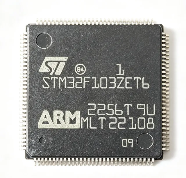
STM32F103ZET6 - 72MHz Cortex-M3 MCU 512KB Flash | STMicroelectronics
MPN: STM32F103ZET6 ✓ Active| Qty | Unit Price | Extended |
|---|---|---|
| 1 | $8.42 | $8.42 |
| 10 | $7.58 | $75.80 |
| 100 | $6.74 | $674.00 |
| 500 | $6.06 | $3,030.00 |
| 1,000 | $5.39 | $5,390.00 |
STM32F103ZET6 Overview
A microcontroller (MCU) is a compact integrated circuit that combines a processor core, memory, and programmable peripherals on a single chip to govern a specific operation in an embedded system. MCUs sit at the heart of the embedded electronics hierarchy - from the ARM Cortex-M processor core, through the STM32 family of 32-bit microcontrollers, up to complete embedded control systems used in industrial automation, consumer devices, and IoT products.
Key features include three 12-bit ADCs with up to 21 channels, two 12-bit DACs, a 12-channel DMA controller, and an unusually rich communication set: up to 5 USARTs, 3 SPIs, 2 I2Cs, 1 CAN 2.0B, 1 USB 2.0 Full-Speed, and 1 SDIO interface. The Cortex-M3 core delivers 1.25 DMIPS/MHz (Dhrystone 2.1), giving roughly 90 DMIPS at 72 MHz, while the Nested Vectored Interrupt Controller (NVIC) provides low-latency deterministic interrupt handling.
Architecturally, the device integrates advanced-control, general-purpose, and basic timers (including PWM timers for motor control), a real-time clock (RTC), and a CRC calculation unit. Both JTAG and Serial Wire Debug (SWD) interfaces are supported, and boot can be selected from Flash, system memory, or SRAM. The 512 KB Flash and 112 GPIOs of the LQFP144 make it the largest-pin, largest-memory STM32F103 variant, ideal for complex firmware with real-time control and multiple communication stacks.
Typical applications include industrial control and PLC systems, motor drives, medical devices, communication boards, and IoT gateways. The wide 2.0 V to 3.6 V supply range and -40C to +85C operating temperature support both battery-powered and industrial designs.
When designing with this device, decouple every VDD pin with 100 nF ceramic capacitors placed close to the pins plus one bulk capacitor, and filter VDDA with a ferrite bead to protect the 12-bit ADC noise floor. The BOOT0/BOOT1 pins must be strapped correctly at reset to select the desired boot source.
This page adds value beyond the ST datasheet by synthesizing drop-in alternatives (GD32F103ZET6, APM32E103ZET6), pricing tiers, engineering design notes, and application guidance in one citable reference.
Drop-in alternatives for STM32F103ZET6 — same package, pin-to-pin compatible. Different-package parts requiring PCB rework are excluded.
Variants in this series
Same-series models that are drop-in compatible with STM32F103ZET6 (same form factor and footprint) — differing in Timers, Package, Communication Interfaces, Flash Memory, Operating Temperature.
Quick Comparison Tool — Select alternative parts for side-by-side comparison:
STM32F103ZGT6
✅ Drop-In✓ In Stock
$5.4 / Unit
View Datasheet →STM32F103ZCT6
✅ Drop-In✓ In Stock
Contact for price
View Datasheet →STM32F103Z8T6
✅ Drop-In✓ In Stock
$3.55 / Unit
View Datasheet →GD32F103ZET6
✅ Drop-In📋 Reference alternative (not in catalog)
APM32E103ZET6
✅ Drop-In📋 Reference alternative (not in catalog)
STM32F103ZET6 Maximum Ratings & Electrical Characteristics
| Core Processor | ARM Cortex-M3 32-bit RISC |
| Maximum Clock Frequency | 72 MHz |
| Core Performance | 1.25 DMIPS/MHz (Dhrystone 2.1) |
| Program Memory Size | 512 KB Flash |
| SRAM Size | 64 KB |
| Supply Voltage Range | 2.0 V to 3.6 V |
| Number of GPIOs | 112 |
| ADC Resolution | 12-bit, 3 ADCs, up to 21 channels |
| DAC Resolution | 12-bit, 2 channels |
| DMA Channels | 12 |
| Communication Interfaces | 5 USART, 3 SPI, 2 I2C, 1 CAN 2.0B, 1 USB 2.0 FS, 1 SDIO |
| Timers | Advanced-control, general-purpose and basic timers plus RTC |
| Package | LQFP-144 (20 x 20 mm) |
| Operating Temperature | -40C to +85C |
| Debug Interface | JTAG and Serial Wire Debug (SWD) |
| Boot Sources | Flash, system memory, or SRAM |
| Mounting Type | Surface Mount |
| RoHS Status | Compliant |
STM32F103ZET6 Pin Configuration
| Pin 1 | PE2 — GPIO port E bit 2 |
| Pin 2 | PE3 — GPIO port E bit 3 |
| Pin 3 | PE4 — GPIO port E bit 4 |
| Pin 4 | PE5 — GPIO port E bit 5 |
| Pin 5 | PE6 — GPIO port E bit 6 |
| Pin 6 | VBAT — Backup battery supply for RTC and backup registers |
| Pin 7 | PC13 — GPIO port C bit 13 / tamper / RTC |
| Pin 8 | PC14 — GPIO port C bit 14 / OSC32_IN |
| Pin 9 | PC15 — GPIO port C bit 15 / OSC32_OUT |
| Pin 10 | PD0 — GPIO port D bit 0 / OSC_IN |
| Pin 11 | PD1 — GPIO port D bit 1 / OSC_OUT |
| Pin 12 | PD2 — GPIO port D bit 2 / SDIO_CMD |
| Pin 13 | PD3 — GPIO port D bit 3 / USART2_CTS |
| Pin 14 | PD4 — GPIO port D bit 4 / USART2_RTS |
| Pin 15 | PD5 — GPIO port D bit 5 / USART2_TX |
| Pin 16 | PD6 — GPIO port D bit 6 / USART2_RX |
| Pin 17 | PD7 — GPIO port D bit 7 / USART2_CK |
| Pin 18 | PD8 — GPIO port D bit 8 / USART3_TX |
| Pin 19 | PD9 — GPIO port D bit 9 / USART3_RX |
| Pin 20 | PD10 — GPIO port D bit 10 / USART3_CK |
| Pin 21 | PD11 — GPIO port D bit 11 / USART3_CTS |
| Pin 22 | PD12 — GPIO port D bit 12 / USART3_RTS |
| Pin 23 | PD13 — GPIO port D bit 13 |
| Pin 24 | PD14 — GPIO port D bit 14 |
| Pin 25 | PD15 — GPIO port D bit 15 |
| Pin 26 | PG0 — GPIO port G bit 0 |
| Pin 27 | PG1 — GPIO port G bit 1 |
| Pin 28 | PG2 — GPIO port G bit 2 |
| Pin 29 | PG3 — GPIO port G bit 3 |
| Pin 30 | PG4 — GPIO port G bit 4 |
| Pin 31 | PG5 — GPIO port G bit 5 |
| Pin 32 | PG6 — GPIO port G bit 6 |
| Pin 33 | PG7 — GPIO port G bit 7 |
| Pin 34 | PG8 — GPIO port G bit 8 |
| Pin 35 | PG9 — GPIO port G bit 9 |
| Pin 36 | PG10 — GPIO port G bit 10 |
| Pin 37 | PG11 — GPIO port G bit 11 |
| Pin 38 | PG12 — GPIO port G bit 12 |
| Pin 39 | PG13 — GPIO port G bit 13 |
| Pin 40 | PG14 — GPIO port G bit 14 |
| Pin 41 | PG15 — GPIO port G bit 15 |
| Pin 42 | PB0 — GPIO port B bit 0 / ADC12_IN8 |
| Pin 43 | PB1 — GPIO port B bit 1 / ADC12_IN9 |
| Pin 44 | PB2 — GPIO port B bit 2 / BOOT1 |
| Pin 45 | PB3 — GPIO port B bit 3 / JTDO |
| Pin 46 | PB4 — GPIO port B bit 4 / NJTRST |
| Pin 47 | PB5 — GPIO port B bit 5 |
| Pin 48 | PB6 — GPIO port B bit 6 / I2C1_SCL |
| Pin 49 | PB7 — GPIO port B bit 7 / I2C1_SDA |
| Pin 50 | PB8 — GPIO port B bit 8 / CAN_RX |
| Pin 51 | PB9 — GPIO port B bit 9 / CAN_TX |
| Pin 52 | PB10 — GPIO port B bit 10 / I2C2_SCL |
| Pin 53 | PB11 — GPIO port B bit 11 / I2C2_SDA |
| Pin 54 | PB12 — GPIO port B bit 12 / SPI2_NSS |
| Pin 55 | PB13 — GPIO port B bit 13 / SPI2_SCK |
| Pin 56 | PB14 — GPIO port B bit 14 / SPI2_MISO |
| Pin 57 | PB15 — GPIO port B bit 15 / SPI2_MOSI |
| Pin 58 | PD8 — GPIO port D bit 8 / USART3_TX |
| Pin 59 | PD9 — GPIO port D bit 9 / USART3_RX |
| Pin 60 | PD10 — GPIO port D bit 10 / USART3_CK |
| Pin 61 | PD11 — GPIO port D bit 11 / USART3_CTS |
| Pin 62 | PD12 — GPIO port D bit 12 / USART3_RTS |
| Pin 63 | PD13 — GPIO port D bit 13 |
| Pin 64 | PD14 — GPIO port D bit 14 |
| Pin 65 | PD15 — GPIO port D bit 15 |
| Pin 66 | PC0 — GPIO port C bit 0 / ADC12_IN10 |
| Pin 67 | PC1 — GPIO port C bit 1 / ADC12_IN11 |
| Pin 68 | PC2 — GPIO port C bit 2 / ADC12_IN12 |
| Pin 69 | PC3 — GPIO port C bit 3 / ADC12_IN13 |
| Pin 70 | PC4 — GPIO port C bit 4 / ADC12_IN14 |
| Pin 71 | PC5 — GPIO port C bit 5 / ADC12_IN15 |
| Pin 72 | VSS_1 — Ground |
| Pin 73 | VDD_1 — Digital power supply 2.0 V to 3.6 V |
| Pin 74 | PC6 — GPIO port C bit 6 / TIM3_CH1 |
| Pin 75 | PC7 — GPIO port C bit 7 / TIM3_CH2 |
| Pin 76 | PC8 — GPIO port C bit 8 / TIM3_CH3 |
| Pin 77 | PC9 — GPIO port C bit 9 / TIM3_CH4 |
| Pin 78 | PC10 — GPIO port C bit 10 / USART3_TX |
| Pin 79 | PC11 — GPIO port C bit 11 / USART3_RX |
| Pin 80 | PC12 — GPIO port C bit 12 / USART3_CK |
| Pin 81 | PD0 — GPIO port D bit 0 / OSC_IN |
| Pin 82 | PD1 — GPIO port D bit 1 / OSC_OUT |
| Pin 83 | PD2 — GPIO port D bit 2 / SDIO_CMD |
| Pin 84 | PD3 — GPIO port D bit 3 / USART2_CTS |
| Pin 85 | PD4 — GPIO port D bit 4 / USART2_RTS |
| Pin 86 | PD5 — GPIO port D bit 5 / USART2_TX |
| Pin 87 | PD6 — GPIO port D bit 6 / USART2_RX |
| Pin 88 | PD7 — GPIO port D bit 7 / USART2_CK |
| Pin 89 | PG9 — GPIO port G bit 9 |
| Pin 90 | PG10 — GPIO port G bit 10 |
| Pin 91 | PG11 — GPIO port G bit 11 |
| Pin 92 | PG12 — GPIO port G bit 12 |
| Pin 93 | PG13 — GPIO port G bit 13 |
| Pin 94 | PG14 — GPIO port G bit 14 |
| Pin 95 | PG15 — GPIO port G bit 15 |
| Pin 96 | PB3 — GPIO port B bit 3 / JTDO |
| Pin 97 | PB4 — GPIO port B bit 4 / NJTRST |
| Pin 98 | PB5 — GPIO port B bit 5 |
| Pin 99 | PB6 — GPIO port B bit 6 / I2C1_SCL |
| Pin 100 | PB7 — GPIO port B bit 7 / I2C1_SDA |
| Pin 101 | BOOT0 — Boot mode selection input |
| Pin 102 | PB8 — GPIO port B bit 8 / CAN_RX |
| Pin 103 | PB9 — GPIO port B bit 9 / CAN_TX |
| Pin 104 | PE0 — GPIO port E bit 0 |
| Pin 105 | PE1 — GPIO port E bit 1 |
| Pin 106 | VSS_2 — Ground |
| Pin 107 | VDD_2 — Digital power supply 2.0 V to 3.6 V |
| Pin 108 | PE2 — GPIO port E bit 2 |
| Pin 109 | PE3 — GPIO port E bit 3 |
| Pin 110 | PE4 — GPIO port E bit 4 |
| Pin 111 | PE5 — GPIO port E bit 5 |
| Pin 112 | PE6 — GPIO port E bit 6 |
| Pin 113 | VSS_3 — Ground |
| Pin 114 | VDD_3 — Digital power supply 2.0 V to 3.6 V |
| Pin 115 | PA0 — GPIO port A bit 0 / WKUP / ADC12_IN0 |
| Pin 116 | PA1 — GPIO port A bit 1 / ADC12_IN1 |
| Pin 117 | PA2 — GPIO port A bit 2 / USART2_TX / ADC12_IN2 |
| Pin 118 | PA3 — GPIO port A bit 3 / USART2_RX / ADC12_IN3 |
| Pin 119 | VSS_4 — Ground |
| Pin 120 | VDD_4 — Digital power supply 2.0 V to 3.6 V |
| Pin 121 | PA4 — GPIO port A bit 4 / SPI1_NSS / ADC12_IN4 / DAC_OUT1 |
| Pin 122 | PA5 — GPIO port A bit 5 / SPI1_SCK / ADC12_IN5 / DAC_OUT2 |
| Pin 123 | PA6 — GPIO port A bit 6 / SPI1_MISO / ADC12_IN6 |
| Pin 124 | PA7 — GPIO port A bit 7 / SPI1_MOSI / ADC12_IN7 |
| Pin 125 | PC4 — GPIO port C bit 4 / ADC12_IN14 |
| Pin 126 | PC5 — GPIO port C bit 5 / ADC12_IN15 |
| Pin 127 | PB0 — GPIO port B bit 0 / ADC12_IN8 |
| Pin 128 | PB1 — GPIO port B bit 1 / ADC12_IN9 |
| Pin 129 | PB2 — GPIO port B bit 2 / BOOT1 |
| Pin 130 | PE7 — GPIO port E bit 7 |
| Pin 131 | PE8 — GPIO port E bit 8 |
| Pin 132 | PE9 — GPIO port E bit 9 |
| Pin 133 | PE10 — GPIO port E bit 10 |
| Pin 134 | PE11 — GPIO port E bit 11 |
| Pin 135 | PE12 — GPIO port E bit 12 |
| Pin 136 | PE13 — GPIO port E bit 13 |
| Pin 137 | PE14 — GPIO port E bit 14 |
| Pin 138 | PE15 — GPIO port E bit 15 |
| Pin 139 | PB10 — GPIO port B bit 10 / I2C2_SCL |
| Pin 140 | PB11 — GPIO port B bit 11 / I2C2_SDA |
| Pin 141 | VSS_5 — Ground |
| Pin 142 | VDD_5 — Digital power supply 2.0 V to 3.6 V |
| Pin 143 | PB12 — GPIO port B bit 12 / SPI2_NSS |
| Pin 144 | PB13 — GPIO port B bit 13 / SPI2_SCK |
Typical Applications
STM32F103ZET6 is suitable for 6 applications: Industrial Control and PLC Systems, Motor Drives and Motion Control, Medical Devices and Patient Monitoring, IoT Gateways and Communication Boards, Consumer Appliances and White Goods, Test and Measurement Instrumentation.
Industrial Control and PLC Systems
The STM32F103ZET6 fits industrial PLC and control systems because its 112 GPIOs, 5 USARTs, and CAN 2.0B interface allow direct connection to field I/O modules, encoders, and industrial buses without external glue logic. The 512 KB Flash accommodates ladder-logic interpreters and Modbus stacks, while the 72 MHz Cortex-M3 core executes deterministic scan cycles. In a typical PLC slice, the MCU scans digital inputs through port expanders, drives relay outputs via shift registers, and exchanges data over CAN or RS-485. The 12-bit ADCs sample 4-20 mA sensor loops, and the 12-channel DMA offloads conversion transfers to keep scan jitter low. Unlike a smaller STM32F103 variant, the LQFP-144 package exposes enough pins to avoid multiplexing conflicts between communication peripherals and I/O, simplifying PCB routing in multi-module racks.
Recommended
Motor Drives and Motion Control
The STM32F103ZET6 is used in motor drives because its advanced-control timers generate complementary PWM with dead-time insertion for three-phase inverters, while three 12-bit ADCs with up to 21 channels sample phase currents and DC-link voltage simultaneously. The 12-channel DMA moves ADC results to memory without CPU intervention, preserving bandwidth for field-oriented control math at 72 MHz. In a typical BLDC or PMSM drive, the MCU runs a current loop at 10-20 kHz, a speed loop at 1 kHz, and communicates setpoints over CAN 2.0B or USART. The 512 KB Flash stores motor parameter tables and communication stacks. Compared with lower-pin STM32F103 parts, the LQFP-144 provides enough GPIOs for gate-driver fault inputs, encoder feedback, and user interface without port sharing.
Recommended
Medical Devices and Patient Monitoring
The STM32F103ZET6 suits medical monitoring equipment because its three 12-bit ADCs and two 12-bit DACs support multi-channel biosignal acquisition and analog output calibration, while the 512 KB Flash holds signal-processing firmware and communication protocols. In a patient monitor, the MCU samples ECG or SpO2 front-end outputs through the ADCs, filters them in real time, and streams results over USB 2.0 Full-Speed or USART to a host display. The 112 GPIOs drive status LEDs, buttons, and alarm outputs. The 2.0 V to 3.6 V supply range allows direct operation from a regulated 3.3 V medical rail, and the -40C to +85C temperature range covers clinical environments. Designers should filter VDDA with a ferrite bead and keep analog and digital grounds separated to protect the ADC noise floor.
Recommended
IoT Gateways and Communication Boards
The STM32F103ZET6 is used in IoT gateways because its communication peripheral set - 5 USARTs, 3 SPIs, 2 I2Cs, 1 CAN 2.0B, 1 USB 2.0 Full-Speed, and 1 SDIO - allows simultaneous connection to wireless modules, sensors, and storage without external bridges. In a gateway design, the MCU runs a protocol stack that translates Modbus or CAN field data into MQTT or HTTP payloads forwarded through an external Wi-Fi or cellular module over USART or SPI. The SDIO interface supports local data logging to an SD card, and the 512 KB Flash stores the TCP/IP stack and configuration. The 72 MHz core provides enough throughput for packet parsing and encryption, while the 112 GPIOs accommodate status indicators and module control lines.
Recommended
Consumer Appliances and White Goods
The STM32F103ZET6 fits consumer appliance control because its 112 GPIOs and integrated timers drive multiple loads - motors, heaters, valves, and user-interface panels - from a single MCU, reducing board count. In a washing machine or refrigerator controller, the MCU reads temperature and position sensors through the 12-bit ADCs, drives triacs and relays via GPIO and PWM timers, and manages a display and touch panel over SPI or I2C. The 512 KB Flash stores cycle profiles and safety logic, and the CAN or USART interface supports factory programming and diagnostics. The 2.0 V to 3.6 V supply and -40C to +85C range cover appliance environments. Compared with smaller STM32F103 packages, the LQFP-144 avoids pin multiplexing between the display bus and motor-control timers.
Recommended
Test and Measurement Instrumentation
The STM32F103ZET6 is used in benchtop and portable instruments because its three 12-bit ADCs with up to 21 channels and two 12-bit DACs support multi-point signal acquisition and analog stimulus generation, while the 12-channel DMA sustains high sample rates without CPU stalls. In a data logger or signal analyzer, the MCU samples conditioned inputs, applies digital filtering, and streams results over USB 2.0 Full-Speed to a PC, or logs them to an SD card through the SDIO interface. The 512 KB Flash holds calibration tables and measurement firmware, and the 72 MHz core handles FFT and averaging routines. The 112 GPIOs drive range relays, input multiplexers, and front-panel controls. Designers should keep the analog supply filtered and route ADC inputs away from switching nodes to preserve measurement accuracy.
Recommended
Recommended Products Summary
Engineering reference data for STM32F103ZET6 — comparison, design guidance, and compliance information.
Selection Guide
Comparison with Alternatives
| Parameter | This Product | STM32F103ZGT6 | STM32F103ZCT6 | GD32F103ZET6 | APM32E103ZET6 |
|---|---|---|---|---|---|
| Package | LQFP-144 | LQFP-144 - same | LQFP-144 - same | LQFP-144 - same | LQFP-144 - same |
| Brand | STMicroelectronics | STMicroelectronics | STMicroelectronics | GigaDevice | Geehy |
| Core | ARM Cortex-M3 | ARM Cortex-M3 | ARM Cortex-M3 | ARM Cortex-M3 | ARM Cortex-M3 |
| Max Clock Frequency | 72 MHz | 72 MHz | 72 MHz | 108 MHz | 120 MHz |
| Flash Memory | 512 KB | 1 MB | 256 KB | 512 KB | 512 KB |
| SRAM | 64 KB | 96 KB | 48 KB | 64 KB | 128 KB |
| GPIO Count | 112 | 112 | 112 | 112 | 112 |
| Supply Voltage | 2.0 V to 3.6 V | 2.0 V to 3.6 V | 2.0 V to 3.6 V | 2.6 V to 3.6 V | 2.0 V to 3.6 V |
| CAN Interface | 1x CAN 2.0B | 1x CAN 2.0B | 1x CAN 2.0B | 1x CAN 2.0B | 1x CAN 2.0B |
| USB Interface | 1x USB 2.0 Full-Speed | 1x USB 2.0 Full-Speed | 1x USB 2.0 Full-Speed | 1x USB 2.0 Full-Speed | 1x USB 2.0 Full-Speed |
Key Differentiators
- Largest Flash and GPIO count in the STM32F103 line (vs STM32F103ZCT6)
- Native ST toolchain and ecosystem support (vs GD32F103ZET6)
- Lower clock ceiling than pin-compatible clones (vs APM32E103ZET6)
Design Notes
Decouple every VDD pin (VDD_1 through VDD_5) with a 100 nF ceramic capacitor placed as close to the pin as possible, plus at least one 4.7 uF to 10 uF bulk capacitor near the package. Filter VDDA with a ferrite bead followed by a 100 nF and 1 uF capacitor to protect the 12-bit ADC noise floor. Keep the analog supply within 2.0 V to 3.6 V and ensure VDDA never exceeds VDD by more than 300 mV during power sequencing.
Route the 8 MHz main crystal and 32.768 kHz RTC crystal with short, symmetric traces and guard them with ground. Place the load capacitors close to the crystal pins and avoid routing high-speed signals such as USB or SDIO underneath the oscillator area. For the LQFP-144, use a solid ground plane under the device and connect the exposed thermal pad area with multiple vias if the package variant includes one.
Strap BOOT0 low and BOOT1 (PB2) as required at reset to select boot from Flash; incorrect strapping causes the device to enter the system memory bootloader unexpectedly. Do not leave NRST floating - add a 100 nF capacitor to ground and a 10 kOhm pull-up. When migrating to a GD32F103ZET6 drop-in, re-validate clock configuration and Flash wait states because the clone supports up to 108 MHz with zero-wait Flash buffering.
Compliance Information
RoHS and REACH compliance per STMicroelectronics product page. Not AEC-Q100 qualified - the STM32F103ZET6 is an industrial/consumer grade device rated -40C to +85C.