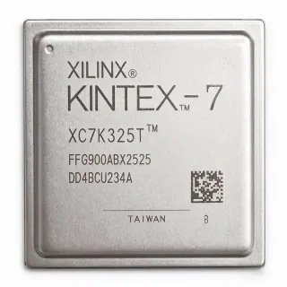
XC7K325T-1FB900C - 326,080-LE Kintex-7 FPGA | AMD
MPN: XC7K325T-1FB900C ✓ AktifXC7K325T-1FB900C Ringkasan
A field-programmable gate array is a semiconductor whose digital logic, interconnects, and peripheral blocks are configured after fabrication. The Kintex-7 family sits between AMD's lower-density programmable-logic products and larger Zynq and Virtex devices. By combining configurable logic with dedicated DSP, memory, and high-speed I/O resources, an FPGA can accelerate parallel processing, signal processing, control, networking, and data-transfer functions without requiring a custom ASIC.
The XC7K325T designation identifies a high-capacity Kintex-7 member. The suffix sequence identifies the -1 performance grade, the FB900 package, and the C temperature designation. The 900-ball FCBGA package supports dense routing to banks of programmable I/O and power-management resources. This package is intended primarily for advanced boards with careful ball assignment, multilayer routing, and controlled power delivery.
The Kintex-7 architecture combines programmable logic with high-speed serial transceivers, dedicated DSP slices, block RAM, and general-purpose I/O. This resource mix allows designers to implement multiple data paths in parallel while retaining specialized hardware for serial interfaces and arithmetic-heavy processing. AMD describes the family as delivering strong price/performance/watt characteristics at the 28 nm process node.
Typical applications include high-throughput data acquisition, industrial control, test and measurement, network packet processing, video and image pipelines, communications infrastructure, and embedded signal-processing systems. The 326,080 logic cells make the device appropriate for designs where parallel logic density is more valuable than minimizing package size or cost. PCIe Gen3 and 10 Gigabit Ethernet support also align it with modern data-plane and host-interface designs.
Hardware implementation requires careful attention to decoupling, power sequencing, clocking, and high-speed signal integrity. Use the pinout files and device documentation to assign power balls, connect all required supplies, and route each high-speed differential pair as a controlled-impedance network. Differential pairs should remain continuous, with matching reference planes and minimal stubs to preserve signal quality.
This product page combines the exact ordering information, 326,080-logic-cell capacity, 900-BBGA package, 28 nm process generation, supported connectivity standards, drop-in family alternatives, and practical PCB implementation guidance. It is designed to accelerate component selection, schematic review, PCB planning, and replacement assessment for engineers working with high-capacity Kintex-7 systems.
Pilihan pengganti yang segera untuk XC7K325T-1FB900C — sama paket, pin-pin kompatibel. Bahagian paket yang berbeza memerlukan kerja ulang PCB diasingkan.
Varietas dalam siri ini
Model serupa yang kompatibel dengan pengganti yang segera XC7K325T-1FB900C (sama faktor bentuk dan kaki) — berbeza dalam Device Type, Package, RoHS Status.
XC7K325T-1FB900I
✅ Masuk Drop-InHubungi untuk harga
Lihat Datasheet →XC7K325T-2FB900C
✅ Masuk Drop-In ⚠️ Spesifikasi Tidak Disahkan📋 Alternatif rujukan (tidak dalam katalog)
XC7K325T-3FB900C
✅ Masuk Drop-In ⚠️ Spesifikasi Tidak Disahkan📋 Alternatif rujukan (tidak dalam katalog)
XC7K325T-1LFB900C
✅ Masuk Drop-In ⚠️ Spesifikasi Tidak Disahkan📋 Alternatif rujukan (tidak dalam katalog)
XC7K325T-2LFB900C
✅ Masuk Drop-In ⚠️ Spesifikasi Tidak Disahkan📋 Alternatif rujukan (tidak dalam katalog)
XC7K325T-1FB900C Penilaian maksimum & Ciri-ciri Elektrik
| Device Type | Kintex-7 field-programmable gate array (FPGA) |
| Logic Cells | 326,080 LEs |
| Process Technology | 28 nm |
| Speed Grade | -1 |
| Kemasan | 900-BBGA, FCBGA |
| Number of Terminals | 900 balls |
| Package Shape | Square |
| High-Speed Serial Support | PCIe Gen3 and 10 Gigabit Ethernet |
| Programmable Logic | 326,080 LEs |
| Family Architecture | Kintex-7 |
| Device Configuration | Field-programmable logic, interconnect, and I/O |
| Temperature Designation | C suffix |
| Status RoHS | unknown |
| REACH Status | unknown |
| AEC-Q100 Qualification | not_applicable |
Panduan Konfigurasi Pin XC7K325T-1FB900C square
Konfigurasi pin untuk XC7K325T-1FB900C (square pakai). IC digital ini termasuk GPIO, antaramuka komunikasi (UART, SPI, I2C), dan pin kuasa. Rujuk dokumen pengeluar untuk fungsi pin alternatif dan opsi konfigurasi. Biasa digunakan dalam rancangan sistem ter嵌入式 dan PCB.

Tiada data garisan pin yang diperoleh untuk XC7K325T-1FB900C.
Rujuk kepada lembaran data untuk konfigurasi pin penuh.
Aplikasi Biasa
XC7K325T-1FB900C patut untuk 6 aplikasis: 10 Gigabit Ethernet Packet Processing, PCIe Gen3 Data-Acquisition Interface, Digital Signal Processing Accelerator, Industrial Control and Automation, Test and Measurement Instrumentation, Video and Image Processing Pipelines.
10 Gigabit Ethernet Packet Processing
The XC7K325T-1FB900C fits parallel packet-processing engines because its 326,080 logic cells can support multiple parsing, classification, queue-management, and forwarding stages at once. AMD identifies 10 Gigabit Ethernet as a mainstream Kintex-7 connectivity option. Designers can pair high-speed transceivers with programmable I/O and dedicated DSP resources while implementing buffering and control logic in the fabric. The principal consideration is power: sustained line-rate operation can make I/O and dynamic power significant, so board thermal design should reflect realistic traffic rather than idle activity.
Disebarkan
PCIe Gen3 Data-Acquisition Interface
The XC7K325T-1FB900C is appropriate for a PCIe Gen3 data-acquisition front end that must transfer high-volume samples into parallel FPGA logic. Its 326,080 logic cells support acquisition formatting, trigger handling, buffering, and real-time processing without relying entirely on external processors. The Kintex-7 family's PCIe Gen3 support makes the device relevant to host-connected instrumentation and test systems. Engineers should reserve lane placement for short, impedance-controlled routing and verify transmitter and receiver equalization against the complete channel and connector environment.
Disebarkan
Digital Signal Processing Accelerator
The XC7K325T-1FB900C can accelerate filters, correlation, modulation, and fixed-point algorithms by combining 326,080 programmable logic cells with the Kintex-7 family's DSP resources. Parallel data paths allow multiple sample lanes or channels to be processed concurrently, while block RAM supports local buffering and coefficient storage. The -1 grade provides a defined timing class for design planning, although each pipeline stage still requires static timing closure. Power analysis should include toggling rate and active DSP resources because arithmetic-heavy designs can consume substantially more dynamic power than control-only logic.
Disebarkan
Industrial Control and Automation
The XC7K325T-1FB900C is suitable for industrial controllers requiring deterministic parallel logic, extensive programmable I/O, and communication interfaces in a single package. A Kintex-7 implementation can combine motion sequencing, machine vision preprocessing, safety-adjacent monitoring, and protocol handling without multiple programmable devices. The XC7K325T-1FB900I offers the same -1 performance class with an industrial temperature designation when the enclosure requires a wider environmental range. Board design must preserve the separation required by the factory's power, isolation, and functional-safety architecture.
Disebarkan
Test and Measurement Instrumentation
The XC7K325T-1FB900C supports parallel acquisition, pattern generation, real-time analysis, and high-speed data movement in advanced instrumentation. The 326,080-logic-cell capacity allows multiple signal-processing channels to coexist, while the 900-BBGA package provides substantial ball access for clocks, data buses, triggers, and serial links. Timing-closure margins depend on the selected -1 grade, so critical interfaces should be constrained according to the AMD Kintex-7 data sheet. Thermal analysis should cover sustained acquisition workloads because continuously active registers and DSPs can raise junction temperature.
Disebarkan
Video and Image Processing Pipelines
The XC7K325T-1FB900C is well matched to parallel image-processing pipelines that require line buffers, filtering, color conversion, feature extraction, and frame-level control. Its 326,080 logic cells provide substantial parallel capacity, while Kintex-7 DSP and memory resources can reduce the amount of general logic required by arithmetic operations. The 900-ball package offers many programmable I/O connections for video interfaces, although high-speed source-synchronous routing demands careful length matching and reference-plane continuity. System power should be estimated using realistic frame rates and active-pixel percentages rather than typical laboratory toggling.
Disebarkan
Ringkasan Produk Disebarkan
Data referensi kejuruteraan untuk XC7K325T-1FB900C — perbandingan, panduan rancangan, dan maklumat kesediaan
Panduan Pilihan
Perbandingan dengan Gantian
| Parametr | Produk Ini | XC7K325T-1FB900I | XC7K325T-2FB900C | XC7K325T-3FB900C | XC7K325T-1LFB900C | XC7K325T-2LFB900C |
|---|---|---|---|---|---|---|
| Brand | AMD | AMD | AMD | AMD | AMD | AMD |
| Package | 900-BBGA (FCBGA) | 900-BBGA (FCBGA) | 900-BBGA (FCBGA) | 900-BBGA (FCBGA) | 900-BBGA (FCBGA) | 900-BBGA (FCBGA) |
| Device Family | Kintex-7 | Kintex-7 | Kintex-7 | Kintex-7 | Kintex-7 | Kintex-7 |
| Logic Cells | 326,080 LEs | 326,080 LEs | 326,080 LEs | 326,080 LEs | 326,080 LEs | 326,080 LEs |
| Speed Grade | -1 | -1 | -2 | -3 | -1L | -2L |
| Temperature Designation | C | I | C | C | C | C |
| Process Technology | 28 nm | 28 nm | 28 nm | 28 nm | 28 nm | 28 nm |
| High-Speed Interface Support | PCIe Gen3 and 10 Gigabit Ethernet | PCIe Gen3 and 10 Gigabit Ethernet | PCIe Gen3 and 10 Gigabit Ethernet | PCIe Gen3 and 10 Gigabit Ethernet | PCIe Gen3 and 10 Gigabit Ethernet | PCIe Gen3 and 10 Gigabit Ethernet |
| Specialized Resource Capacity | Dedicated DSP and memory resources | Dedicated DSP and memory resources | Dedicated DSP and memory resources | Dedicated DSP and memory resources | Dedicated DSP and memory resources | Dedicated DSP and memory resources |
Penyeberangsung Jelas
- High-density programmable logic capacity (vsXC7K325T-1FB900I)
- Choice of speed grade without changing the FB900 footprint (vsXC7K325T-2FB900C)
- Commercial C designation for the target configuration (vsXC7K325T-1FB900I)
- Mainstream high-speed connectivity in the Kintex-7 family (vsXC7K325T-1LFB900C)
Catatan Desain
Use the official FB900 package files as the controlling source for ball assignment, power connections, and PCB footprint design. A 900-BBGA device requires dense escape routing, multilayer power planes, and careful component placement around the FPGA. Assign every power and ground ball exactly as directed by AMD, preserve the documented package geometry, and validate the stencil, solder mask, and land pattern against the current package drawing before fabrication.
Plan the power network around every required supply, its decoupling, and the documented sequencing behavior. Place bulk and high-frequency decoupling near the associated balls rather than relying on remote supply traces to suppress package transients. Verify steady-state and worst-case dynamic current using realistic clock, I/O, DSP, and memory activity. The -1 and -L grades can have different power characteristics, so replacement qualification must include more than a pinout comparison.
Route high-speed serial interfaces as short, continuous differential pairs over a solid reference plane. Avoid plane changes, stubs, unnecessary vias, and breaks beneath the pair, and apply the package and board constraints specified by AMD's PCB guidelines. For source-synchronous and memory interfaces, use length matching and flyaway or compensation structures where the interface timing requires them. Signal-integrity simulation should include realistic connector, package, and via models.
Estimate junction temperature from actual workload rather than nominal device power alone. Include FPGA core activity, transceiver use, DSP loading, I/O switching, board copper, airflow, and adjacent heat sources. A high-density 900-BBGA package may require a multilayer PCB with an uninterrupted copper area and deliberate thermal vias. Validate the finished assembly across ambient and power corners before approving the mechanical design.
Do not treat a same-family suffix change as automatically harmless. XC7K325T-1FB900I changes the environmental designation, while -2, -3, -1L, and -2L alternatives change speed, power, or operating conditions. Before substituting any device, verify the complete ordering code, configuration compatibility, pinout, supply requirements, timing grade, temperature class, and system constraints. A successful PCB fit does not by itself establish functional equivalence.
Maklumat Kesediaan
No specific RoHS, REACH, lead-free, halogen-free, or conflict-minerals status is stated for this ordering code. AEC-Q100 is not applicable because the device is an FPGA rather than an automotive-qualified component.