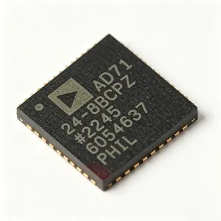
AD5372BSTZ - 32-Channel 16-Bit Serial DAC | Analog Devices
MPN: AD5372BSTZ ✓ Active| Qty | Unit Price | Extended |
|---|---|---|
| 1 | $74.64 | $74.64 |
| 10 | $68.5 | $685.00 |
| 100 | $62 | $6,200.00 |
| 500 | $55 | $27,500.00 |
| 1,000 | $48 | $48,000.00 |
AD5372BSTZ Overview
A digital-to-analog converter (DAC) is an electronic component that converts digital binary data into an analog voltage or current. The AD5372BSTZ belongs to the family of voltage-output DACs, which are essential in applications requiring precise analog control from digital systems, such as industrial automation, instrumentation, and communication systems. As a multi-channel DAC, it integrates 32 individual converters in a single package, reducing board space and simplifying system design.
Key features of the AD5372BSTZ include 16-bit resolution, 32 independent DAC channels, and a serial interface compatible with SPI/QSPI/MICROWIRE. Each DAC has a buffered output capable of driving loads directly, and the gain and offset of each channel can be independently trimmed to remove system errors. The device operates from a single 2.5V to 5.5V supply, with a reference voltage range of 2V to 5V, and provides a nominal output span of 4× VREF.
The AD5372BSTZ uses a resistor-string architecture with an output buffer for each channel, ensuring monotonicity and low glitch energy. The serial interface supports daisy-chaining, allowing multiple devices to be controlled with a single data line. The device includes a power-on reset that clears all DAC registers to zero-scale, and a CLR pin that resets outputs to zero-scale or midscale. The LQFP package provides good thermal performance and is suitable for surface-mount assembly.
Typical applications include automatic test equipment (ATE), optical network control, instrumentation, and industrial process control. The 32 channels and 16-bit resolution make it suitable for systems requiring many precise analog outputs, such as multi-axis positioning, programmable voltage sources, and calibration equipment.
When designing with the AD5372BSTZ, ensure adequate decoupling on the AVDD and DVDD supplies, and place the reference decoupling capacitor close to the REFIN pin. The serial clock frequency should be limited to 50 MHz to ensure reliable communication, and the SYNC pin must be held low during data transfer.
Drop-in alternatives for AD5372BSTZ — same package, pin-to-pin compatible. Different-package parts requiring PCB rework are excluded.
Variants in this series
Same-series models that are drop-in compatible with AD5372BSTZ (same form factor and footprint) — differing in Number of Channels, Package, Resolution, Settling Time, Supply Voltage.
Quick Comparison Tool — Select alternative parts for side-by-side comparison:
AD5372BSTZ-REEL
✅ Drop-In📋 Reference alternative (not in catalog)
AD5373BSTZ
✅ Drop-In📋 Reference alternative (not in catalog)
AD5370BSTZ
✅ Drop-In📋 Reference alternative (not in catalog)
AD5372BSTZ Maximum Ratings & Electrical Characteristics
| Resolution | 16 bit |
| Number of Channels | 32 |
| Interface Type | Serial (SPI/QSPI/MICROWIRE) |
| Output Type | Voltage - Buffered |
| Output Span | 4 × VREF |
| Reference Voltage | 2 V to 5 V |
| Supply Voltage | 2.5 V to 5.5 V |
| Integral Nonlinearity (INL) | ±4 LSB (max) |
| Differential Nonlinearity (DNL) | ±1 LSB (max) |
| Settling Time | 16 µs (typ) |
| Operating Temperature Range | -40°C to +85°C |
| Package | 64-lead LQFP (10x10 mm) |
| Mounting Type | Surface Mount |
| RoHS Status | Compliant |
| Lead-Free | Yes |
AD5372BSTZ Pin Configuration
| Pin 1 | VOUT0 — DAC output channel 0 |
| Pin 2 | VOUT1 — DAC output channel 1 |
| Pin 3 | VOUT2 — DAC output channel 2 |
| Pin 4 | VOUT3 — DAC output channel 3 |
| Pin 5 | VOUT4 — DAC output channel 4 |
| Pin 6 | VOUT5 — DAC output channel 5 |
| Pin 7 | VOUT6 — DAC output channel 6 |
| Pin 8 | VOUT7 — DAC output channel 7 |
| Pin 9 | VOUT8 — DAC output channel 8 |
| Pin 10 | VOUT9 — DAC output channel 9 |
| Pin 11 | VOUT10 — DAC output channel 10 |
| Pin 12 | VOUT11 — DAC output channel 11 |
| Pin 13 | VOUT12 — DAC output channel 12 |
| Pin 14 | VOUT13 — DAC output channel 13 |
| Pin 15 | VOUT14 — DAC output channel 14 |
| Pin 16 | VOUT15 — DAC output channel 15 |
| Pin 17 | VOUT16 — DAC output channel 16 |
| Pin 18 | VOUT17 — DAC output channel 17 |
| Pin 19 | VOUT18 — DAC output channel 18 |
| Pin 20 | VOUT19 — DAC output channel 19 |
| Pin 21 | VOUT20 — DAC output channel 20 |
| Pin 22 | VOUT21 — DAC output channel 21 |
| Pin 23 | VOUT22 — DAC output channel 22 |
| Pin 24 | VOUT23 — DAC output channel 23 |
| Pin 25 | VOUT24 — DAC output channel 24 |
| Pin 26 | VOUT25 — DAC output channel 25 |
| Pin 27 | VOUT26 — DAC output channel 26 |
| Pin 28 | VOUT27 — DAC output channel 27 |
| Pin 29 | VOUT28 — DAC output channel 28 |
| Pin 30 | VOUT29 — DAC output channel 29 |
| Pin 31 | VOUT30 — DAC output channel 30 |
| Pin 32 | VOUT31 — DAC output channel 31 |
| Pin 33 | AVDD — Analog supply voltage |
| Pin 34 | DVDD — Digital supply voltage |
| Pin 35 | GND — Ground |
| Pin 36 | REFIN — Reference input |
| Pin 37 | REFOUT — Reference output |
| Pin 38 | SYNC — Serial interface sync (active low) |
| Pin 39 | SCLK — Serial clock input |
| Pin 40 | SDIN — Serial data input |
| Pin 41 | SDO — Serial data output |
| Pin 42 | CLR — Clear all DACs to zero-scale or midscale |
| Pin 43 | LDAC — Load DAC (active low) |
| Pin 44 | RESET — Reset all registers to default |
Typical Applications
AD5372BSTZ is suitable for 6 applications: Automatic Test Equipment (ATE), Optical Network Control, Instrumentation, Industrial Process Control, Medical Equipment, Communication Systems.
Automatic Test Equipment (ATE)
The AD5372BSTZ provides 32 independent 16-bit voltage outputs, ideal for ATE systems requiring multiple precise stimulus signals. Its fast settling time of 16 µs enables high-throughput testing, while the serial interface simplifies connection to FPGA-based controllers. The independent gain and offset trim per channel allows calibration of each output to meet tight system accuracy requirements.
Recommended
Optical Network Control
In optical networking, the AD5372BSTZ can control variable optical attenuators (VOAs) and tunable lasers. Its 32 channels allow monitoring and control of multiple optical channels simultaneously. The low glitch energy and monotonic output ensure stable analog control signals, while the wide output span (4×VREF) provides sufficient voltage range for various actuator interfaces.
Recommended
Instrumentation
The AD5372BSTZ is well-suited for precision instrumentation such as programmable power supplies and waveform generators. Its 16-bit resolution and 32 channels enable generation of multiple accurate analog signals. The serial interface supports daisy-chaining, allowing expansion to more channels without additional microcontroller pins. The device's power-on reset ensures known output states at startup.
Recommended
Industrial Process Control
In industrial process control, the AD5372BSTZ can drive actuators, valves, and setpoints across 32 channels. Its wide supply voltage range (2.5V to 5.5V) and buffered outputs simplify interface to external drivers. The independent gain and offset trim allows calibration of each channel to match sensor characteristics, improving overall system accuracy.
Recommended
Medical Equipment
The AD5372BSTZ is used in medical equipment such as patient monitoring systems and diagnostic devices, where multiple precise analog outputs are required. Its 16-bit resolution ensures fine control of parameters like gain and offset in signal chains. The small LQFP package and serial interface help reduce board space in compact medical devices.
Recommended
Communication Systems
In communication systems, the AD5372BSTZ can be used for bias control of RF amplifiers and tunable filters. Its 32 channels allow independent control of multiple bias points. The low noise and monotonic output ensure stable operation, while the serial interface is compatible with common DSP and FPGA controllers.
Recommended
Recommended Products Summary
Engineering reference data for AD5372BSTZ — comparison, design guidance, and compliance information.
Selection Guide
Comparison with Alternatives
| Parameter | This Product | AD5372BSTZ-REEL | AD5373BSTZ | AD5370BSTZ | AD5372BCPZ |
|---|---|---|---|---|---|
| Package | 64-lead LQFP | 64-lead LQFP | 64-lead LQFP | 64-lead LQFP | 56-lead LFCSP |
| Brand | Analog Devices | Analog Devices | Analog Devices | Analog Devices | Analog Devices |
| Resolution | 16 bit | 16 bit | 14 bit | 16 bit | 16 bit |
| Number of Channels | 32 | 32 | 32 | 40 | 32 |
| Interface | Serial (SPI/QSPI/MICROWIRE) | Serial (SPI/QSPI/MICROWIRE) | Serial (SPI/QSPI/MICROWIRE) | Serial (SPI/QSPI/MICROWIRE) | Serial (SPI/QSPI/MICROWIRE) |
| Output Span | 4 × VREF | 4 × VREF | 4 × VREF | 4 × VREF | 4 × VREF |
| Supply Voltage | 2.5V to 5.5V | 2.5V to 5.5V | 2.5V to 5.5V | 2.5V to 5.5V | 2.5V to 5.5V |
| Settling Time | 16 µs (typ) | 16 µs (typ) | 16 µs (typ) | 16 µs (typ) | 16 µs (typ) |
Key Differentiators
- 32 independent 16-bit DAC channels in a single package (vs AD5370BSTZ)
- Pin-compatible with AD5373BSTZ (14-bit) (vs AD5373BSTZ)
- LQFP package with exposed pad for better thermal performance (vs AD5372BCPZ)
Design Notes
Decouple AVDD and DVDD with 10 µF and 0.1 µF capacitors placed close to the pins. Use separate analog and digital ground planes to minimize noise coupling. The reference input should be decoupled with a 1 µF capacitor to REFIN and GND.
For optimal performance, place the AD5372BSTZ on a PCB with a solid ground plane. Keep the serial interface traces short and avoid routing them near high-speed digital lines. The LQFP package has exposed pads; ensure proper soldering for thermal and mechanical reliability.
Ensure the SYNC pin is held low during data transfer and that SCLK frequency does not exceed 50 MHz. The CLR pin can be used to reset outputs to zero-scale or midscale; tie it high if not used. Avoid floating the RESET pin; connect it to DVDD through a pull-up resistor.
Compliance Information
RoHS compliant per Analog Devices product page. Not AEC-Q100 qualified.