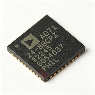
AD7890ANZ-10 - 8-Channel 12-Bit Serial DAS | Analog Devices
MPN: AD7890ANZ-10 ✓ Active| Qty | Unit Price | Extended |
|---|---|---|
| 1 | $18.5 | $18.50 |
| 10 | $16.8 | $168.00 |
| 100 | $14.2 | $1,420.00 |
| 500 | $12.9 | $6,450.00 |
| 1,000 | $11.75 | $11,750.00 |
AD7890ANZ-10 Overview
A data acquisition system (DAS) is a complete signal chain that samples multiple analog signals, converts them to digital, and interfaces with a microcontroller or DSP. The AD7890 integrates the multiplexer, track/hold, ADC, and reference into a single IC, simplifying design and reducing board space compared to discrete implementations. It belongs to the family of serial data acquisition systems, which are essential in industrial automation, process control, and instrumentation.
Key features include a fast 12-bit ADC with 5.9 µs conversion time, eight single-ended analog input channels, and a serial interface compatible with SPI. The on-chip track/hold amplifier ensures accurate sampling of dynamic signals, while the internal 2.5 V reference eliminates the need for external reference circuitry. The multiplexer is independently accessible, allowing users to insert antialiasing filters or signal conditioning between the multiplexer and the ADC.
The AD7890 uses LC2MOS technology, combining low power consumption with high-speed performance. The serial interface supports high-speed data transfer, and the device can be configured for various input ranges (0-2.5 V, 0-4.096 V, ±10 V) depending on the variant. The 24-pin PDIP package is suitable for through-hole assembly, providing ease of prototyping and robust mechanical connection.
Typical applications include industrial process control, data logging, and multi-channel sensor monitoring. The AD7890ANZ-10 is ideal for systems requiring simultaneous sampling of multiple analog signals with 12-bit resolution and serial output for easy microcontroller interfacing.
When designing with this device, ensure proper decoupling of the 5 V supply and careful layout of the analog input traces to minimize noise. The independent multiplexer access allows flexible signal conditioning, but the track/hold acquisition time must be considered for accurate sampling of high-frequency signals.
Drop-in alternatives for AD7890ANZ-10 — same package, pin-to-pin compatible. Different-package parts requiring PCB rework are excluded.
Variants in this series
Same-series models that are drop-in compatible with AD7890ANZ-10 (same form factor and footprint) — differing in Input Voltage Range, Number of Channels, Package, Reference Type, RoHS Status.
Quick Comparison Tool — Select alternative parts for side-by-side comparison:
AD7890BNZ-10
✅ Drop-In📋 Reference alternative (not in catalog)
AD7890AN-10
✅ Drop-In📋 Reference alternative (not in catalog)
AD7890ANZ-10 Maximum Ratings & Electrical Characteristics
| Resolution | 12 bits |
| Number of Channels | 8 single-ended |
| Sampling Rate | 117 kSPS |
| Conversion Time | 5.9 µs |
| Input Voltage Range | ±10 V |
| Supply Voltage | 5 V |
| Interface | SPI |
| Reference Type | Internal 2.5 V |
| Operating Temperature Range | -40°C to +85°C |
| Package | 24-PDIP |
| Mounting Type | Through Hole |
| Screening Level | Industrial |
| RoHS Status | Compliant |
| Technology | LC2MOS |
| Product Category | Data Acquisition ADCs/DACs - Specialized |
AD7890ANZ-10 Pin Configuration
| Pin 1 | VDD — Positive supply voltage (5 V) |
| Pin 2 | VIN1 — Analog input channel 1 |
| Pin 3 | VIN2 — Analog input channel 2 |
| Pin 4 | VIN3 — Analog input channel 3 |
| Pin 5 | VIN4 — Analog input channel 4 |
| Pin 6 | VIN5 — Analog input channel 5 |
| Pin 7 | VIN6 — Analog input channel 6 |
| Pin 8 | VIN7 — Analog input channel 7 |
| Pin 9 | VIN8 — Analog input channel 8 |
| Pin 10 | AGND — Analog ground |
| Pin 11 | REF IN/OUT — Reference input/output (2.5 V) |
| Pin 12 | DGND — Digital ground |
| Pin 13 | SCLK — Serial clock input |
| Pin 14 | SDATA — Serial data output |
| Pin 15 | CS — Chip select (active low) |
| Pin 16 | CONVST — Conversion start input |
| Pin 17 | EOC — End of conversion output |
| Pin 18 | MUXOUT — Multiplexer output (for external conditioning) |
| Pin 19 | MUXIN — Multiplexer input (from conditioning circuit) |
| Pin 20 | A0 — Address input bit 0 |
| Pin 21 | A1 — Address input bit 1 |
| Pin 22 | A2 — Address input bit 2 |
| Pin 23 | STBY — Standby control input |
| Pin 24 | VDD — Positive supply voltage (5 V) |
Typical Applications
AD7890ANZ-10 is suitable for 6 applications: Industrial Process Control, Data Logging Systems, Multi-Channel Sensor Monitoring, Test and Measurement Equipment, Automotive Test Systems, Medical Instrumentation.
Industrial Process Control
The AD7890ANZ-10 is ideal for industrial process control systems that monitor multiple analog signals such as temperature, pressure, and flow. Its 8-channel multiplexer allows sampling of up to eight sensors with a single ADC, reducing component count. The ±10 V input range accommodates standard industrial sensor outputs, and the 12-bit resolution provides adequate precision for control loops. The serial SPI interface simplifies connection to microcontrollers, enabling fast data transfer for real-time monitoring and control. The industrial temperature range (-40°C to +85°C) ensures reliable operation in harsh factory environments.
Recommended
Data Logging Systems
In data logging applications, the AD7890ANZ-10 captures multiple analog channels sequentially and converts them to digital for storage. Its 117 kSPS sampling rate allows logging of dynamic signals with reasonable fidelity. The on-chip track/hold amplifier ensures accurate sampling of varying inputs. The internal 2.5 V reference provides a stable conversion reference, eliminating external components. The serial interface enables easy interfacing with SD cards or wireless modules for remote logging. The low power consumption of LC2MOS technology is beneficial for battery-powered loggers, though the 5 V supply may require a regulator.
Recommended
Multi-Channel Sensor Monitoring
The AD7890ANZ-10 is well-suited for multi-channel sensor monitoring in applications like environmental monitoring or equipment health tracking. Its 8 single-ended inputs can connect to various sensors, including temperature, humidity, and vibration sensors. The ±10 V range supports sensors with bipolar outputs, such as accelerometers. The independent multiplexer access allows insertion of signal conditioning circuits, like filters or amplifiers, between the multiplexer and ADC. This flexibility enables tailored signal processing for each channel. The SPI interface allows a single microcontroller to read all channels sequentially, simplifying system design.
Recommended
Test and Measurement Equipment
The AD7890ANZ-10 is used in test and measurement equipment such as data acquisition cards and portable instruments. Its 12-bit resolution and 117 kSPS sampling rate provide adequate performance for many measurement tasks. The serial interface reduces pin count, allowing compact PCB designs. The ±10 V input range is compatible with common test signals. The industrial temperature range ensures stability in lab and field environments. The on-chip reference simplifies calibration, and the track/hold amplifier ensures accurate sampling of transient signals. This makes it a cost-effective choice for multi-channel measurement systems.
Recommended
Automotive Test Systems
In automotive test systems, the AD7890ANZ-10 can monitor multiple sensors such as throttle position, temperature, and pressure. Its 8-channel input allows simultaneous sampling of various engine parameters. The ±10 V range is compatible with many automotive sensors. The industrial temperature range (-40°C to +85°C) covers under-hood environments. The serial interface enables connection to automotive microcontrollers. However, for AEC-Q100 qualified parts, consider the AD7890-10Q variant if available. The through-hole PDIP package is suitable for prototyping and low-volume production.
Recommended
Medical Instrumentation
The AD7890ANZ-10 can be used in medical instrumentation for monitoring physiological signals such as ECG, EEG, and temperature. Its 8-channel input allows multiple biosignals to be digitized with a single ADC. The 12-bit resolution is sufficient for many diagnostic applications. The ±10 V input range may require signal conditioning to match biosignal amplitudes. The serial interface simplifies isolation barriers. The low power consumption is beneficial for portable devices. However, for medical-grade compliance, additional certifications may be required. The through-hole package is suitable for prototyping medical devices.
Recommended
Recommended Products Summary
Engineering reference data for AD7890ANZ-10 — comparison, design guidance, and compliance information.
Selection Guide
Comparison with Alternatives
| Parameter | This Product | AD7890BNZ-10 | AD7890ARZ-10 | AD7890AN-10 |
|---|---|---|---|---|
| Package | 24-PDIP | 24-PDIP | 24-SOIC | 24-PDIP |
| Brand | Analog Devices | Analog Devices | Analog Devices | Analog Devices |
| Resolution | 12 bits | 12 bits | 12 bits | 12 bits |
| Sampling Rate | 117 kSPS | 117 kSPS | 117 kSPS | 117 kSPS |
| Input Voltage Range | ±10 V | ±10 V | ±10 V | ±10 V |
| Supply Voltage | 5 V | 5 V | 5 V | 5 V |
| Interface | SPI | SPI | SPI | SPI |
| Operating Temperature | -40°C to +85°C | -40°C to +85°C | -40°C to +85°C | -40°C to +85°C |
Key Differentiators
- Independent multiplexer access (vs AD7890BNZ-10)
- Through-hole PDIP package (vs AD7890ARZ-10)
- Wide ±10 V input range (vs AD7890AN-10)
Design Notes
The AD7890ANZ-10 requires a single 5 V supply. Decouple the VDD pin with a 10 µF tantalum capacitor in parallel with a 0.1 µF ceramic capacitor placed as close to the pin as possible. The analog and digital grounds should be connected at a single point to minimize noise. Ensure the supply is clean and stable, as noise on VDD can affect conversion accuracy.
For optimal performance, route analog input traces away from digital signals and keep them short. Use a ground plane to provide a low-impedance return path. Place the reference decoupling capacitor (0.1 µF) close to the REF IN/OUT pin. If using the independent multiplexer access, ensure the signal conditioning circuit is properly shielded to avoid crosstalk.
Do not exceed the absolute maximum ratings for input voltage, which are typically ±15 V for the analog inputs. Ensure the CONVST signal is properly timed to meet the acquisition time requirements. The track/hold amplifier requires a minimum acquisition time; if the input signal changes rapidly, the conversion may be inaccurate. Also, avoid floating unused analog inputs; tie them to AGND or a known potential.
Compliance Information
RoHS compliance confirmed by distributor listings. AEC-Q100 not applicable as this is not an automotive-grade part.