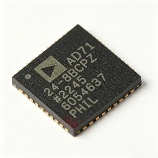
AD872ASD/883B - 12-Bit 10MSPS ADC | Analog Devices | Military
MPN: AD872ASD/883B ✓ Active| Qty | Unit Price | Extended |
|---|---|---|
| 1 | $786.32 | $786.32 |
| 10 | $750 | $7,500.00 |
| 100 | $700 | $70,000.00 |
| 500 | $650 | $325,000.00 |
| 1,000 | $600 | $600,000.00 |
AD872ASD/883B Overview
An analog-to-digital converter (ADC) is a device that converts continuous analog signals into discrete digital numbers, enabling digital processing of real-world signals. The AD872ASD/883B is a high-speed, 12-bit ADC that samples at 10 MSPS, making it suitable for applications requiring fast and accurate digitization, such as radar, electronic warfare, and high-speed data acquisition. It uses a proprietary BiCMOS architecture that balances speed and power consumption, and it includes an internal track-and-hold amplifier to maintain signal integrity during conversion.
Key features of the AD872ASD/883B include 12-bit resolution, a 10 MSPS sampling rate, and a parallel output interface. It operates from ±5V power supplies and features a proprietary method ADC architecture. The device is available in a 28-pin ceramic DIP, which provides excellent thermal performance and hermetic sealing for military and aerospace environments. The MIL-STD-883 Class B screening ensures compliance with stringent military quality standards.
Technically, the AD872ASD/883B integrates a track-and-hold amplifier and a voltage reference on-chip, reducing external component count and simplifying system design. The BiCMOS process technology enables high-speed operation while maintaining low power dissipation. The parallel word access output allows direct interface to digital signal processors (DSPs) and microcontrollers. The device is specified for operation from -55°C to +125°C, making it suitable for extreme temperature environments.
Typical applications include military radar systems, electronic warfare, high-speed data acquisition, and instrumentation. The AD872ASD/883B is also used in avionics and satellite communication systems where high reliability and wide temperature range are critical. Its 10 MSPS sampling rate and 12-bit resolution provide the performance needed for demanding signal processing tasks.
When designing with the AD872ASD/883B, ensure proper decoupling of the ±5V supplies and a clean analog ground plane to minimize noise. The internal reference simplifies design, but external reference can be used for improved accuracy. The parallel output should be buffered to avoid loading effects. Given its military-grade screening, the device is ideal for defense and aerospace applications where reliability is paramount.
Drop-in alternatives for AD872ASD/883B — same package, pin-to-pin compatible. Different-package parts requiring PCB rework are excluded.
Quick Comparison Tool — Select alternative parts for side-by-side comparison:
AD872ASD
✅ Drop-In📋 Reference alternative (not in catalog)
AD872AJD
✅ Drop-In📋 Reference alternative (not in catalog)
AD872AKD
✅ Drop-In ⚠️ Specs Unverified📋 Reference alternative (not in catalog)
AD872ATD
✅ Drop-In ⚠️ Specs Unverified📋 Reference alternative (not in catalog)
AD872AUD
✅ Drop-In ⚠️ Specs Unverified📋 Reference alternative (not in catalog)
AD872ASD/883B Maximum Ratings & Electrical Characteristics
| Resolution | 12 bits |
| Sampling Rate | 10 MSPS |
| Number of Channels | 1 |
| Input Type | Single-ended |
| Interface | Parallel |
| Architecture | Pipelined |
| Supply Voltage | ±5 V |
| Operating Temperature Range | -55°C to +125°C |
| Package | 28-pin CDIP |
| Mounting Type | Through-hole |
| Screening Level | MIL-STD-883 Class B |
| Technology | BiCMOS |
| RoHS Status | Non-compliant (military grade) |
| Number of Terminals | 28 |
| Package Code | DIP |
AD872ASD/883B Pin Configuration
| Pin 1 | VIN — Analog input |
| Pin 2 | VREF — Voltage reference input/output |
| Pin 3 | AGND — Analog ground |
| Pin 4 | AVDD — Positive analog supply (+5V) |
| Pin 5 | AVSS — Negative analog supply (-5V) |
| Pin 6 | CLK — Clock input |
| Pin 7 | OE — Output enable (active low) |
| Pin 8 | D0 — Digital output bit 0 (LSB) |
| Pin 9 | D1 — Digital output bit 1 |
| Pin 10 | D2 — Digital output bit 2 |
| Pin 11 | D3 — Digital output bit 3 |
| Pin 12 | D4 — Digital output bit 4 |
| Pin 13 | D5 — Digital output bit 5 |
| Pin 14 | D6 — Digital output bit 6 |
| Pin 15 | D7 — Digital output bit 7 |
| Pin 16 | D8 — Digital output bit 8 |
| Pin 17 | D9 — Digital output bit 9 |
| Pin 18 | D10 — Digital output bit 10 |
| Pin 19 | D11 — Digital output bit 11 (MSB) |
| Pin 20 | DGND — Digital ground |
| Pin 21 | DVDD — Digital supply (+5V) |
| Pin 22 | BUSY — Busy output (indicates conversion complete) |
| Pin 23 | NC — No connect |
| Pin 24 | NC — No connect |
| Pin 25 | NC — No connect |
| Pin 26 | NC — No connect |
| Pin 27 | NC — No connect |
| Pin 28 | NC — No connect |
Typical Applications
AD872ASD/883B is suitable for 6 applications: Military Radar Systems, Electronic Warfare, High-Speed Data Acquisition, Avionics, Satellite Communication, Instrumentation.
Military Radar Systems
The AD872ASD/883B is ideal for military radar systems due to its 12-bit resolution and 10 MSPS sampling rate, which enable accurate digitization of radar returns. Its MIL-STD-883 Class B screening ensures reliability in harsh environments, and the wide temperature range of -55°C to +125°C allows operation in extreme conditions. The on-chip track-and-hold amplifier maintains signal integrity, while the parallel interface simplifies connection to DSPs for real-time processing.
Recommended
Electronic Warfare
In electronic warfare systems, the AD872ASD/883B provides high-speed digitization of wideband signals. Its 10 MSPS sampling rate and 12-bit resolution capture fine details in signals, while the military temperature range and MIL-STD-883 screening ensure operation in demanding environments. The parallel output allows fast data transfer to FPGAs or DSPs for real-time analysis. The internal reference reduces external component count, simplifying system design.
Recommended
High-Speed Data Acquisition
The AD872ASD/883B is well-suited for high-speed data acquisition systems, offering 12-bit resolution at 10 MSPS. Its wide input bandwidth and on-chip track-and-hold amplifier ensure accurate sampling of fast transients. The device operates from ±5V supplies, making it compatible with common analog front-ends. The parallel interface enables straightforward connection to microcontrollers or DSPs. Its military-grade reliability makes it suitable for aerospace and defense data logging.
Recommended
Avionics
The AD872ASD/883B is used in avionics systems for flight control and navigation, where high reliability and wide temperature range are critical. Its 12-bit resolution and 10 MSPS sampling rate provide accurate digitization of sensor signals. The MIL-STD-883 Class B screening ensures compliance with military quality standards. The ceramic DIP package offers hermetic sealing, protecting against moisture and contaminants. The device operates over -55°C to +125°C, suitable for extreme flight conditions.
Recommended
Satellite Communication
In satellite communication systems, the AD872ASD/883B digitizes intermediate frequency (IF) signals for demodulation. Its 10 MSPS sampling rate and 12-bit resolution support high data rates, while the military temperature range ensures operation in space environments. The on-chip voltage reference reduces external components, saving board space. The parallel interface allows efficient data transfer to baseband processors. MIL-STD-883 screening provides confidence in long-term reliability.
Recommended
Instrumentation
The AD872ASD/883B is used in high-performance instrumentation, such as oscilloscopes and spectrum analyzers, where accurate digitization of signals is essential. Its 12-bit resolution and 10 MSPS sampling rate provide high dynamic range. The device's wide temperature range and military-grade screening make it suitable for field-deployed test equipment. The parallel output simplifies interface to display processors. The internal track-and-hold amplifier ensures accurate sampling of high-frequency signals.
Recommended
Recommended Products Summary
Engineering reference data for AD872ASD/883B — comparison, design guidance, and compliance information.
Selection Guide
Comparison with Alternatives
| Parameter | This Product | AD872ASD | AD872AJD | AD872AKD |
|---|---|---|---|---|
| Package | 28-pin CDIP | 28-pin CDIP | 28-pin CDIP | 28-pin CDIP |
| Brand | Analog Devices | Analog Devices | Analog Devices | Analog Devices |
| Resolution | 12 bits | 12 bits | 12 bits | 12 bits |
| Sampling Rate | 10 MSPS | 10 MSPS | 10 MSPS | 10 MSPS |
| Temperature Range | -55°C to +125°C | -55°C to +125°C | 0°C to +70°C | -40°C to +85°C |
| Screening | MIL-STD-883 Class B | None | None | None |
| Supply Voltage | ±5V | ±5V | ±5V | ±5V |
| Interface | Parallel | Parallel | Parallel | Parallel |
Key Differentiators
- MIL-STD-883 Class B screening (vs AD872ASD)
- Military temperature range (vs AD872AJD)
- Ceramic DIP package (vs AD872AJD)
Design Notes
The AD872ASD/883B requires ±5V supplies. Use low-noise linear regulators for analog and digital supplies to minimize noise coupling. Decouple each supply pin with 0.1µF ceramic capacitors placed close to the pins, and add 10µF tantalum capacitors for bulk decoupling. Ensure the analog and digital grounds are connected at a single point to avoid ground loops.
For optimal performance, use a multi-layer PCB with dedicated analog and digital ground planes. Keep the analog input traces short and shielded to reduce noise pickup. Place the ADC close to the signal source. Use a ground plane under the device to provide a low-impedance return path. Avoid routing digital signals near the analog input.
Ensure the clock input is clean and free of jitter, as it directly affects SNR. Use a low-jitter clock source. The analog input should be driven with a low-impedance source to avoid sampling errors. Do not exceed the absolute maximum ratings for supply voltages. The output enable pin (OE) should be tied low to enable outputs, or controlled for bus sharing.
Compliance Information
Military-grade component, not RoHS compliant due to lead-based solder and ceramic package. MIL-STD-883 screening.