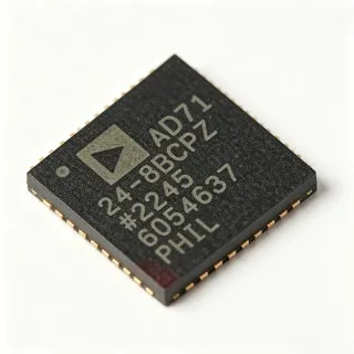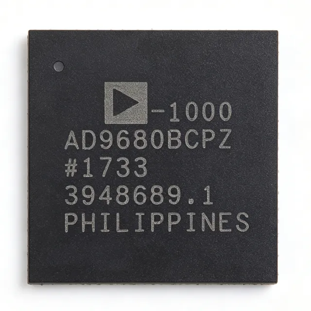
AD9680BCPZRL7-1000 - Dual 14-Bit 1 GSPS ADC JESD204B | Analog Devices
MPN: AD9680BCPZRL7-1000 ✓ Active| Qty | Unit Price | Extended |
|---|---|---|
| 1 | $0 | $0.00 |
| 10 | $0 | $0.00 |
| 100 | $0 | $0.00 |
| 500 | $0 | $0.00 |
| 1,000 | $0 | $0.00 |
AD9680BCPZRL7-1000 Overview
An analog-to-digital converter (ADC) is a mixed-signal semiconductor that samples a continuous analog waveform and quantizes it into discrete digital values. High-speed pipelined ADCs such as the AD9680 sit at the top of the data-converter hierarchy, bridging the analog front end of an RF or IF signal chain to a digital processor, FPGA, or ASIC. In modern wideband receivers, the ADC defines the system's instantaneous bandwidth, dynamic range, and noise floor, making its selection one of the most impactful decisions in a digital receiver design.
Key features of the AD9680 include dual 14-bit conversion cores rated at 1.25 GSPS (with the -1000 grade specified at 1 GSPS), an on-chip buffer and sample-and-hold circuit designed for low power, small size, and ease of use, and a JESD204B high-speed serial output that dramatically reduces pin count versus parallel LVDS/CMOS interfaces. The JESD204B lane interface supports multi-lane serialization with deterministic latency, simplifying FPGA interfacing.
Architecturally, the AD9680 uses a pipelined conversion architecture with on-chip references and buffering, which minimizes external analog component count. The device operates from 1.2 V and 2.5 V supplies per the datasheet title (1.2 V/2.5 V operation), supporting low overall power consumption for its class. Multiple sampling-rate grades (1.25 GSPS / 1 GSPS / 820 MSPS / 500 MSPS) share a common register map, and ADI's SPI Controller software supports the AD9680, AD9234, and AD9690, easing design migration within the family.
Typical applications include wideband software-defined radio (SDR) receivers, radar and electronic warfare digitizers, test and measurement instrumentation, and multi-channel communications infrastructure where two synchronized high-dynamic-range channels are required in a compact footprint.
Design considerations: the JESD204B link requires careful FPGA-side lane mapping and sysref timing design, and the exposed-pad LFCSP package demands a well-designed thermal via array under the pad for rated performance.
This page synthesizes distributor availability, same-family drop-in speed-grade alternatives, and practical design notes not found in the manufacturer datasheet alone. Pricing, where listed, is referenced as of 2026-09-05.
Drop-in alternatives for AD9680BCPZRL7-1000 — same package, pin-to-pin compatible. Different-package parts requiring PCB rework are excluded.
Quick Comparison Tool — Select alternative parts for side-by-side comparison:
AD9680BCPZ-1250
✓ In Stock
$840 / Unit
View Datasheet →AD9680BCPZ-500
✓ In Stock
Contact for price
View Datasheet →AD9680BCPZRL7-1250
📋 Reference alternative (not in catalog)
AD9234BCPZ-1250
📋 Reference alternative (not in catalog)
AD9690BCPZ-1250
📋 Reference alternative (not in catalog)
AD9680BCPZRL7-1000 Maximum Ratings & Electrical Characteristics
| Resolution | 14 bit |
| Number of Channels | 2 (dual) |
| Sampling Rate | 1 GSPS |
| Family Max Sampling Rate | 1.25 GSPS (device family; -1000 grade = 1 GSPS) |
| Architecture | Pipelined |
| Interface | JESD204B serial output |
| Supply Voltage | 1.2 V / 2.5 V |
| On-Chip Features | Buffer and sample-and-hold circuit |
| Package | 64-LFCSP (9 mm x 9 mm), exposed pad, HVQCCN |
| Mounting Type | Surface Mount |
| Terminal Form | No lead |
| Temperature Grade | Industrial |
| Packaging | Tape & Reel (RL7) |
AD9680BCPZRL7-1000 64-lfcsp (9 mm x 9 mm), exposed pad, hvqccn Pin Configuration Guide
Pin configuration for AD9680BCPZRL7-1000 (64-lfcsp (9 mm x 9 mm), exposed pad, hvqccn package). This analog component features input, output, and power supply pins. Refer to the manufacturer datasheet for offset null, compensation, and enable pin configurations. Ideal for signal conditioning and amplifier circuits.

No detailed pinout data available for AD9680BCPZRL7-1000.
Refer to the datasheet for full pin configuration.
Typical Applications
AD9680BCPZRL7-1000 is suitable for 6 applications: Wideband Software-Defined Radio, Radar and Electronic Warfare Digitizers, Test and Measurement Instrumentation, Communications Infrastructure Receivers, Multi-Channel Digital Beamforming, High-Energy Physics and Scientific Data Acquisition.
Wideband Software-Defined Radio
The AD9680BCPZRL7-1000's dual 14-bit, 1 GSPS sampling provides up to 500 MHz of instantaneous bandwidth per channel, which is the core requirement of modern wideband SDR receivers. Its JESD204B serial outputs connect directly to FPGA transceivers, eliminating wide parallel buses and simplifying board routing between the ADC and the digital baseband. The on-chip buffer and sample-and-hold reduce the drive requirements on the analog front end, allowing direct RF/IF sampling architectures with fewer gain stages. Because SDR platforms must cover multiple signal standards, the 1.2 V/2.5 V supply operation and ADI's shared SPI register map across the AD9680/AD9234/AD9690 family let designers scale resolution or speed without redesigning firmware.
Recommended
Radar and Electronic Warfare Digitizers
Radar and EW receivers demand both high dynamic range and wide bandwidth simultaneously; the dual 14-bit cores at 1 GSPS deliver the resolution needed to detect small targets near large clutter returns while digitizing hundreds of MHz of spectrum per channel. The 64-LFCSP 9 mm x 9 mm package supports compact multi-channel digitizer cards, and the industrial temperature grade suits defense platform environmental requirements. The JESD204B interface with deterministic latency ensures consistent sample-to-processing delay, which matters for pulse timing measurement. The ADI SPI Controller software shared across the AD9680/AD9234/AD9690 family accelerates bring-up in these programs.
Recommended
Test and Measurement Instrumentation
Oscilloscope front ends, spectrum analyzers, and arbitrary waveform receiver cards use dual GSPS ADCs to combine channels or implement interleaved sampling. The AD9680BCPZRL7-1000's 14-bit resolution preserves measurement fidelity for harmonics and spurious analysis, while 1 GSPS sampling covers wide capture windows. The on-chip buffer eases interfacing to high-bandwidth front-end amplifiers, and the JESD204B output keeps channel count and cable density manageable inside instruments. Since instrument platforms iterate across performance tiers, the shared register map with the -1250 and -500 grades allows one PCB to serve multiple instrument models with only a component change.
Recommended
Communications Infrastructure Receivers
Multi-carrier cellular and microwave backhaul receivers use direct-RF or wideband-IF sampling to digitize entire channel blocks. The dual channels of the AD9680BCPZRL7-1000 support diversity or MIMO paths in one device, halving the ADC count versus single-channel designs and improving channel-to-channel matching because both cores share the same reference and clocking. The 1.2 V/2.5 V supplies keep overall power competitive for dense baseband cards, and the 9 mm x 9 mm LFCSP suits high-density line-card layouts. JESD204B multi-lane output integrates cleanly with the FPGA pool that performs DDC and fronthaul functions.
Recommended
Multi-Channel Digital Beamforming
Phased-array radar and 5G massive-MIMO systems require many phase-coherent ADC channels; the AD9680BCPZRL7-1000 provides two matched 14-bit channels per device, and the JESD204B subclass supports deterministic latency alignment needed for coherent beam summation. Because all grades share the same die and pinout, a single beamformer PCB design can be populated with 500 MSPS, 1 GSPS, or 1.25 GSPS devices to trade bandwidth against power per application. The exposed-pad LFCSP with thermal via arrays supports the dense channel counts typical of array apertures, and ADI family-common SPI software simplifies calibration firmware across channel banks.
Recommended
High-Energy Physics and Scientific Data Acquisition
Particle detectors and laser-based scientific instruments need wideband, high-resolution waveform capture with tight channel synchronization. The dual 14-bit, 1 GSPS cores of the AD9680BCPZRL7-1000 capture fast analog pulses with sufficient resolution for charge and timing extraction, while JESD204B serialization keeps the digitizer-to-FPGA cabling manageable in large detector arrays. The industrial temperature grade tolerates non-lab environments, and the shared AD9680/AD9234/AD9690 register map lets research groups standardize one acquisition firmware stack across detector generations with differing resolution or speed requirements.
Recommended
Recommended Products Summary
Engineering reference data for AD9680BCPZRL7-1000 — comparison, design guidance, and compliance information.
Selection Guide
Comparison with Alternatives
| Parameter | This Product | AD9680BCPZ-1250 | AD9680BCPZ-500 | AD9234BCPZ-1250 | AD9690BCPZ-1250 |
|---|---|---|---|---|---|
| Package | 64-LFCSP (9x9) | 64-LFCSP (9x9) - same | 64-LFCSP (9x9) - same | 64-LFCSP (9x9) - same | 64-LFCSP (9x9) - same |
| Brand | Analog Devices | Analog Devices | Analog Devices | Analog Devices | Analog Devices |
| Resolution | 14 bit | 14 bit | 14 bit | 12 bit | 14 bit |
| Channel Count | 2 (dual) | 2 (dual) | 2 (dual) | 2 (dual) | 1 (single) |
| Output Interface | JESD204B | JESD204B | JESD204B | JESD204B | JESD204B |
| SPI Software Compatibility | Yes (AD9680/AD9234/AD9690 shared) | Yes (same register map) | Yes (same register map) | Yes (shared SPI Controller) | Yes (shared SPI Controller) |
Key Differentiators
- Full 1 GSPS sampling at 14-bit resolution (vs AD9234BCPZ-1250)
- Dual channels in one device (vs AD9690BCPZ-1250)
- Cost optimization potential via speed-grade pin compatibility (vs AD9680BCPZ-500)
Design Notes
The 64-LFCSP exposed pad is the primary ground and thermal path for the AD9680. Design the land pattern per the ADI datasheet with a central pad connected to a solid ground plane through a via array (typically 5x5 or denser, filled vias recommended). Do not route signals under the exposed pad region. Skimping on this pad connection degrades both thermal performance and analog ground integrity, which shows up directly as raised noise floor and spurs.
JESD204B operation requires a SYSREF signal distributed to both the ADC and the receiving FPGA with matched trace lengths and within the setup/hold timing window defined in the ADI datasheet. Serialize lane traces as 100-ohm differential pairs with intra-pair skew minimized and inter-lane skew managed per the datasheet lane alignment limits. Use ADI's SPI Controller software (shared with AD9234/AD9690) during bring-up to verify lane synchronization before system integration.
Do not mix speed grades casually: the AD9680BCPZ-500 is tested only to 500 MSPS and will not meet 1 GSPS dynamic-range specifications even though the die and footprint are identical. Similarly, the RL7 suffix indicates tape-and-reel packing - ordering the tray (non-RL7) variant breaks automated feeder setups. Confirm the exact supply sequencing and clock-jitter requirement (aperture jitter) from the official datasheet; clock phase noise directly limits SNR at 1 GSPS input frequencies.
Compliance Information
Verified web data for this MPN does not include formal compliance declarations. BC PZ package suffix conventionally indicates lead-free/RoHS production for ADI LFCSP parts, but official status must be confirmed via ADI product compliance documentation.