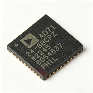
AD9751ASTZRL - 10-Bit 300 MSPS TxDAC+ DAC | Analog Devices
MPN: AD9751ASTZRL ✓ Active| Qty | Unit Price | Extended |
|---|---|---|
| 1 | $18.5 | $18.50 |
| 10 | $16.8 | $168.00 |
| 100 | $14.2 | $1,420.00 |
| 500 | $12.9 | $6,450.00 |
| 1,000 | $11.75 | $11,750.00 |
AD9751ASTZRL Overview
A digital-to-analog converter (DAC) is an electronic component that converts digital binary data into an analog voltage or current signal. DACs are essential in systems where digital processing must interface with the analog world, such as in transmitters, waveform generators, and audio equipment. The AD9751 belongs to the TxDAC+ family, which is optimized for high-speed, high-performance transmit paths in communication systems.
Key features of the AD9751 include excellent spurious-free dynamic range (SFDR) and intermodulation distortion (IMD) performance, with SFDR to Nyquist at 25 MHz output of 64 dB. It also features an internal clock doubling PLL, differential current outputs, and a flexible digital interface. The device operates from a single 3.3V supply and includes a power-down mode for reduced power consumption.
The AD9751 uses a segmented current-source architecture to achieve high linearity and low glitch energy. The dual muxed port architecture allows interleaving of data from two input ports, effectively doubling the data throughput. The internal PLL can double the input clock, simplifying system clocking. The device is specified over the industrial temperature range of -40°C to +85°C.
Typical applications include base stations, wireless local loop, digital radio links, direct digital synthesis (DDS), and arbitrary waveform generation. The high update rate and excellent dynamic performance make it ideal for generating complex modulated waveforms in communication transmitters.
When designing with the AD9751, careful attention to PCB layout is required to minimize parasitic capacitance and inductance, especially on the high-speed digital inputs and analog outputs. Proper decoupling of the analog and digital supplies is essential to achieve the specified dynamic performance.
Drop-in alternatives for AD9751ASTZRL — same package, pin-to-pin compatible. Different-package parts requiring PCB rework are excluded.
Variants in this series
Same-series models that are drop-in compatible with AD9751ASTZRL (same form factor and footprint) — differing in Output Type.
Quick Comparison Tool — Select alternative parts for side-by-side comparison:
AD9751ASTZ
✅ Drop-In✓ In Stock
$30.12 / Unit
View Datasheet →AD9751AST
✅ Drop-In📋 Reference alternative (not in catalog)
AD9751ASTZRL
✅ Drop-In✓ In Stock
$11.75 / Unit
View Datasheet →AD9746
⚡ Same Package ⚠️ Specs Unverified📋 Reference alternative (not in catalog)
DAC8565
⚡ Same Package ⚠️ Specs Unverified📋 Reference alternative (not in catalog)
LTC1660
⚡ Same Package ⚠️ Specs Unverified📋 Reference alternative (not in catalog)
AD9751ASTZRL Maximum Ratings & Electrical Characteristics
| Resolution | 10 Bit |
| Number of DAC Channels | 1 |
| Output Type | Current - Unbuffered |
| Differential Output | Yes |
| Data Interface | Parallel |
| Reference Type | External, Internal |
| Voltage - Supply, Analog | 3.3V |
| Voltage - Supply, Digital | 3.3V |
| Architecture | Segmented Current Source |
| Operating Temperature | -40°C ~ 85°C |
| Package / Case | 48-LQFP (7x7) |
| Mounting Type | Surface Mount |
| Packaging | Tape & Reel (TR) |
| SFDR to Nyquist @ 25 MHz Output | 64 dB |
| Output Update Rate | 300 MSPS |
| Internal Clock Doubling PLL | Yes |
AD9751ASTZRL Pin Configuration
| Pin 1 | CLK — Clock input |
| Pin 2 | GND — Ground |
| Pin 3 | DVDD — Digital supply |
| Pin 4 | D0 — Data input bit 0 |
| Pin 5 | D1 — Data input bit 1 |
| Pin 6 | D2 — Data input bit 2 |
| Pin 7 | D3 — Data input bit 3 |
| Pin 8 | D4 — Data input bit 4 |
| Pin 9 | D5 — Data input bit 5 |
| Pin 10 | D6 — Data input bit 6 |
| Pin 11 | D7 — Data input bit 7 |
| Pin 12 | D8 — Data input bit 8 |
| Pin 13 | D9 — Data input bit 9 |
| Pin 14 | MODE — Mode select |
| Pin 15 | PLL — PLL enable |
| Pin 16 | SLEEP — Power down |
| Pin 17 | AVDD — Analog supply |
| Pin 18 | IOUT — Current output |
| Pin 19 | IOUTB — Complementary current output |
| Pin 20 | COMP — Compensation |
| Pin 21 | REFIO — Reference input/output |
| Pin 22 | FSADJ — Full-scale adjust |
| Pin 23 | GND — Ground |
| Pin 24 | AVDD — Analog supply |
Typical Applications
AD9751ASTZRL is suitable for 6 applications: Base Station Transmitters, Direct Digital Synthesis (DDS), Arbitrary Waveform Generation, Digital Radio Links, Wireless Local Loop, Test and Measurement Equipment.
Base Station Transmitters
The AD9751ASTZRL is ideal for base station transmitters due to its 300 MSPS update rate and 64 dB SFDR, enabling generation of wideband modulated signals with high spectral purity. Its dual muxed port architecture allows interleaving of data to effectively double throughput, which is beneficial for multi-carrier applications. The internal PLL simplifies clocking, reducing system complexity. With a 3.3V supply, it integrates easily into modern base station designs. The industrial temperature range ensures reliable operation in outdoor environments.
Recommended
Direct Digital Synthesis (DDS)
The AD9751ASTZRL is well-suited for direct digital synthesis (DDS) systems, where its 300 MSPS update rate enables generation of high-frequency sine waves and complex waveforms. The excellent SFDR of 64 dB ensures low spurious content, critical for frequency-agile signal generation. The internal clock doubling PLL allows operation with lower frequency reference clocks, simplifying system design. The parallel interface supports high-speed data transfer from DSP or FPGA. This makes it ideal for test equipment, radar, and communication systems requiring precise waveform generation.
Recommended
Arbitrary Waveform Generation
The AD9751ASTZRL is excellent for arbitrary waveform generation (AWG) due to its high update rate and 10-bit resolution. It can produce complex waveforms with fine amplitude steps, suitable for testing and simulation. The dual muxed port architecture allows interleaving of data from two sources, enabling higher effective update rates. The differential current outputs can be converted to voltage using an external resistor or transformer, providing flexibility in output scaling. The industrial temperature range supports use in benchtop and field instruments.
Recommended
Digital Radio Links
The AD9751ASTZRL is designed for digital radio links, where high-speed DACs are required to generate IF signals for microwave transmitters. Its 300 MSPS update rate supports wideband modulation schemes, and the 64 dB SFDR ensures minimal spectral regrowth. The internal PLL simplifies clock generation, reducing component count. The 3.3V supply is compatible with modern digital logic. The compact 48-LQFP package is ideal for space-constrained radio modules. This makes it a reliable choice for point-to-point and point-to-multipoint radio systems.
Recommended
Wireless Local Loop
The AD9751ASTZRL is suitable for wireless local loop (WLL) systems, which require cost-effective, high-performance DACs for subscriber stations. Its 10-bit resolution and 300 MSPS update rate provide sufficient performance for voice and data transmission. The low power consumption of the 3.3V supply is beneficial for battery-powered or solar-powered installations. The industrial temperature range ensures operation in harsh outdoor environments. The dual muxed port architecture allows flexible data interleaving, simplifying interface to baseband processors.
Recommended
Test and Measurement Equipment
The AD9751ASTZRL is used in test and measurement equipment such as signal generators and arbitrary waveform generators. Its high update rate and excellent SFDR enable generation of clean, precise signals for testing. The parallel interface allows high-speed data streaming from FPGAs or DSPs. The internal PLL reduces external clock requirements. The industrial temperature range supports use in benchtop instruments. The compact package allows for dense PCB layouts, making it suitable for multi-channel instruments.
Recommended
Recommended Products Summary
Engineering reference data for AD9751ASTZRL — comparison, design guidance, and compliance information.
Selection Guide
Comparison with Alternatives
| Parameter | This Product | AD9751ASTZ | AD9751AST | AD9746 | DAC8565 | LTC1660 |
|---|---|---|---|---|---|---|
| Package | 48-LQFP (7x7) | 48-LQFP (7x7) | 48-LQFP (7x7) | 48-LQFP (7x7) | 48-LQFP (7x7) | 48-LQFP (7x7) |
| Brand | Analog Devices | Analog Devices | Analog Devices | Analog Devices | Texas Instruments | Analog Devices |
| Resolution | 10 Bit | 10 Bit | 10 Bit | 14 Bit | 16 Bit | 16 Bit |
| Data Interface | Parallel | Parallel | Parallel | Parallel | SPI | SPI |
| Supply Voltage | 3.3V | 3.3V | 3.3V | 3.3V | 2.7V to 5.5V | 2.7V to 5.5V |
| Operating Temperature | -40°C to +85°C | -40°C to +85°C | -40°C to +85°C | -40°C to +85°C | -40°C to +105°C | -40°C to +85°C |
Key Differentiators
- 300 MSPS update rate with 10-bit resolution (vs AD9746 (14-bit))
- Internal clock doubling PLL (vs DAC8565 (16-bit))
- Dual muxed port architecture (vs LTC1660 (16-bit))
Design Notes
For optimal performance, place decoupling capacitors (0.1uF and 10uF) close to each supply pin (AVDD, DVDD). Use a solid ground plane and separate analog and digital ground planes, connecting them at a single point near the device. Keep high-speed digital traces short and matched in length to minimize skew. The differential current outputs (IOUT, IOUTB) should be routed as a controlled impedance pair to the load or transformer.
The AD9751ASTZRL operates from a 3.3V supply. Ensure the supply is clean and well-regulated, as noise on the supply can degrade SFDR. Use a low-dropout regulator (LDO) to provide a stable 3.3V rail, and add ferrite beads to isolate analog and digital supplies. The total current consumption is typically [DATA_NEEDED: supply current], so size the regulator accordingly.
The AD9751ASTZRL in a 48-LQFP package has a thermal resistance (theta_JA) of approximately [DATA_NEEDED: theta_JA]. Power dissipation is typically low for a DAC, but ensure adequate copper area on the PCB for heat spreading. For high ambient temperatures, consider adding thermal vias under the exposed pad (if present) to improve heat transfer to the ground plane.
Compliance Information
The 'Z' suffix indicates lead-free (RoHS compliant) finish. Other compliance details not specified in the provided data.