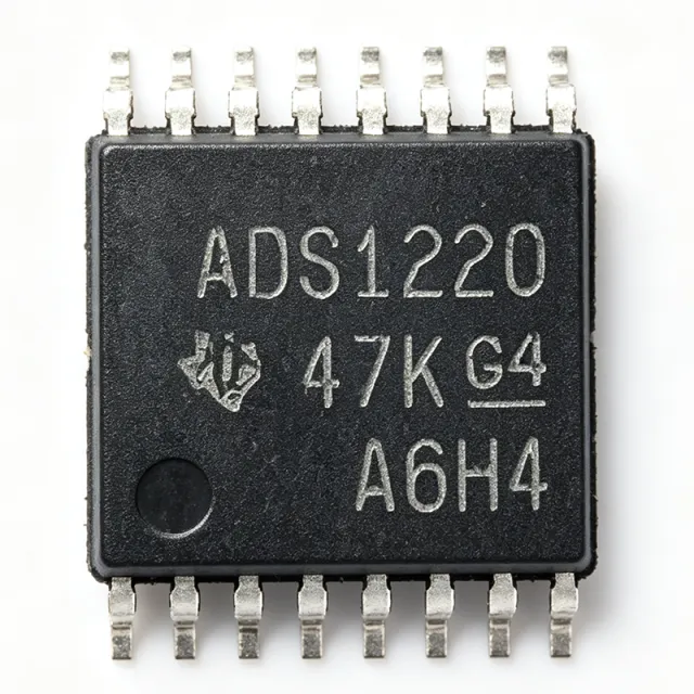
ADS1220IPWR - 24-Bit 2kSPS Delta-Sigma ADC | Texas Instruments
MPN: ADS1220IPWR ✓ Active| Qty | Unit Price | Extended |
|---|---|---|
| 1 | $2.65 | $2.65 |
| 10 | $2.35 | $23.50 |
| 100 | $2.1 | $210.00 |
| 500 | $1.98 | $990.00 |
| 1,000 | $1.91 | $1,910.00 |
ADS1220IPWR Overview
A delta-sigma ADC is a type of analog-to-digital converter that oversamples the input signal and applies digital filtering to achieve very high resolution, making it the dominant architecture in the precision data-converter hierarchy (ADC -> precision ADC -> sigma-delta ADC -> data converter) for measuring small sensor signals. Where successive-approximation (SAR) ADCs favor speed, delta-sigma converters favor noise-free resolution, which is why they dominate sensor front ends.
Key features of the ADS1220 include a flexible input multiplexer supporting two differential or four single-ended inputs, a low-noise PGA that reduces system component count, two integrated matched IDACs for ratiometric 3-wire and 4-wire RTD measurements, and an on-chip reference that eliminates external reference circuitry. The integration of PGA, VREF and IDACs in a small TSSOP-16 footprint is the part's central value proposition: TI positions it explicitly as a way to reduce system cost and bill-of-materials count in small-signal sensor applications.
Architecturally, the device combines the delta-sigma modulator with a programmable digital filter, allowing trade-offs between output data rate (up to 2 kSPS) and noise performance. The SPI-compatible serial interface provides data reads, register configuration, and a DRDY output for deterministic cycle timing, simplifying interfacing with any MCU, including TI MSP430 and other low-power hosts.
Typical applications include RTD and thermocouple temperature measurement, bridge sensors such as load cells and pressure sensors, battery monitoring, and portable industrial instrumentation where low power and small size matter.
Design consideration: use the two IDACs with a precision reference resistor to build ratiometric RTD front ends; this cancels IDAC drift from the measurement, but budget the PGA headroom so IDAC compliance voltage plus sensor drop stays within the supply.
This page synthesizes distributor pricing, drop-in alternatives, pinout, design notes and comparison data not consolidated in the manufacturer datasheet.
Drop-in alternatives for ADS1220IPWR — same package, pin-to-pin compatible. Different-package parts requiring PCB rework are excluded.
Variants in this series
Same-series models that are drop-in compatible with ADS1220IPWR (same form factor and footprint) — differing in Package, Architecture, Resolution, 50/60 Hz Rejection, Converter Type.
Quick Comparison Tool — Select alternative parts for side-by-side comparison:
MCT1220
📋 Reference alternative (not in catalog)
ADS1220IPWR Maximum Ratings & Electrical Characteristics
| Resolution | 24 bit |
| Maximum Sample Rate | 2 kSPS |
| Input Channels | 4 (2 differential or 4 single-ended) |
| Architecture | Sigma-Delta |
| Interface | SPI |
| Integrated PGA | Yes, low-noise programmable gain amplifier |
| Integrated Reference | Yes, internal VREF |
| Excitation Current Sources | 2 programmable IDACs |
| Package | 16-TSSOP |
| Operating Temperature | -40C to +125C |
| Mounting Type | Surface Mount |
| Power Consumption | Low power (per TI product description) |
| Typical Price (qty 1) | from $1.91 (LCSC, as of 2026-09-03) |
ADS1220IPWR Pin Configuration
| Pin 1 | AIN0 — Analog input 0 / multiplexer input |
| Pin 2 | AIN1 — Analog input 1 / multiplexer input |
| Pin 3 | AIN2 — Analog input 2 / multiplexer input |
| Pin 4 | AIN3 — Analog input 3 / multiplexer input |
| Pin 5 | AVSS — Analog negative supply / ground |
| Pin 6 | AVDD — Analog positive supply |
| Pin 7 | DOUT/DRDY — Serial data output / data-ready indicator |
| Pin 8 | SCLK — SPI serial clock input |
| Pin 9 | DIN — SPI serial data input |
| Pin 10 | CS — SPI chip select (active low) |
| Pin 11 | DVDD — Digital supply |
| Pin 12 | DGND — Digital ground |
| Pin 13 | REFN0 — External reference 0 negative input |
| Pin 14 | REFP0 — External reference 0 positive input |
| Pin 15 | REFP1/AIN0 — Alternate reference 0 positive input / multiplexed analog input (per datasheet) |
| Pin 16 | REFN1/AIN1 — Alternate reference 0 negative input / multiplexed analog input (per datasheet) |
Typical Applications
ADS1220IPWR is suitable for 6 applications: RTD Temperature Measurement, Thermocouple Input Modules, Load Cell and Bridge Sensor Weighing, Battery-Powered Portable Instrumentation, Pressure Sensor Signal Conditioning, Battery Management and Cell Monitoring.
RTD Temperature Measurement
The ADS1220IPWR fits RTD measurement because its two programmable IDACs, integrated PGA and on-chip reference form a complete ratiometric front end: the IDACs excite the RTD, the PGA amplifies millivolt-level signals into the 24-bit ADC range, and the matched current sources enable 3-wire and 4-wire lead-resistance cancellation. In a typical PT100 circuit the IDAC current is routed through the sensor and a precision reference resistor, so the ADC digitizes the ratio and IDAC drift largely cancels. At slow data rates the noise floor supports sub-0.1C resolution, and the low-power operation suits multi-channel temperature banks polled sequentially through the input multiplexer.
Recommended
Thermocouple Input Modules
Thermocouples produce microvolt-per-degree signals, which is precisely where the ADS1220IPWR's 24-bit delta-sigma core and low-noise PGA deliver value: at low data rates the effective resolution resolves tens of microvolts, enough for fraction-of-a-degree accuracy across type K, J and T elements. Cold-junction compensation is handled by routing an RTD or on-board sensor to a spare multiplexer channel, all digitized by the same IC. The integrated reference removes one external precision component, and the SPI interface plus DRDY output lets a low-cost MCU cycle-read multiple thermocouple channels deterministically. Industrial thermocouple input modules therefore collapse an entire analog front end into one small TSSOP-16 device.
Recommended
Load Cell and Bridge Sensor Weighing
Strain-gauge load cells output only a few millivolts per volt of excitation, so bridge measurement demands high resolution and clean gain - both strengths of the ADS1220IPWR. The PGA boosts the differential bridge signal to exploit the full 24-bit dynamic range, while the internal reference supports ratiometric operation that cancels excitation-voltage drift from the weight reading. At 2 kSPS maximum rate the device covers typical weigh-scale and force-sensing update requirements, and its low power suits battery-powered portable scales. The small 16-TSSOP footprint lets designers embed the front end close to the load cell connector, shortening analog traces and improving noise immunity in industrial weighing systems.
Recommended
Battery-Powered Portable Instrumentation
The ADS1220IPWR's low-power delta-sigma architecture, duty-cycled operation through its SPI interface, and integration of PGA, reference and IDACs make it attractive for battery-powered data loggers and handheld meters. Because one IC replaces a PGA, reference and current-source BOM section, quiescent budget and board area both shrink - key constraints in portable devices. The multiplexer allows one ADS1220 to scan several sensors sequentially under MCU control, further reducing per-channel power. Designers typically keep the converter in shutdown between conversions and exploit DRDY interrupt timing so the host MCU sleeps during conversions, extending battery life in field instrumentation measuring pressure, temperature or pH.
Recommended
Pressure Sensor Signal Conditioning
Bridge-type pressure transducers, like load cells, produce small differential outputs that the ADS1220IPWR digitizes directly: the PGA provides the gain, the delta-sigma core supplies 24-bit resolution, and ratiometric reference operation ties the reading to the excitation source so supply drift cancels. In industrial pressure transmitters the IDACs can also support diagnostics by injecting test currents through the bridge to detect open or shorted elements - a common functional-safety requirement. The device's -40C to +125C rating covers most process-instrument ambient ranges, and its compact TSSOP-16 package fits the tight headspace of transmitter housings, making the ADS1220 a frequent front-end choice in pressure module designs.
Recommended
Battery Management and Cell Monitoring
While dedicated battery-management ICs handle stack supervision, the ADS1220IPWR serves precision auxiliary measurement in BMS front ends: monitoring shunt or hall-derived current signals, sense-resistor voltages, and temperature arrays with 24-bit accuracy. The PGA handles small shunt voltages directly, and the IDACs can excite NTC thermistor dividers for temperature readings referenced to the same internal reference, keeping all channels consistent. Where eight simultaneous channels are needed, TI's ADS131M08 complements rather than replaces the ADS1220; the latter excels when a few high-accuracy, low-rate channels must be measured inside a power-constrained pack-level board. The -40C to +125C range matches automotive-adjacent battery environments.
Recommended
Recommended Products Summary
Engineering reference data for ADS1220IPWR — comparison, design guidance, and compliance information.
Selection Guide
Comparison with Alternatives
| Parameter | This Product | MCT1220 |
|---|---|---|
| Package | 16-TSSOP | 16-TSSOP - same |
| Brand | Texas Instruments | Nanjing Modu Zhixin |
| Resolution | 24 bit | 24 bit |
| Input Channels | 4 (2 diff / 4 SE) | 4 (2 diff / 4 SE) |
| Integrated PGA | Yes | Yes |
| IDACs | 2 programmable | 2 programmable |
| Interface | SPI | SPI |
Key Differentiators
- Complete analog front-end integration (vs MCT1220)
- Two matched IDACs purpose-built for RTD wiring cancellation (vs ADS1256)
- Trade-off: 2 kSPS ceiling (vs ADS1256)
Design Notes
Separate the analog and digital ground domains and join them at a single star point beneath the ADS1220IPWR. Place the AVDD and DVDD decoupling capacitors (typ. 100 nF ceramic plus bulk) within 2 mm of pins 6/11 respectively, with solid return paths. Keep the switched SPI lines (SCLK, DIN) away from AIN0-AIN3 and REFP0/REFN0 traces to prevent digital noise coupling into the 24-bit measurement path. Use a ground pour under the ADC region and route the reference-input traces as short, matched pairs.
Because the ADS1220 is a delta-sigma converter, the digital filter attenuates out-of-band noise but the front end is still sensitive to differential-mode and common-mode interference at low data rates. Use RC differential and common-mode filtering on the analog inputs (antialiasing and EMI), and when using external REFP0/REFN0, drive the reference from a low-noise source or use the internal reference. Apply ratiometric configurations (reference resistor + IDAC) wherever possible so drift terms cancel instead of being specified out.
Verify PGA input headroom when IDACs are active: excitation current through the sensor plus reference resistor must stay inside the PGA linear range at the chosen gain, or the reading will clip silently. Also remember CS must frame every SPI transaction and DRDY (shared on DOUT) must be monitored to read complete conversions - reading mid-conversion returns stale data. When converting a design from the ADS1220 TSSOP-16 to the VQFN-16 variant, the footprint is NOT drop-in; pads differ.
Compliance Information
Standard current-production TI catalog part in lead-free TSSOP; formal RoHS/REACH declarations should be pulled from TI's quality portal for your date code.