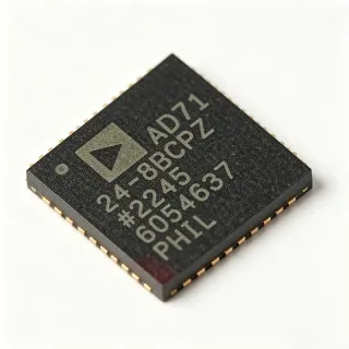
ADV7391BCPZ-RL - 10-Bit SD/HD Video Encoder | Analog Devices
MPN: ADV7391BCPZ-RL ✗ End of Life| Qty | Unit Price | Extended |
|---|---|---|
| 1 | $6.77 | $6.77 |
| 10 | $6.23 | $62.30 |
| 100 | $5.42 | $542.00 |
| 500 | $4.88 | $2,440.00 |
| 1,000 | $4.39 | $4,390.00 |
ADV7391BCPZ-RL Overview
A video encoder is an integrated circuit that converts digital video data into analog video signals for display or transmission. In the signal chain, the video encoder sits between a digital video source (such as a video processor, FPGA, or SoC) and the analog display interface (such as composite, S-Video, or component outputs). The ADV7391 belongs to the family of digital-to-analog video encoders, which are essential in applications ranging from consumer TVs to professional video equipment. Its role is to bridge the digital and analog domains, ensuring high-quality video output with minimal artifacts.
Key features of the ADV7391BCPZ-RL include support for both standard-definition (SD) and high-definition (HD) video formats, with a maximum DAC sampling rate of 297 Msps. The device provides three 10-bit DACs, enabling simultaneous output of CVBS, S-Video, and component signals. It also includes an on-chip voltage reference and supports both interlaced and progressive scan formats. The low power consumption of 81 mA at 3.3 V makes it an excellent choice for battery-powered devices, while the wide operating temperature range of -40°C to +85°C ensures reliability in industrial environments.
From a technical perspective, the ADV7391 utilizes a high-speed digital-to-analog conversion architecture that ensures accurate color reproduction and sharp image detail. The device features a flexible digital interface that supports both 4:2:2 and 4:4:4 YCrCb data formats, as well as embedded synchronization signals. The on-chip PLL allows for precise clock generation, reducing external component count. The ADV7391 is part of a family that includes the ADV7390, ADV7392, and ADV7393, which offer different feature sets and package options, allowing designers to select the optimal part for their specific application.
Typical applications for the ADV7391BCPZ-RL include set-top boxes, DVD/Blu-ray players, video game consoles, and digital signage. Its low power consumption and small footprint make it ideal for portable media players and handheld devices. The device is also suitable for automotive infotainment systems, where its wide temperature range and robust performance are critical.
When designing with the ADV7391BCPZ-RL, it is important to ensure proper decoupling of the power supply pins and to route the analog video outputs away from digital noise sources. The device requires an external crystal or clock source, and the PCB layout should minimize parasitic capacitance on the DAC outputs to maintain signal integrity.
Drop-in alternatives for ADV7391BCPZ-RL — same package, pin-to-pin compatible. Different-package parts requiring PCB rework are excluded.
Variants in this series
Same-series models that are drop-in compatible with ADV7391BCPZ-RL (same form factor and footprint) — differing in Lifecycle Status, Package, Supply Current.
Quick Comparison Tool — Select alternative parts for side-by-side comparison:
ADV7391BCPZ
✅ Drop-In✓ In Stock
$6.5 / Unit
View Datasheet →ADV7391BCPZ-REEL
✅ Drop-In📋 Reference alternative (not in catalog)
ADV7392BCPZ
✅ Drop-In ⚠️ Specs Unverified📋 Reference alternative (not in catalog)
ADV7393BCPZ
✅ Drop-In ⚠️ Specs Unverified📋 Reference alternative (not in catalog)
ADV7390BCPZ
✅ Drop-In ⚠️ Specs Unverified📋 Reference alternative (not in catalog)
ADV7391BCPZ-RL Specifications
| Function | Video Encoder |
| Resolution | 10-bit |
| Number of DACs | 3 |
| DAC Sampling Rate | 297 Msps |
| Supply Voltage | 1.71 V to 3.63 V |
| Supply Current | 81 mA |
| Operating Temperature Range | -40°C to +85°C |
| Package | 32-LFCSP-VQ (5x5 mm) |
| Mounting Type | Surface Mount |
| Video Output Formats | CVBS, S-Video, YPrPb |
| Digital Interface | 4:2:2 and 4:4:4 YCrCb |
| On-Chip PLL | Yes |
| On-Chip Voltage Reference | Yes |
| Lifecycle Status | Not Recommended for New Designs |
| RoHS Status | Compliant |
ADV7391BCPZ-RL Pin Configuration
| Pin 1 | DVDD — Digital power supply |
| Pin 2 | DGND — Digital ground |
| Pin 3 | P0 — Digital video input bit 0 |
| Pin 4 | P1 — Digital video input bit 1 |
| Pin 5 | P2 — Digital video input bit 2 |
| Pin 6 | P3 — Digital video input bit 3 |
| Pin 7 | P4 — Digital video input bit 4 |
| Pin 8 | P5 — Digital video input bit 5 |
| Pin 9 | P6 — Digital video input bit 6 |
| Pin 10 | P7 — Digital video input bit 7 |
| Pin 11 | P8 — Digital video input bit 8 |
| Pin 12 | P9 — Digital video input bit 9 |
| Pin 13 | CLKIN — Clock input |
| Pin 14 | AVDD — Analog power supply |
| Pin 15 | AGND — Analog ground |
| Pin 16 | COMP — Compensation pin |
| Pin 17 | CVBS — Composite video output |
| Pin 18 | Y — Luminance output |
| Pin 19 | C — Chrominance output |
| Pin 20 | Pr — Component Pr output |
| Pin 21 | Pb — Component Pb output |
| Pin 22 | AGND — Analog ground |
| Pin 23 | AVDD — Analog power supply |
| Pin 24 | I2C_SDA — I2C data |
| Pin 25 | I2C_SCL — I2C clock |
| Pin 26 | RESET — Reset input |
| Pin 27 | PWRDN — Power down input |
| Pin 28 | DVDD — Digital power supply |
| Pin 29 | DGND — Digital ground |
| Pin 30 | XTAL_IN — Crystal oscillator input |
| Pin 31 | XTAL_OUT — Crystal oscillator output |
| Pin 32 | EP — Exposed pad (ground) |
Typical Applications
ADV7391BCPZ-RL is suitable for 6 applications: Set-Top Boxes, Video Players, Digital Signage, Portable Media Players, Automotive Infotainment, Video Game Consoles.
Set-Top Boxes
The ADV7391BCPZ-RL provides high-quality analog video output for set-top boxes, converting digital video streams to CVBS, S-Video, or component signals. Its low power consumption (81 mA) and small 5x5 mm package make it ideal for space-constrained designs. The 10-bit DACs ensure accurate color reproduction, essential for consumer video quality. With support for both SD and HD formats, it can handle various broadcast standards. The device's wide operating temperature range (-40°C to +85°C) ensures reliable operation in home environments. Designers can easily interface it with SoCs or FPGAs via the digital video input port.
Recommended
Video Players
In DVD and Blu-ray players, the ADV7391BCPZ-RL converts digital video data into analog signals for TV output. Its three DACs support simultaneous CVBS and component outputs, allowing connection to both composite and component inputs. The 297 Msps DAC sampling rate ensures sharp HD images. Low power consumption extends device lifespan and reduces heat. The on-chip PLL simplifies clock generation, reducing external components. The compact LFCSP package fits slim player designs. The device's robust performance ensures consistent video quality across different media formats.
Recommended
Digital Signage
The ADV7391BCPZ-RL is well-suited for digital signage, where reliable video output is critical. It supports HD formats up to 297 Msps, ensuring crisp images on large displays. The low power consumption (81 mA) reduces heat in enclosed signage systems. The wide temperature range (-40°C to +85°C) allows outdoor installation. The device's small package enables compact media players. With multiple output formats (CVBS, S-Video, YPrPb), it can drive various display types. The on-chip voltage reference reduces external component count, simplifying design.
Recommended
Portable Media Players
For portable media players, the ADV7391BCPZ-RL offers low power consumption (81 mA) and a compact 5x5 mm package, ideal for battery-powered devices. It supports both SD and HD video output, allowing connection to TVs or monitors. The 10-bit DACs provide high-quality video with minimal artifacts. The device operates from 1.71 V to 3.63 V, compatible with common battery voltages. The wide temperature range ensures operation in various environments. The on-chip PLL reduces external components, saving board space. This makes it an excellent choice for handheld video devices.
Recommended
Automotive Infotainment
The ADV7391BCPZ-RL is suitable for automotive infotainment systems, providing analog video output for rear-seat displays and head units. Its wide operating temperature range (-40°C to +85°C) meets automotive requirements. The low power consumption reduces heat in the dashboard. The device supports multiple video formats, enabling connection to various display types. The compact package fits space-constrained automotive electronics. The 10-bit DACs ensure clear video for navigation and entertainment. The on-chip PLL simplifies clock generation, reducing EMI. This makes it a reliable choice for in-vehicle video applications.
Recommended
Video Game Consoles
In video game consoles, the ADV7391BCPZ-RL converts digital game graphics to analog video for TV output. Its high DAC sampling rate (297 Msps) supports HD gaming. The three DACs allow simultaneous composite and component output, accommodating various TV inputs. Low power consumption reduces heat in the console. The compact package fits internal PCB space. The device's robust performance ensures smooth video with minimal lag. The on-chip PLL reduces external components, simplifying design. This makes it an ideal choice for gaming systems.
Recommended
Recommended Products Summary
Engineering reference data for ADV7391BCPZ-RL — comparison, design guidance, and compliance information.
Selection Guide
Comparison with Alternatives
| Parameter | This Product | ADV7391BCPZ | ADV7391BCPZ-REEL | ADV7392BCPZ | ADV7393BCPZ | ADV7390BCPZ |
|---|---|---|---|---|---|---|
| Package | 32-LFCSP-VQ (5x5 mm) | 32-LFCSP-VQ (5x5 mm) - same | 32-LFCSP-VQ (5x5 mm) - same | 32-LFCSP-VQ (5x5 mm) - same | 32-LFCSP-VQ (5x5 mm) - same | 32-LFCSP-VQ (5x5 mm) - same |
| Brand | Analog Devices | Analog Devices | Analog Devices | Analog Devices | Analog Devices | Analog Devices |
| Resolution | 10-bit | 10-bit | 10-bit | 10-bit | 10-bit | 10-bit |
| Number of DACs | 3 | 3 | 3 | 3 | 3 | 3 |
| DAC Sampling Rate | 297 Msps | 297 Msps | 297 Msps | 297 Msps | 297 Msps | 216 Msps |
| Supply Voltage | 1.71 V to 3.63 V | 1.71 V to 3.63 V | 1.71 V to 3.63 V | 1.71 V to 3.63 V | 1.71 V to 3.63 V | 1.71 V to 3.63 V |
| Supply Current | 81 mA | 81 mA | 81 mA | 85 mA | 88 mA | 75 mA |
| Video Output Formats | CVBS, S-Video, YPrPb | CVBS, S-Video, YPrPb | CVBS, S-Video, YPrPb | CVBS, S-Video, YPrPb | CVBS, S-Video, YPrPb | CVBS, S-Video, YPrPb |
Key Differentiators
- Low power consumption of 81 mA (vs ADV7392BCPZ)
- Supports HD formats up to 297 Msps (vs ADV7390BCPZ)
- Tape and reel packaging for automated assembly (vs ADV7391BCPZ)
Design Notes
The ADV7391BCPZ-RL operates from 1.71 V to 3.63 V, with separate analog (AVDD) and digital (DVDD) supplies. Use low-impedance decoupling capacitors (0.1 uF and 10 uF) close to each supply pin to minimize noise. The device draws 81 mA typical, so ensure the power supply can handle peak currents during video output transitions.
Route analog video outputs (CVBS, Y, C, Pr, Pb) away from digital signals to prevent noise coupling. Use ground planes to provide a low-impedance return path. Keep the exposed pad (EP) connected to a solid ground plane for thermal and electrical performance. Minimize parasitic capacitance on DAC outputs to maintain signal integrity.
Ensure proper crystal or clock source is connected to XTAL_IN and XTAL_OUT. The device requires an external clock for operation. Do not leave the RESET pin floating; tie it high or use a pull-up resistor. The PWRDN pin should be controlled to enter low-power mode when needed. Verify I2C address configuration to avoid conflicts.
Compliance Information
RoHS compliant per Analog Devices product page. AEC-Q100 not applicable for this consumer/industrial part.