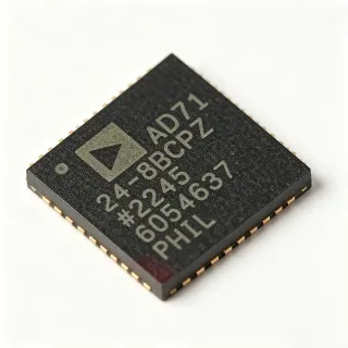
DG412 - Quad SPST CMOS Analog Switch 44V | Analog Devices
MPN: DG412 ✓ Active| Qty | Unit Price | Extended |
|---|---|---|
| 1 | $4.18 | $4.18 |
| 10 | $3.76 | $37.60 |
| 100 | $3.34 | $334.00 |
| 500 | $3.05 | $1,525.00 |
| 1,000 | $2.85 | $2,850.00 |
DG412 Overview
An analog switch is a semiconductor device that passes or blocks an analog signal under digital control, acting as a relay replacement without moving parts. Within the signal-path hierarchy, the analog switch sits under signal switching ICs, itself a branch of interface and signal-conditioning semiconductors. Quad SPST devices such as the DG412 integrate four independent switches on one die, letting one logic-controlled part replace four discrete transistor-level switching circuits while preserving signal integrity.
Key features include TTL- and CMOS-compatible logic inputs, fast switching with turn-on time around 110 ns per the original datasheet family, ultra-low power dissipation near 0.35 mW quiescent, and improved on-resistance matching between switches of 3 ohm max with guaranteed rDS(on) flatness over the signal range of 4 ohm max in the redesigned Maxim version. The wide 44 V absolute maximum supply rating supports +/-15 V industrial analog rails.
Architecturally, the DG412 family uses monolithic CMOS transmission-gate switches with internal level shifting, allowing a single 5 V logic signal to control signals swinging to +/-15 V. Drop-in compatibility with the older DG211/DG212 series simplifies legacy redesigns.
Typical applications include audio signal routing, precision test-and-measurement multiplexing, data-acquisition front ends, sample-and-hold circuits, and industrial signal switching where relay-free switching is required.
Design consideration: keep control-input logic levels within datasheet limits and observe the analog signal range so switches never see signals beyond the supply rails, which would turn on protection structures and distort the signal.
This page synthesizes distributor pricing, verified drop-in alternatives from Analog Devices, Renesas and Vishay, and practical design notes not found in the manufacturer datasheet.
Drop-in alternatives for DG412 — same package, pin-to-pin compatible. Different-package parts requiring PCB rework are excluded.
Variants in this series
Same-series models that are drop-in compatible with DG412 (same form factor and footprint) — differing in Package, Switch Configuration, Analog Signal Range, On-Resistance (rDS on), Power Dissipation.
Quick Comparison Tool — Select alternative parts for side-by-side comparison:
DG412DY+
✅ Drop-In📋 Reference alternative (not in catalog)
DG411DY+
✅ Drop-In📋 Reference alternative (not in catalog)
DG413DY+
✅ Drop-In📋 Reference alternative (not in catalog)
DG412DYZ
✅ Drop-In📋 Reference alternative (not in catalog)
DG412DY-E3
✅ Drop-In📋 Reference alternative (not in catalog)
DG412 Maximum Ratings & Electrical Characteristics
| Function | Quad SPST Analog Switch (4 x NO) |
| Switch Configuration | 4 independent 1:1 SPST |
| On-Resistance (rDS on) | 45 ohm max (ADI/Maxim); 35 ohm (Vishay/Renesas grade) |
| On-Resistance Matching | 3 ohm max (redesigned Maxim version) |
| On-Resistance Flatness | 4 ohm max over signal range |
| Turn-On Time (tON) | 110 ns (typ., family datasheet) |
| Analog Signal Range | +/-15 V |
| Maximum Supply Rating | 44 V |
| Logic Inputs | TTL and CMOS compatible |
| Power Dissipation | 0.35 mW (ultra low, quiescent) |
| Supply Type | Dual supply supported; single supply capable |
| Package | SOIC-16 (16-SOIC) |
| Mounting Type | Surface Mount |
| Drop-in Compatibility | Replaces DG211/DG212 series |
DG412 Pin Configuration
| Pin 1 | IN1 — Logic control input, switch 1 (TTL/CMOS compatible) |
| Pin 2 | IN2 — Logic control input, switch 2 |
| Pin 3 | IN3 — Logic control input, switch 3 |
| Pin 4 | IN4 — Logic control input, switch 4 |
| Pin 5 | V- — Negative supply |
| Pin 6 | GND — Ground |
| Pin 7 | NC — Not connected (per datasheet) |
| Pin 8 | NC — Not connected (per datasheet) |
| Pin 9 | NO1 — Switch 1, normally-open terminal |
| Pin 10 | COM1 — Switch 1, common terminal |
| Pin 11 | NO2 — Switch 2, normally-open terminal |
| Pin 12 | COM2 — Switch 2, common terminal |
| Pin 13 | NO3 — Switch 3, normally-open terminal |
| Pin 14 | COM3 — Switch 3, common terminal |
| Pin 15 | NO4 — Switch 4, normally-open terminal |
| Pin 16 | COM4 — Switch 4, common terminal |
Typical Applications
DG412 is suitable for 6 applications: Audio Signal Routing, Data Acquisition Front Ends, Test and Measurement Multiplexing, Industrial Signal Switching (44V Rails), Sample-and-Hold and Integrator Circuits, Legacy DG211/DG212 Board Upgrades.
Audio Signal Routing
The DG412 fits audio routing matrices because its CMOS transmission-gate construction switches line-level signals without relay wear or contact bounce, and the redesigned ADI version guarantees 3 ohm max on-resistance matching between the four switches with 4 ohm max flatness, preserving channel-to-channel gain consistency. With a +/-15 V analog signal range, it passes professional balanced and unbalanced line levels with ample headroom. Each switch is placed directly in the signal path ahead of buffers or summing amps, controlled by TTL/CMOS logic from a microcontroller. Unlike relays, it draws only about 0.35 mW quiescent power and switches in roughly 110 ns, enabling silent, click-free source selection when combined with proper switching timing.
Recommended
Data Acquisition Front Ends
In multi-channel data-acquisition systems, the DG412's four independent SPST switches select one of several sensor or transducer outputs into a shared instrumentation amplifier or ADC driver. The 44 V maximum supply rating and +/-15 V signal range accommodate industrial sensor outputs that single-supply 5 V switches would clip, while the 3 ohm max switch matching keeps channel gain errors small without per-channel calibration. With 0.35 mW quiescent dissipation and TTL/CMOS-compatible control inputs, the DG412 sits directly between a 3.3 V or 5 V microcontroller port and high-voltage analog inputs. The roughly 110 ns switching time supports fast channel scanning well beyond typical ADC conversion rates, and drop-in DG211/DG212 compatibility simplifies legacy DAQ board redesigns.
Recommended
Test and Measurement Multiplexing
Bench instruments and automated test equipment use the DG412 to reroute test signals between measurement paths. The +/-15 V analog range handles conventional bipolar test levels, the 44 V supply rating provides robust margin on industrial benches, and the 110 ns turn-on time allows rapid relay-less signal switching in automated sequences. Because the four SPST switches are independent, one SOIC-16 part replaces multiple discrete switch circuits, reducing board area and BOM count. The 3 ohm max on-resistance matching matters in differential measurement chains, where mismatched series resistance converts into common-mode errors. Compared to electromechanical relays, the DG412 contributes no contact bounce and near-zero control-side power, improving measurement repeatability and system lifetime in high-cycle test applications.
Recommended
Industrial Signal Switching (44V Rails)
Industrial control panels frequently carry +/-15 V analog signals from transducers, actuators, and 4-20 mA-derived voltage loops. The DG412's 44 V absolute maximum supply rating was designed specifically for these rail systems, and its TTL/CMOS-compatible inputs allow a standard PLC or microcontroller logic line to switch high-voltage analog paths without level-shifter stages. The monolithic CMOS construction withstands continuous DC switching duty that would erode relay contacts, and the 0.35 mW quiescent power suits always-on panels. Designers should ensure signals never exceed the supply rails, since over-range inputs forward-bias internal protection structures and distort readings. On the same PCB, the Vishay DG412DY-E3 and Renesas DG412DYZ are drop-in second sources for supply-chain redundancy.
Recommended
Sample-and-Hold and Integrator Circuits
Precision sample-and-hold and integrator topologies rely on a low-leakage, low-charge-injection switch to connect and disconnect a hold capacitor from the signal path. The DG412's CMOS switch provides fast acquisition (tON around 110 ns) and its ultra-low 0.35 mW control power keeps thermal drift on the hold node minimal. The +/-15 V signal range lets the switch sit in bipolar integrator loops used in control systems and function generators. Switch on-resistance (35-45 ohm) sets the acquisition time constant together with the hold capacitor, so select capacitance accordingly: for example, with 1000 pF and 45 ohm, the acquisition time constant is roughly 45 ns, giving many time constants of settling within microseconds. The DG412's drop-in DG211/DG212 compatibility covers countless legacy S/H boards.
Recommended
Legacy DG211/DG212 Board Upgrades
The DG412's primary modern role in legacy systems is as a direct socket upgrade for the discontinued DG211 and DG212 series. According to the Renesas datasheet, the DG411/DG412/DG413 series were designed as drop-in replacements for those parts, keeping the pinout and quad SPST function while improving on-resistance matching to 3 ohm max and flatness to 4 ohm max. Repair and sustaining engineers can refresh obsolete boards without PCB respins: the same SOIC-16 or DIP footprint, same logic polarity, same supply scheme. Cross-brand availability from ADI, Vishay (DG412DY-E3) and Renesas (DG412DYZ) secures long-term sourcing for service inventories, a key criterion for medical and industrial equipment expected to remain in the field for decades.
Recommended
Recommended Products Summary
Engineering reference data for DG412 — comparison, design guidance, and compliance information.
Selection Guide
Comparison with Alternatives
| Parameter | This Product | DG412DY+ | DG411DY+ | DG413DY+ | DG412DYZ | DG412DY-E3 |
|---|---|---|---|---|---|---|
| Package | SOIC-16 | SOIC-16 - same | SOIC-16 - same | SOIC-16 - same | 16-SOIC - same | SOIC-16 - same |
| Brand | Analog Devices (Maxim Integrated) | Analog Devices | Analog Devices | Analog Devices | Renesas Electronics | Vishay Siliconix |
| Switch Configuration | 4 x SPST, all normally open | 4 x SPST NO | 4 x SPST NO | 2 x SPST NO + 2 x SPST NC | 4 x SPST NO | 4 x SPST NO |
| Maximum Supply Rating | 44 V | 44 V | 44 V | 44 V | 44 V | 44 V |
| Analog Signal Range | +/-15 V | +/-15 V | +/-15 V | +/-15 V | +/-15 V | +/-15 V |
| Logic Inputs | TTL / CMOS compatible | TTL / CMOS | TTL / CMOS | TTL / CMOS | TTL / CMOS | TTL / CMOS |
| Drop-in Replacement for | DG211 / DG212 | DG211 / DG212 | DG211 / DG212 | DG211 / DG212 | DG211 / DG212 | DG211 / DG212 |
Key Differentiators
- Lower on-resistance from second sources (vs DG412DYZ / DG412DY-E3)
- Direct DG211/DG212 legacy upgrade (vs DG411DY+ / DG413DY+)
- Improved channel matching in redesigned die (vs original DG412 silicon)
- 44 V supply rating (vs modern low-voltage switches (e.g., Vishay LE series))
Design Notes
The DG412 supports both dual (+/-15 V) and single-supply operation with a 44 V absolute maximum rating. On dual rails, keep the analog signal within (V-) to (V+) at all times, including at power-up and power-down sequencing; if one rail comes up before the other, internal ESD structures can conduct and latch the die. Estimated: with 0.35 mW quiescent dissipation, self-heating is negligible and no thermal copper pour is required for switching duty.
On-resistance of 35-45 ohm in series with the signal forms a low-pass filter with the downstream node capacitance; keep stray capacitance on the COM/NO pins low (short traces, no long stubs) to preserve bandwidth. The 3 ohm max switch matching and 4 ohm max flatness of the redesigned ADI version matter most in differential or multi-channel gain-matched paths - distribute channels evenly rather than dumping unmatched channels into precision paths.
Do not substitute the DG413 for the DG412 without design review: the DG413 combines normally-open and normally-closed switches, so control logic polarity inverts for two channels. Also, when replacing a legacy DG211/DG212 socket, confirm the logic thresholds in your system are within the DG412 TTL/CMOS-compatible input spec. Cross-brand versions (Renesas DG412DYZ, Vishay DG412DY-E3) are pin-compatible but specify 35 ohm rDS(on) - adjust any calibration that assumes 45 ohm.
Compliance Information
Compliance status not stated in the provided web data; verify per suffix (e.g., DG412DY+ lead-free per ADI suffix convention) on the manufacturer product page before procurement.