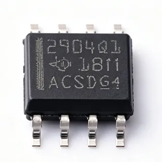
LM2904BIDR - Dual 36V 1.2MHz Op Amp | SOIC-10 | TI
MPN: LM2904BIDR ✓ Active| Qty | Unit Price | Extended |
|---|---|---|
| 1 | $0.42 | $0.42 |
| 10 | $0.34 | $3.40 |
| 100 | $0.22 | $22.00 |
| 500 | $0.18 | $90.00 |
| 1,000 | $0.15 | $150.00 |
| 2,500 | $0.13 | $325.00 |
LM2904BIDR Overview
An operational amplifier (op amp) is a high-gain DC-coupled differential amplifier whose output voltage is amplified by an external feedback network to perform amplification, filtering, and signal conditioning. A dual op amp integrates two ICs into a single package and is the same circuit-level topology (LDO) integrated with a higher-level power-supply chain and ultimately a semiconductor device, while dual op amps specifically serve as a low-side companion building block used in many sensor, instrumentation, and power-management signal chains.
Key features include 1.2 MHz gain-bandwidth product, 0.5 mV typical (3 mV maximum) input offset voltage, 45 V/us (typical) slew rate, 25 nA input bias current, and an output swing that includes both rails. The device operates on a single supply from 3 V up to 36 V (or dual +/-1.5 V to +/-18 V). It is internally compensated for unity-gain stability and includes short-circuit protection on the output, making it suitable for direct drive of low-impedance loads in industrial and automotive environments.
The LM2904BIDR uses a bipolar process with a PNP input stage that supports input common-mode voltages down to ground (and up to VCC - 1.5 V), enabling true single-supply operation from a 5 V or 12 V rail. The dual-channel architecture allows one IC to implement two independent gain stages - commonly a transimpedance amplifier and a buffer, or two channels of a differential sensor front-end - saving PCB area, cost, and complexity versus using two single-channel op amps.
Typical applications include transducer interfaces (load cells, strain gauges, pressure and flow sensors), low-side current sensing in motor drives and battery management, active filters and integrators for instrumentation, comparator-like threshold detection, and general-purpose signal conditioning on 12 V / 24 V industrial and automotive buses. The wide supply range and automotive-grade temperature rating make it drop-in compatible with virtually every legacy LM288 / LM358 / LM2904 design.
When designing with this device, ensure the input common-mode voltage remains within the linear range (GND to VCC - 1.5 V). For single-supply designs, AC-couple the input or bias the network to mid-supply. Decouple the supply pin with a 1 uF / 100 nF parallel pair within 10 mm of the IC, and avoid driving capacitive loads greater than 1 nF directly - add a series isolation resistor if needed.
This page synthesizes distributor pricing, drop-in alternatives, and practical design notes not found in the manufacturer datasheet, giving you a complete engineering perspective in one page.
Drop-in alternatives for LM2904BIDR — same package, pin-to-pin compatible. Different-package parts requiring PCB rework are excluded.
Variants in this series
Same-series models that are drop-in compatible with LM2904BIDR (same form factor and footprint) — differing in Slew Rate, Package, Amplifier Type, Operating Temperature, Gain Bandwidth Product.
Quick Comparison Tool — Select alternative parts for side-by-side comparison:
LM2904DR
✅ Drop-In✓ In Stock
$0.1 / Unit
View Datasheet →LM358DR
✅ Drop-In✓ In Stock
$0.0514 / Unit
View Datasheet →LM2904BQDRQ1
✅ Drop-In📋 Reference alternative (not in catalog)
LM2904AYDT
✅ Drop-In📋 Reference alternative (not in catalog)
LM2904DR2G
✅ Drop-In📋 Reference alternative (not in catalog)
NJM2904M
✅ Drop-In📋 Reference alternative (not in catalog)
LM2904BIDR Maximum Ratings & Electrical Characteristics
| Manufacturer | Texas Instruments |
| Function | Industry-standard dual operational amplifier |
| Number of Channels | 2 (Dual) |
| Supply Voltage Range (Single) | 3 V to 36 V |
| Supply Voltage Range (Dual) | +/-1.5 V to +/-18 V |
| Gain-Bandwidth Product (GBW) | 1.2 MHz |
| Slew Rate | 0.5 V/us (typical) |
| Input Offset Voltage | 0.5 mV typical / 3 mV maximum |
| Input Bias Current | 25 nA typical |
| Input Common-Mode Range | GND to VCC - 1.5 V (single supply) |
| Output Swing | Rail-to-rail output |
| Operating Temperature Range | -40 C to +125 C |
| Package | SOIC-8 (D) |
| Mounting Type | Surface Mount |
| MSL Level | 1 (Unlimited) |
| RoHS Status | Compliant |
| Lead-Free | Yes |
LM2904BIDR Pin Configuration
| Pin 1 | OUT A — Output of amplifier A |
| Pin 2 | IN- A — Inverting input of amplifier A |
| Pin 3 | IN+ A — Non-inverting input of amplifier A |
| Pin 4 | VCC- / GND — Negative supply or ground for single-supply operation |
| Pin 5 | IN+ B — Non-inverting input of amplifier B |
| Pin 6 | IN- B — Inverting input of amplifier B |
| Pin 7 | OUT B — Output of amplifier B |
| Pin 8 | VCC+ — Positive supply voltage |
Typical Applications
LM2904BIDR is suitable for 6 applications: Automotive Sensor Signal Conditioning, Industrial 24V PLC Analog Input Module, Active Filter and Integrator for Instrumentation, Low-Side Current Sensing for Motor Drive, Threshold Detector and Window Comparator, General-Purpose Signal Conditioning and Buffers.
Automotive Sensor Signal Conditioning
The LM2904BIDR's wide 3 V to 36 V supply range and -40 C to +125 C automotive temperature rating make it ideal for conditioning automotive sensor signals on a 12 V battery bus. With 1.2 MHz GBW and 0.5 V/us slew rate, it can amplify pressure, position, and flow sensor signals up to ~100 kHz bandwidth without slew-rate limiting. The rail-to-rail output swing maximizes ADC dynamic range when powered from 5 V, and the 0.5 mV typical offset voltage minimizes calibration requirements in precision transducer interfaces. Used with a Wheatstone bridge sensor, a single channel provides gain of 100 to 1000 for a 0-5 V output swing. The dual channel allows simultaneous amplification of two sensors (e.g., pressure + temperature) on the same IC.
Recommended
Industrial 24V PLC Analog Input Module
The LM2904BIDR's 36 V supply tolerance and industrial -40 C to +125 C rating make it a workhorse for 24 V PLC analog input modules. With 1.2 MHz GBW, it can buffer 4-20 mA current-loop receivers and provide active filtering at the same time, reducing BOM count. The wide input common-mode range (GND to VCC - 1.5 V) allows direct connection to grounded sensors without level shifting. Used as a unity-gain buffer between a 4-20 mA receiver resistor and a 12-bit ADC, the LM2904BIDR provides low-impedance drive and input protection. The second channel can implement an active low-pass filter for 50/60 Hz mains noise rejection.
Recommended
Active Filter and Integrator for Instrumentation
The LM2904BIDR's 1.2 MHz GBW and 0.5 V/us slew rate make it well suited for active filters and integrators in instrumentation signal chains. With a unity-gain bandwidth 10x higher than the filter cutoff frequency, the LM2904BIDR introduces minimal phase shift and gain error in 100 kHz active low-pass or band-pass filters. The dual-channel architecture allows two filter stages (e.g., a Sallen-Key low-pass followed by a high-pass) in a single SOIC-8, saving PCB area versus cost. The 25 nA input bias current minimizes integrator drift in long-time-constant integrators with high-value feedback resistors.
Recommended
Low-Side Current Sensing for Motor Drive
The LM2904BIDR's wide supply range (3-36 V) and rail-to-rail output make it ideal for low-side current sensing in brushed DC and stepper motor drives. With 1.2 MHz GBW, it can amplify the 50-100 kHz PWM-edge current ripple on a shunt resistor without slew-rate distortion, providing clean current signals for FOC (Field Oriented Control) feedback loops. The dual-channel architecture allows simultaneous monitoring of two motor phases (e.g., phase A and phase B in a 3-phase inverter) on a single IC. The input common-mode range includes ground, so it can directly sense low-side shunts without biasing.
Recommended
Threshold Detector and Window Comparator
The LM2904BIDR's dual channels and wide supply range make it ideal for implementing window comparators and threshold detectors. With 1.2 MHz GBW and 0.5 V/us slew rate, it provides clean switching at the comparator trip point with minimal bounce. A single LM2904BIDR can implement two independent comparators (e.g., an under-voltage and over-voltage detector on a 12 V battery) without the cost of dedicated comparator ICs. The output swing includes both rails, so it directly drives 3.3 V or 5 V logic inputs without level translation. The 25 nA bias current minimizes input current errors in high-resistance voltage dividers.
Recommended
General-Purpose Signal Conditioning and Buffers
The LM2904BIDR is widely used as a general-purpose signal conditioner and unity-gain buffer in mixed-signal designs. With 1.2 MHz GBW, it can buffer ADC inputs, drive audio CODECs, or isolate high-impedance sensors from low-impedance loads without bandwidth limitation. The dual-channel architecture allows one channel for input signal buffering and the second for active filtering or gain stages. The wide 3-36 V supply range allows direct operation from 3.3 V, 5 V, 12 V, or 24 V rails without level shifting, simplifying power design. The rail-to-rail output maximizes dynamic range with low-voltage ADC references.
Recommended
Recommended Products Summary
Engineering reference data for LM2904BIDR — comparison, design guidance, and compliance information.
Selection Guide
Comparison with Alternatives
| Parameter | This Product | LM2904DR | LM358DR | LM2904BQDRQ1 | LM2904AYDT | LM2904DR2G | NJM2904M |
|---|---|---|---|---|---|---|---|
| Brand | Texas Instruments | Texas Instruments | Texas Instruments | Texas Instruments | STMicroelectronics | onsemi | NJR |
| Package | SOIC-8 (D) | SOIC-8 (D) - same | SOIC-8 (D) - same | SOIC-8 (D) - same | SOIC-8 (D) - same | SOIC-8 (D) - same | SOIC-8 (D) - same |
| Gain-Bandwidth Product | 1.2 MHz | 700 kHz | 1 MHz | 1.2 MHz | 1.1 MHz | 1 MHz | 1 MHz |
| Supply Voltage Range | 3 V to 36 V (single) | 3 V to 26 V | 3 V to 32 V | 3 V to 36 V | 3 V to 36 V | 3 V to 36 V | 3 V to 36 V |
| Input Offset Voltage (max) | 3 mV | 7 mV | 7 mV | 3 mV | 4 mV | 7 mV | 5 mV |
| Operating Temperature | -40 C to +125 C | -40 C to +125 C | 0 C to +70 C | -40 C to +125 C | -40 C to +125 C | -40 C to +125 C | -40 C to +85 C |
| AEC-Q100 Qualified | No | No | No | Yes | No | No | No |
| Output Swing | Rail-to-rail | Rail-to-rail (legacy) | Rail-to-rail (within 1.5 V) | Rail-to-rail | Rail-to-rail | Rail-to-rail | Rail-to-rail |
Key Differentiators
- Higher 1.2 MHz GBW vs legacy LM2904 700 kHz (vs LM2904DR)
- Tighter 3 mV max input offset voltage (vs LM2904DR)
- Automotive AEC-Q100 qualified option (vs LM2904BQDRQ1)
- Cross-brand drop-in compatibility (vs LM2904AYDT (STMicroelectronics))
Design Notes
Decouple the VCC+ pin (pin 8) with a 1 uF ceramic capacitor in parallel with a 100 nF ceramic capacitor, placed within 10 mm of the IC. The 1 uF bulk capacitor handles low-frequency transients while the 100 nF bypasses high-frequency noise. For dual-supply operation, also decouple VCC- (pin 4) with a 100 nF capacitor. Estimated: a single 100 nF bypass alone may not be sufficient above 1 MHz switching frequencies.
Do not drive capacitive loads greater than 1 nF directly - the LM2904BIDR output stage may oscillate. If a capacitive load is required (e.g., a long cable or large filter cap), place a 10-100 ohm isolation resistor in series with the output. The input common-mode range extends to ground but only up to VCC - 1.5 V; do not allow inputs to exceed VCC+ or go below VCC-, which can cause phase reversal or damage the input stage.
Use a ground plane on the bottom layer to provide a low-impedance return path for the input and output signals. Keep input traces short and away from output traces to minimize parasitic feedback that may cause oscillation. For high-gain configurations (gain > 100), use a ground guard trace around the input pins to minimize leakage currents from the supply rail or adjacent high-voltage signals.
For single-supply designs where the input signal is ground-referenced (e.g., a current shunt on the low-side of a load), AC-couple the input through a capacitor and bias the non-inverting input to mid-supply with a resistor divider. This ensures the input remains within the linear common-mode range (GND to VCC - 1.5 V). Estimated: a 10 Hz high-pass corner with 100 nF AC-coupling cap and 100 kohm bias resistors is a typical starting point for audio-bandwidth designs.
Compliance Information
RoHS compliant per TI product page. The LM2904BIDR is not AEC-Q100 qualified - choose LM2904BQDRQ1 for automotive applications. All industry-standard dual op amp parts in this family are lead-free and halogen-free per TI documentation.