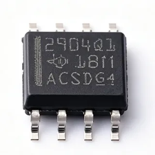
THS4031CDR - 100MHz Low-Noise Voltage Feedback Op Amp | TI
MPN: THS4031CDR ✓ Active| Qty | Unit Price | Extended |
|---|---|---|
| 1 | $1.85 | $1.85 |
| 10 | $1.66 | $16.60 |
| 100 | $1.42 | $142.00 |
| 500 | $1.24 | $620.00 |
| 1,000 | $1.05 | $1,050.00 |
THS4031CDR Overview
A voltage-feedback operational amplifier is a high-gain differential amplifier whose closed-loop bandwidth is set by the feedback network and the amplifier's gain-bandwidth product. Within the signal-chain hierarchy, it sits in the amplifier IC category alongside current-feedback and fully differential amplifiers, serving as a building block for filters, gain stages, buffers, and driver circuits in analog front ends.
Key features of the THS4031 include a 100 MHz bandwidth at a gain of 2, unity-gain stability with a 275 MHz open-loop bandwidth, an ultra-low input voltage noise of , and high DC precision with 90 dB CMRR. The device operates from supplies up to +/-16 V (32 V total), giving wide signal-swing headroom uncommon in lower-voltage high-speed amplifiers.
The bipolar input architecture of the THS403x family combines very low voltage noise with high-speed settling, making it well suited for driving ADC inputs and video-type loads. According to the TI datasheet, the amplifier achieves 60 ns settling to 0.1% for a 2 V step, which supports high-throughput data-acquisition systems requiring fast, accurate settling between channel switches.
Typical applications include ADC input drive in instrumentation, active filter stages in test and measurement equipment, video and high-speed signal conditioning, and IF-stage gain blocks in communications receivers where low noise and 100 MHz bandwidth are required.
Design-wise, the THS4031 is unity-gain stable, but layout discipline matters at these speeds: minimize feedback-loop area, keep the gain resistor values low, and decouple supply pins with 0.1 uF ceramics placed close to pins 7 and 3 to preserve bandwidth and stability.
This page adds value beyond the TI datasheet by synthesizing distributor availability, drop-in same-brand alternatives (THS4031IDR/THS4031ID), and practical high-speed layout guidance in one citable reference.
Drop-in alternatives for THS4031CDR — same package, pin-to-pin compatible. Different-package parts requiring PCB rework are excluded.
Variants in this series
Same-series models that are drop-in compatible with THS4031CDR (same form factor and footprint) — differing in Package.
Quick Comparison Tool — Select alternative parts for side-by-side comparison:
THS4031IDR
✅ Drop-In✓ In Stock
$2.62 / Unit
View Datasheet →THS4031IDR
✅ Drop-In✓ In Stock
$2.62 / Unit
View Datasheet →THS4031CDRG4
✅ Drop-In📋 Reference alternative (not in catalog)
THS4031IDG4
✅ Drop-In ⚠️ Specs Unverified📋 Reference alternative (not in catalog)
THS4021CD
✅ Drop-In ⚠️ Specs Unverified📋 Reference alternative (not in catalog)
THS4031CDR Maximum Ratings & Electrical Characteristics
| Amplifier Type | Voltage Feedback |
| Number of Channels | 1 |
| Bandwidth | 100 MHz (G = 2) |
| Unity-Gain Bandwidth | 275 MHz |
| Slew Rate | 100 V/us |
| Settling Time (0.1%) | 60 ns |
| CMRR | 90 dB |
| Supply Voltage Range | +/-16 V (32 V total) max |
| Operating Temperature Grade | 0C to 70C (C grade) |
| Package | SOIC-8 (D) |
| Mounting Type | Surface Mount |
| Packaging | Tape & Reel (R suffix) |
| Output Type | Single-ended, high drive capability |
| Stability | Unity-gain stable |
| Category | Linear - Amplifiers - Instrumentation, OP Amps, Buffer Amps |
THS4031CDR Pin Configuration
| Pin 1 | IN- — Inverting input |
| Pin 2 | IN+ — Non-inverting input |
| Pin 3 | V- — Negative power supply |
| Pin 4 | NC — Not connected (per datasheet) |
| Pin 5 | NC — Not connected (per datasheet) |
| Pin 6 | OUT — Amplifier output |
| Pin 7 | V+ — Positive power supply |
| Pin 8 | NC — Not connected (per datasheet) |
Typical Applications
THS4031CDR is suitable for 6 applications: ADC Input Drive in Data Acquisition, Active Filter Stages in Test and Measurement, Video and High-Speed Signal Conditioning, IF Gain Blocks in Communications Receivers, Precision Reference and Sensor Buffers, Industrial Automation Analog Front Ends.
ADC Input Drive in Data Acquisition
The THS4031CDR's 60 ns settling time to 0.1% and 100 MHz bandwidth make it an excellent buffer between a multiplexer or signal source and a high-speed analog-to-digital converter. In a typical data-acquisition front end, the amplifier is configured in a gain-of-1 or gain-of-2 non-inverting stage immediately ahead of the ADC input, isolating the converter's dynamic switched-capacitor load from the source impedance. The ultra-low input voltage noise preserves the effective-number-of-bits (ENOB) of a 12- to 14-bit converter, while the 100 V/us slew rate keeps large-signal inputs undistorted through full-scale steps. A small series isolation resistor and charge-kickback capacitor at the ADC pin dampens switching transients. Because the device tolerates supplies up to +/-16 V, it can drive converters requiring wide input swings without additional level shifting.
Recommended
Active Filter Stages in Test and Measurement
Test and measurement instruments rely on multiple-pole active low-pass and band-pass filters to condition signals before digitization, and the THS4031CDR is a strong fit for these gain blocks. Its 100 MHz bandwidth (G=2) provides ample open-loop headroom so that multiple-feedback and Sallen-Key filter stages maintain their designed corner frequency and Q up to tens of megahertz without bandwidth-induced peaking. The ultra-low voltage noise of the bipolar input stage minimizes the filter's own noise contribution, which matters when measuring microvolt-level signals. With +/-16 V supply capability, the amplifier offers wide output swing for measurement benches operating on +/-12 V or +/-15 V rails. Designers should use low-value resistors (hundreds of ohms to a few kilohms) in the filter network to keep resistor thermal noise and stray-capacitance effects below significance at video frequencies.
Recommended
Video and High-Speed Signal Conditioning
Video distribution, line driving, and high-speed signal conditioning benefit from the THS4031CDR's combination of 100 MHz bandwidth, 100 V/us slew rate, and high output drive. A standard-definition or high-definition video signal occupies bandwidth well inside the amplifier's flat region, so gain-of-2 (back-terminated 75-ohm cable driver) configurations maintain low differential gain and phase error across the video band. The unity-gain stability of the THS4031 means buffer configurations are safe without external compensation, and the 60 ns settling behavior prevents visible ghosting or smear after transients. In broadcast and surveillance equipment operating on +/-12 V rails, the wide supply range supports standard video output levels into back-terminated cables. Keep the feedback resistor around 1 kilohm or lower to avoid pole formation with input capacitance at 100 MHz.
Recommended
IF Gain Blocks in Communications Receivers
Intermediate-frequency (IF) stages in RF receivers require amplifiers with stable gain, low noise, and bandwidth comfortably above the IF; the THS4031CDR meets these needs for IFs in the tens of megahertz. Its low input voltage noise sets the noise figure contribution of the gain block, protecting receiver sensitivity when the amplifier follows a mixer or passive filter with insertion loss. The high CMRR of 90 dB rejects ground-borne interference common on dense receiver boards. Configured with a resistive gain set around 10 dB to 20 dB, the 100 MHz bandwidth provides substantial loop-gain margin at typical IFs, ensuring gain flatness and low distortion. The +/-16 V supply tolerance supports legacy communications hardware standardized on +/-15 V rails. DC-blocking capacitors should be sized to avoid low-frequency roll-off interaction with the amplifier's input bias network.
Recommended
Precision Reference and Sensor Buffers
Voltage references, bridge sensors, and photo-diode outputs need a low-noise, high-input-impedance buffer, and the THS4031CDR fills this role in systems that also require speed. The bipolar input stage offers ultra-low voltage noise, critical when buffering a precision reference whose noise directly modulates an ADC's full-scale accuracy. Its high input impedance loads the source negligibly, while the 100 MHz bandwidth ensures the buffer does not limit the response of fast-settling circuits such as sample-and-hold front ends or laser-diode modulation paths. In instrumentation running on +/-15 V rails, the wide supply range lets the buffer track references swinging close to the rails. Designers should add a 0.1 uF decoupling capacitor at each supply pin and route the sensitive input trace away from the output to preserve the 90 dB CMRR in guard-sensitive layouts.
Recommended
Industrial Automation Analog Front Ends
Factory automation systems condition signals from encoders, ultrasonic sensors, and current-sense circuits, and the THS4031IDR variant of this amplifier (same die, -40C to +125C) is the preferred choice for those environments. The amplifier's 100 MHz bandwidth handles fast pulse edges from ultrasonic and time-of-flight sensors, while the 100 V/us slew rate preserves edge fidelity for threshold comparators downstream. In 4-20 mA loop receivers, the amplifier converts the loop's sense-resistor voltage into a scaled signal for the ADC with low added noise. Boards on +/-12 V or +/-15 V industrial rails benefit from the +/-16 V supply tolerance. Use the C-grade THS4031CDR in climate-controlled cabinets (0C to 70C) and the I-grade sibling where panel mounting exposes the board to outdoor temperatures, with no PCB or layout changes required.
Recommended
Recommended Products Summary
Engineering reference data for THS4031CDR — comparison, design guidance, and compliance information.
Selection Guide
Comparison with Alternatives
| Parameter | This Product | THS4031IDR | THS4031ID | THS4031CDRG4 | THS4021CD |
|---|---|---|---|---|---|
| Package | SOIC-8 (D) | SOIC-8 (D) - same | SOIC-8 (D) - same | SOIC-8 (D) - same | SOIC-8 (D) - same |
| Brand | Texas Instruments | Texas Instruments | Texas Instruments | Texas Instruments | Texas Instruments |
| Bandwidth (G=2) | 100 MHz | 100 MHz | 100 MHz | 100 MHz | 550 MHz |
| Operating Temperature | 0C to 70C | -40C to 125C | -40C to 125C | 0C to 70C | 0C to 70C |
| Packaging Format | Tape & Reel | Tape & Reel | Tube/Tray | Tape & Reel | Tube/Tray |
Key Differentiators
- Lowest-noise option in the THS403x family (vs THS4021CD)
- Identical footprint across temperature grades (vs THS4031IDR)
- Fast settling for multiplexed acquisition (vs THS4021CD)
Design Notes
At 100 MHz bandwidth, layout discipline determines whether the THS4031CDR achieves datasheet performance. Keep the feedback loop as short and physically compact as possible to minimize stray inductance and capacitance; use gain-setting resistors of 1 kilohm or lower so that the pole formed with the input capacitance (roughly 2 pF) stays well above the band of interest. Place 0.1 uF ceramic decoupling capacitors within 2 mm of V+ (pin 7) and V- (pin 3), with a 2.2 uF to 10 uF bulk capacitor nearby on each rail.
The THS4031 is unity-gain stable, but voltage-feedback amplifiers lose phase margin when feedback resistance is high. Recommended: keep total feedback resistance (Rf + Rg) between 200 ohms and 2 kilohms. For gain-of-2 configurations, Rf = Rg = 1 kilohm is a proven starting point per the TI THS403x typical application circuits. If peaking appears in the frequency response, reduce feedback impedance or add a small capacitor (1-2 pF) across Rf to compensate the noise-gain pole.
Do not exceed the +/-16 V (32 V total) absolute-maximum supply, and never apply input signals beyond the supply rails even transiently, as the bipolar input stage can be damaged by input overvoltage without external clamp diodes. The C-grade 0C to 70C rating is frequently overlooked: a board that operates outdoors or near motors must use the I-grade THS4031IDR instead. Estimated: input protection series resistors of 100-500 ohms are advisable on any input that can be hot-plugged or externally connected.
Compliance Information
Compliance details were not present in the provided web data. Verify on the TI product quality/environmental page for THS4031CDR by date code.