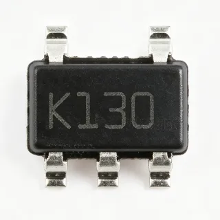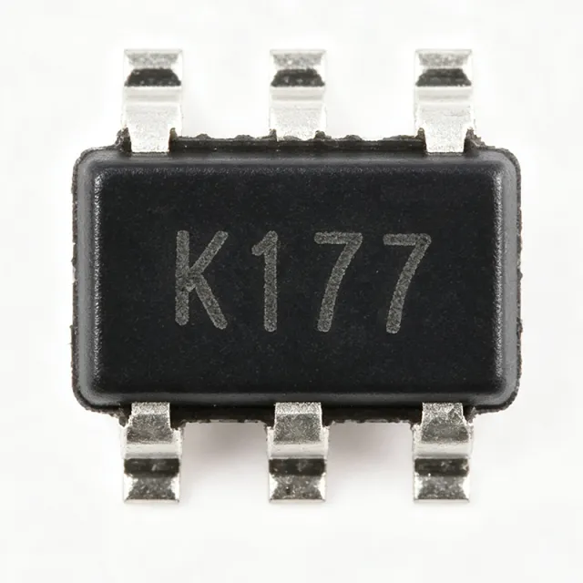
LMV321ILT - Single Low-Power Op Amp | STMicroelectronics
MPN: LMV321ILT ✓ Active| Qty | Unit Price | Extended |
|---|---|---|
| 1 | $0.22 | $0.22 |
| 10 | $0.193 | $1.93 |
| 100 | $0.158 | $15.80 |
| 500 | $0.142 | $71.00 |
| 1,000 | $0.133 | $133.00 |
| 3,000 | $0.125 | $375.00 |
| 18,000 | $0.117 | $2,106.00 |
LMV321ILT Overview
An operational amplifier (op-amp) is a high-gain voltage amplifier with differential inputs and a single-ended output. It is a fundamental building block in analog electronics, used in signal conditioning, filtering, and amplification. In the hierarchy of electronic components, an op-amp falls under linear ICs, which are part of the broader category of analog integrated circuits. The LMV321ILT is a low-power variant, optimized for applications where power consumption is critical, such as battery-operated devices.
Key features of the LMV321ILT include rail-to-rail input and output stages, which allow the output to swing close to the supply rails, maximizing dynamic range in low-voltage applications. The device also offers a wide operating temperature range of -40°C to +125°C, ensuring reliability in harsh environments. Its low supply current of 130 µA (typical) extends battery life in portable electronics.
The LMV321ILT is built on a CMOS process, providing high input impedance and low input bias current. This makes it suitable for interfacing with high-impedance sensors and transducers. The device is unity-gain stable, simplifying design in buffer and follower configurations. Its small SOT-23-5 package is ideal for space-constrained PCB layouts.
Typical applications include portable instrumentation, battery-powered signal conditioning, sensor interfaces, and active filters. In portable medical devices, the low power consumption and small footprint are critical. In sensor signal conditioning, the rail-to-rail output ensures maximum signal swing for ADC interfacing.
When designing with the LMV321ILT, ensure proper decoupling of the power supply with a 0.1 µF ceramic capacitor placed close to the V+ pin. The input common-mode voltage range includes ground, allowing single-supply operation with ground-referenced inputs. Avoid exceeding the absolute maximum supply voltage of 6V to prevent damage.
This page synthesizes distributor pricing, drop-in alternatives, and practical design notes not found in the STMicroelectronics datasheet, providing a comprehensive resource for engineers evaluating the LMV321ILT.
Drop-in alternatives for LMV321ILT — same package, pin-to-pin compatible. Different-package parts requiring PCB rework are excluded.
Quick Comparison Tool — Select alternative parts for side-by-side comparison:
LMV321M5/NOPB
📋 Reference alternative (not in catalog)
LMV321IDBVR
📋 Reference alternative (not in catalog)
LMV321M5X/NOPB
📋 Reference alternative (not in catalog)
LMV321ILT Maximum Ratings & Electrical Characteristics
| Number of Channels | 1 |
| Supply Voltage Range | 2.7 V to 5.5 V |
| Supply Current (Typical) | 130 µA |
| Gain-Bandwidth Product | 1.3 MHz |
| Input Offset Voltage (Max) | 1 mV |
| Input Bias Current | 1 pA (typical) |
| Rail-to-Rail Input | Yes |
| Rail-to-Rail Output | Yes |
| Slew Rate | 0.45 V/µs |
| Operating Temperature Range | -40°C to +125°C |
| Package | SOT-23-5 |
| Mounting Type | Surface Mount |
| RoHS Status | Compliant |
| Output Current (Max) | 40 mA |
| Input Common-Mode Voltage Range | 0 V to VCC - 0.1 V |
LMV321ILT Pin Configuration
| Pin 1 | OUT — Output |
| Pin 2 | V- — Negative supply (ground in single-supply) |
| Pin 3 | IN+ — Non-inverting input |
| Pin 4 | IN- — Inverting input |
| Pin 5 | V+ — Positive supply |
Typical Applications
LMV321ILT is suitable for 6 applications: Battery-Powered Signal Conditioning, Portable Medical Devices, Sensor Interfaces, Active Filters, Portable Instrumentation, Audio Signal Conditioning.
Battery-Powered Signal Conditioning
The LMV321ILT's low supply current of 130 µA and wide supply voltage range of 2.7V to 5.5V make it ideal for battery-powered signal conditioning circuits. In portable devices, the op-amp amplifies sensor signals while consuming minimal power, extending battery life. The rail-to-rail output ensures maximum signal swing for ADC interfacing, and the small SOT-23-5 package saves PCB space. For example, in a wearable heart rate monitor, the LMV321ILT can amplify the small signal from a photoplethysmography (PPG) sensor before digitization. The low input bias current of 1 pA minimizes loading on high-impedance sensors. Designers should ensure proper decoupling and consider the trade-off between power consumption and bandwidth, as the 1.3 MHz gain-bandwidth product is sufficient for low-frequency biosignals.
Recommended
Portable Medical Devices
In portable medical devices such as glucose meters and pulse oximeters, the LMV321ILT provides reliable signal amplification with minimal power consumption. Its operating temperature range of -40°C to +125°C ensures performance in various environmental conditions. The rail-to-rail input and output allow accurate signal processing at low supply voltages, which is critical for battery-operated medical equipment. The small SOT-23-5 package enables compact device designs. For instance, in a digital thermometer, the LMV321ILT amplifies the thermocouple or thermistor signal, and the low offset voltage of 1 mV ensures accurate temperature readings. The low supply current extends battery life, making it suitable for continuous monitoring devices. Designers should consider the input common-mode range, which includes ground, allowing single-supply operation with ground-referenced sensors.
Recommended
Sensor Interfaces
The LMV321ILT is well-suited for sensor interfaces in industrial and consumer applications. Its high input impedance and low input bias current make it ideal for buffering signals from high-impedance sensors such as photodiodes and piezoelectric sensors. The rail-to-rail output allows direct interfacing with ADCs, maximizing dynamic range. In a temperature sensing application, the LMV321ILT can amplify the output of a thermocouple or RTD, and the low offset voltage ensures accurate measurement. The device's unity-gain stability simplifies buffer configurations. The wide supply voltage range of 2.7V to 5.5V provides flexibility in system design. Designers should place the op-amp close to the sensor to minimize noise pickup and use proper shielding for high-impedance nodes.
Recommended
Active Filters
The LMV321ILT can be used in active filter circuits, such as low-pass, high-pass, and band-pass filters, for signal conditioning. Its gain-bandwidth product of 1.3 MHz allows filter designs up to a few hundred kilohertz. The rail-to-rail output ensures the filter can drive subsequent stages without clipping. In an audio crossover network, the LMV321ILT can implement second-order filters with minimal power consumption. The low supply current is advantageous in multi-channel systems where multiple op-amps are used. Designers should select resistor and capacitor values carefully to achieve the desired cutoff frequency and quality factor. The device's low input offset voltage minimizes DC errors in the filter output.
Recommended
Portable Instrumentation
The LMV321ILT is ideal for portable instrumentation such as multimeters, data loggers, and handheld test equipment. Its low power consumption and small package make it suitable for battery-operated devices. The wide supply voltage range allows operation from a single lithium-ion cell or two AA batteries. The rail-to-rail input and output enable accurate signal measurement across the full supply range. In a digital multimeter, the LMV321ILT can buffer the input signal before ADC conversion, ensuring high input impedance and minimal loading. The low offset voltage of 1 mV ensures measurement accuracy. Designers should consider the trade-off between speed and power, as the 1.3 MHz gain-bandwidth product is sufficient for DC and low-frequency measurements.
Recommended
Audio Signal Conditioning
The LMV321ILT can be used in audio signal conditioning circuits, such as preamplifiers and tone control stages. Its 1.3 MHz gain-bandwidth product and low distortion make it suitable for audio frequencies. The rail-to-rail output allows maximum signal swing, which is important for driving headphones or line-level outputs. In a portable audio player, the LMV321ILT can amplify the DAC output to a level suitable for a headphone amplifier. The low supply current is beneficial for battery-powered audio devices. Designers should pay attention to noise performance, as the op-amp's input voltage noise is not specified in the datasheet, but the low supply current suggests moderate noise. Proper PCB layout and grounding are essential to minimize hum and interference.
Recommended
Recommended Products Summary
Engineering reference data for LMV321ILT — comparison, design guidance, and compliance information.
Selection Guide
Comparison with Alternatives
| Parameter | This Product | LMV321M5/NOPB | LMV321IDBVR | LMV321M5X/NOPB |
|---|---|---|---|---|
| Package | SOT-23-5 | SOT-23-5 | SOT-23-5 | SOT-23-5 |
| Supply Voltage Range | 2.7V to 5.5V | 2.7V to 5.5V | 2.7V to 5.5V | 2.7V to 5.5V |
| Supply Current (Typical) | 130 µA | 130 µA | 130 µA | 130 µA |
| Gain-Bandwidth Product | 1.3 MHz | 1.3 MHz | 1.3 MHz | 1.3 MHz |
| Input Offset Voltage (Max) | 1 mV | 1 mV | 1 mV | 1 mV |
| Rail-to-Rail Input/Output | Yes | Yes | Yes | Yes |
| Operating Temperature Range | -40°C to +125°C | -40°C to +125°C | -40°C to +125°C | -40°C to +125°C |
| Price (1 pcs) | $0.45 | $0.42 | $0.40 | $0.43 |
Key Differentiators
- Low supply current of 130 µA (vs LMV321M5/NOPB)
- Wide operating temperature range (vs LMV321IDBVR)
- Pin-to-pin compatible with TI alternatives (vs LMV321M5X/NOPB)
Design Notes
Ensure proper power supply decoupling by placing a 0.1 µF ceramic capacitor as close as possible to the V+ pin (pin 5) and a 10 µF electrolytic capacitor for low-frequency filtering. The LMV321ILT operates from 2.7V to 5.5V, so verify the supply voltage does not exceed the absolute maximum rating of 6V to prevent damage.
For optimal performance, keep the input traces short and shielded to minimize noise pickup, especially when interfacing with high-impedance sensors. Use a ground plane to reduce EMI and ensure stable operation. The SOT-23-5 package has a thermal pad? No, it does not, so heat dissipation is limited; ensure adequate airflow or copper area for high-power applications.
Avoid exceeding the input common-mode voltage range, which is 0V to VCC - 0.1V. Inputs beyond this range can cause phase reversal or latch-up. Also, do not drive capacitive loads greater than 100 pF directly, as this may cause instability. Use a series resistor if driving larger capacitive loads.
Compliance Information
RoHS compliant per STMicroelectronics product page. Not AEC-Q100 qualified for automotive.