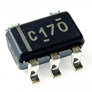
SN74LVC1G17DBVR - Schmitt-Trigger Buffer 5.5V | TI
MPN: SN74LVC1G17DBVR ✓ Active| Qty | Unit Price | Extended |
|---|---|---|
| 1 | $0.29 | $0.29 |
| 10 | $0.24 | $2.40 |
| 100 | $0.12 | $12.00 |
| 500 | $0.09 | $45.00 |
| 1,000 | $0.07 | $70.00 |
SN74LVC1G17DBVR Overview
A Schmitt-trigger buffer is a logic device that uses positive feedback to create hysteresis, giving it two distinct switching thresholds for rising and falling edges. Within the logic IC hierarchy, it belongs to the buffer/line-driver family of standard logic, used to isolate, drive, and condition digital signals. Hysteresis makes it ideal for cleaning up noisy signals, squaring off slow edges, and converting slowly changing analog inputs into crisp digital logic levels.
Key features include the wide 1.65 V to 5.5 V supply range for compatibility with 3.3 V and 5 V systems, high CMOS output drive of up to 32 mA at 3.3 V, and low static power dissipation. The device is fully specified for partial-power-down applications using Ioff, which prevents damaging backflow current when VCC is removed. Per TI datasheet, the same die is also available in the ultra-small 0.64 mm2 DPW package with 0.5 mm pitch and in SC70 options.
The SN74LVC1G17 is fabricated in CMOS technology, combining high-speed operation with low power. Schmitt-trigger inputs provide typical hysteresis of approximately 0.4 V at 3.3 V, ensuring clean switching with slow or noisy inputs, while the push-pull output directly drives LEDs, relay drivers, or downstream logic inputs without external pull resistors.
Typical applications include sensor signal conditioning, switch debouncing, level shifting between logic families, oscillator circuits, and clock buffering in industrial and consumer designs spanning both 3.3 V and 5 V rails.
Design tip: keep input signals within the supply range to avoid latch-up, and place the device close to the signal source to minimize trace inductance in high-speed paths. Pricing and stock data are current as of 2026-08-30.
Drop-in alternatives for SN74LVC1G17DBVR — same package, pin-to-pin compatible. Different-package parts requiring PCB rework are excluded.
Variants in this series
Same-series models that are drop-in compatible with SN74LVC1G17DBVR (same form factor and footprint) — differing in Package, RoHS Status, Logic Function, Technology.
Quick Comparison Tool — Select alternative parts for side-by-side comparison:
SN74LVC1G17QDBVRQ1
✅ Drop-In✓ In Stock
$0.09 / Unit
View Datasheet →SN74LVC1G17DBVT
✅ Drop-In📋 Reference alternative (not in catalog)
SN74AUP1G17DBVR
⚡ Same Package📋 Reference alternative (not in catalog)
74LVC1G17GV,125
✅ Drop-In📋 Reference alternative (not in catalog)
MC74VHC1GT17DTR2G
✅ Drop-In📋 Reference alternative (not in catalog)
SN74LVC1G17DBVR Maximum Ratings & Electrical Characteristics
| Logic Function | Non-inverting buffer (Y = A) |
| Schmitt-Trigger Input | Yes |
| Supply Voltage Range | 1.65 V to 5.5 V |
| Output Type | Push-Pull |
| Output Current | up to 32 mA at 3.3 V |
| Number of Elements | 1 |
| Bits per Element | 1 |
| Ioff (Partial Power Down) | Yes |
| Input Hysteresis | Approximately 0.4 V typical at 3.3 V |
| Technology | CMOS (LVC) |
| Package | SOT-23-5 (DBV) |
| Mounting Type | Surface Mount |
| MSL Level | 1 (260C unlimited) |
| RoHS Status | Compliant |
| Alternative Packages | DPW 0.64 mm2 (0.5 mm pitch), SC70 |
SN74LVC1G17DBVR Pin Configuration
| Pin 1 | A — Schmitt-trigger input |
| Pin 2 | GND — Ground |
| Pin 3 | Y — Push-pull output (Y = A) |
| Pin 4 | VCC — Power supply, 1.65 V to 5.5 V |
| Pin 5 | NC — No internal connection |
Typical Applications
SN74LVC1G17DBVR is suitable for 6 applications: Sensor Signal Conditioning, Switch Debouncing, Clock Buffering, Automotive Signal Interface, Level Shifting Between Logic Families, Oscillator and RC Timing Circuits.
Sensor Signal Conditioning
The SN74LVC1G17DBVR converts slow or noisy analog-like sensor outputs into clean digital levels thanks to Schmitt-trigger input hysteresis of roughly 0.4 V at 3.3 V. Placed immediately after the sensor, it squares rising edges from RC-filtered comparators, photodetectors, or encoder outputs. The 1.65 V to 5.5 V supply range lets one buffer serve both 3.3 V and 5 V sensor domains, and its push-pull 32 mA output at 3.3 V drives downstream counters or MCU inputs without pull resistors.
Recommended
Switch Debouncing
Mechanical switches bounce for milliseconds, producing false edges; the Schmitt-trigger buffer removes both bounce-induced chatter and slow RC edges. A typical circuit places an RC filter (e.g., 10 kOhm with 100 nF) after the switch, then the SN74LVC1G17DBVR squares the filtered waveform into a crisp edge for MCU GPIO or counters. The wide 1.65 V to 5.5 V supply range and Ioff partial-power-down support make it flexible across 3.3 V and 5 V industrial panels, and the SOT-23-5 package fits tight button-interface PCBs.
Recommended
Clock Buffering
A single clock distribution point often drives multiple loads; the SN74LVC1G17DBVR buffers the oscillator or MCU clock output, restoring edges and isolating load capacitance. Its CMOS push-pull output drives up to 32 mA at 3.3 V, enough for several gate inputs or a transmission line with series termination. Low static power keeps idle clock trees efficient. For 5 V clock rails the full 5.5 V range applies. Place the buffer close to the oscillator to minimize trace inductance and preserve edge rates.
Recommended
Automotive Signal Interface
Using the AEC-Q100 qualified SN74LVC1G17QDBVRQ1 variant, this die shapes noisy automotive sensor and switch signals in 12 V systems stepped down to 5 V rails. Schmitt hysteresis rejects ground-noise-induced chatter common in vehicle harnesses, while Ioff protection prevents backflow when ECUs enter low-power modes. Push-pull 32 mA drive at 3.3 V feeds CAN transceiver enable pins or MCU inputs directly. The identical footprint to the commercial part lets one PCB layout serve both automotive and industrial builds.
Recommended
Level Shifting Between Logic Families
The SN74LVC1G17DBVR acts as a simple single-direction level interface when input thresholds of one logic family must meet another rail domain, given its TTL-compatible LVC input thresholds across a 1.65 V to 5.5 V supply. Fed by a 3.3 V logic output while powered at 5 V, it outputs clean 5 V CMOS levels. Hysteresis prevents oscillation on slowly slewing translated edges. For bidirectional multi-bit translation, pair it with the LSF0101 or TXB0104 families instead.
Recommended
Oscillator and RC Timing Circuits
A Schmitt-trigger buffer with hysteresis enables classic relaxation oscillators: an RC network fed back from output Y to input A produces square waves with period set by R and C, typically in the kHz to MHz range depending on values. The SN74LVC1G17DBVR's well-defined thresholds (about 0.4 V hysteresis at 3.3 V) set predictable timing. CMOS low power keeps oscillator consumption minimal, and the SOT-23-5 footprint suits compact timing reference sections on industrial and consumer boards.
Recommended
Recommended Products Summary
Engineering reference data for SN74LVC1G17DBVR — comparison, design guidance, and compliance information.
Selection Guide
Comparison with Alternatives
| Parameter | This Product | SN74LVC1G17QDBVRQ1 | 74LVC1G17GV,125 | MC74VHC1GT17DTR2G | SN74AUP1G17DBVR |
|---|---|---|---|---|---|
| Package | SOT-23-5 (DBV) | SOT-23-5 (DBV) - same | SOT-23-5 - same | SOT-23-5 - same | SOT-23-5 (DBV) - same |
| Brand | Texas Instruments | Texas Instruments | Nexperia | onsemi | Texas Instruments |
| Supply Voltage Range | 1.65 V to 5.5 V | 1.65 V to 5.5 V | 1.65 V to 5.5 V | 2.0 V to 5.5 V | 0.8 V to 3.6 V |
| Logic Function | Buffer, non-inverting (Y = A) | Buffer, non-inverting | Buffer, non-inverting | Buffer, non-inverting | Buffer, non-inverting |
| Ioff Partial Power-Down | Yes | Yes | Yes | No | Yes |
| Automotive Grade | No | Yes (AEC-Q100) | No | No | No |
Key Differentiators
- Full 1.65 V to 5.5 V supply range (vs SN74AUP1G17DBVR)
- High output drive with Ioff (vs SN74AUP1G17DBVR)
- Automotive qualified variant available on same footprint (vs SN74LVC1G17QDBVRQ1)
Design Notes
Place the SN74LVC1G17DBVR close to the signal source or the noisy input node. Long traces before a Schmitt input pick up ringing and ground bounce that can add delay jitter; buffering at the source preserves the hysteresis advantage. Use series termination (22-33 ohm) when driving transmission lines from the push-pull 32 mA output.
Decouple VCC with a 100 nF ceramic capacitor placed within 5 mm of pin 4 to ground. Because the device is a single gate, switching current is modest, but shared decoupling with high-drive devices can couple noise into the analog-referenced input threshold - give it its own local capacitor on mixed-signal boards.
Keep the input signal within GND to VCC to avoid latch-up; LVC inputs tolerate 0 to 5.5 V only within the specified VCC conditions. Also remember the SN74AUP1G17 and SN74AUC1G17 (per TI E2E) have much lower drive strength and lower VCC maximums - do not substitute them blindly in 5 V designs.
Compliance Information
RoHS compliant and MSL 1 per distributor data (PartGenie). AEC-Q100 variant available separately (SN74LVC1G17QDBVRQ1). REACH/halogen status not found in provided data.