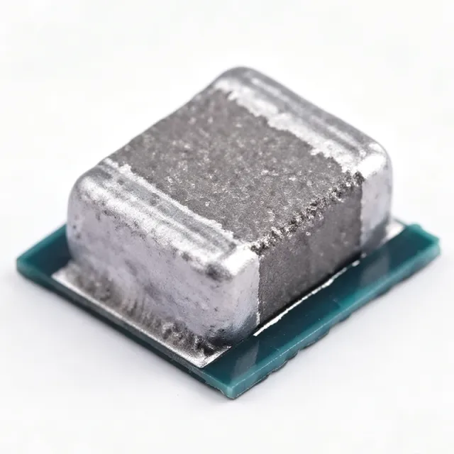
TPS82130SILR - 17V 3A Step-Down MicroSiP Module | Texas Instruments
MPN: TPS82130SILR ✓ Active| Qty | Unit Price | Extended |
|---|---|---|
| 1 | $3.44 | $3.44 |
| 10 | $3.1 | $31.00 |
| 100 | $2.75 | $275.00 |
| 500 | $2.45 | $1,225.00 |
| 1,000 | $2.18 | $2,180.00 |
TPS82130SILR Overview
A step-down converter, also called a buck converter, is a switching DC-DC voltage regulator that converts a higher input voltage to a lower output voltage with high efficiency. Buck converters form a core building block of power management IC hierarchies, sitting alongside LDOs, charge pumps, and power modules. The TPS82130 further collapses discrete switching FETs, inductor, and loop compensation into a single micro module, dramatically reducing external component count and PCB area compared to discrete regulator designs that require external FETs, a power inductor, and compensation components.
Key features include the wide 3V-17V input range that supports 12V and 5V bus systems, 3A continuous output, adjustable 0.9V-5V output via external resistor divider, 2.2MHz fixed switching frequency that allows small external capacitors, internal soft-start for inrush current limiting, a power-good output flag for sequencing, an enable pin for shutdown control, and thermal shutdown protection. The MicroSiP package exposes a bottom thermal pad that routes heat directly into the PCB copper pour.
Technically, the TPS82130 uses fixed-frequency peak-current-mode control, providing fast transient response and stability with minimal output capacitance (typically 22uF ceramic). It supports 100% duty cycle operation for low dropout at high VIN-to-VOUT ratios. The integrated shielded inductor reduces radiated EMI while simplifying PCB layout, and the low 1.5mm profile suits automated assembly with standard surface-mount equipment.
Typical applications include point-of-load (POL) power for FPGAs, DSPs, and ASICs in industrial systems, factory automation sensor supplies, 12V-rail distributed power in IoT edge nodes, and portable test equipment where small solution size is critical.
When designing, follow the datasheet recommendations for input and output ceramic capacitance, place the module close to the load, and provide a generous copper area under the thermal pad, especially at high output currents. Pricing references apply as of 2026-08-28.
This page synthesizes distributor pricing, drop-in alternatives, and practical design notes not found in the manufacturer datasheet.
Drop-in alternatives for TPS82130SILR — same package, pin-to-pin compatible. Different-package parts requiring PCB rework are excluded.
Variants in this series
Same-series models that are drop-in compatible with TPS82130SILR (same form factor and footprint) — differing in Continuous Output Current, MSL Level, Output Voltage Range, Package, Switching Frequency.
Quick Comparison Tool — Select alternative parts for side-by-side comparison:
TPS82140SILR
✅ Drop-In✓ In Stock
$2.45 / Unit
View Datasheet →TPS82150SILR
✅ Drop-In📋 Reference alternative (not in catalog)
TPS82130SILT
✅ Drop-In📋 Reference alternative (not in catalog)
TPS82130SILR Maximum Ratings & Electrical Characteristics
| Topology | Synchronous Buck (Step-Down) |
| Module Type | MicroSiP Power Module (integrated inductor and FETs) |
| Input Voltage Range | 3 V to 17 V |
| Output Voltage Range | 0.9 V to 5 V (adjustable) |
| Continuous Output Current | 3 A |
| Switching Frequency | 2.2 MHz (typical, fixed) |
| Control Mode | Peak Current Mode |
| Efficiency (typical) | >90% at moderate load |
| Soft-Start | Internal |
| Power Good Output | Yes |
| Enable Pin | Yes (active-high) |
| Thermal Shutdown | Yes |
| Operating Temperature Range | -40C to +125C |
| Package | 8-pin uSIP (SIL) 3.0mm x 2.8mm x 1.5mm |
| Mounting Type | Surface Mount |
| MSL Level | 2 (1 year floor life) |
| RoHS Status | Compliant |
TPS82130SILR Pin Configuration
| Pin 1 | VIN — Input supply voltage |
| Pin 2 | GND — Signal ground |
| Pin 3 | EN — Enable input (active high) |
| Pin 4 | PGND — Power ground |
| Pin 5 | FB — Feedback voltage input |
| Pin 6 | VOUT — Regulated output voltage |
| Pin 7 | PG — Power good output flag |
| Pin 8 | AGND — Analog ground |
Typical Applications
TPS82130SILR is suitable for 6 applications: FPGA Point-of-Load Power, Industrial Sensor and PLC Supplies, IoT Edge Devices and Gateway Nodes, Portable Test and Measurement Equipment, DSP and ASIC Core Power, Communication Equipment Power.
FPGA Point-of-Load Power
The TPS82130SILR is an ideal point-of-load supply for FPGA core and auxiliary rails in industrial embedded systems. With 3A continuous output, 0.9V to 5V adjustable output range, and a 3.0mm x 2.8mm uSIP footprint, it can power the FPGA core (typically 1.0V-1.2V), auxiliary (1.8V), and I/O (2.5V or 3.3V) rails from a single 12V bus. The 2.2MHz switching frequency avoids interfering with common FPGA clock harmonics around 100-500MHz, eliminating beat-frequency noise issues that plague lower-frequency regulators. Integrated synchronous FETs and shielded inductor eliminate 6-8 discrete components, dramatically reducing PCB area versus discrete buck designs.
Recommended
Industrial Sensor and PLC Supplies
The TPS82130SILR powers industrial 4-20mA loop transmitters, PLC analog input modules, and 24V-bus sensor conditioning circuits. Its 3V-17V input range directly accepts the 24V industrial bus (after protection/regulation) and 12V backplane rails commonly used in factory automation. The wide operating temperature range of -40C to +125C supports deployment in unconditioned factory environments. With internal thermal shutdown, power-good output, and enable pin for power sequencing, the TPS82130 provides the robustness required for industrial IEC 61010 environments. Typical efficiency above 90% minimizes thermal dissipation in sealed enclosures.
Recommended
IoT Edge Devices and Gateway Nodes
The TPS82130SILR fits compact IoT edge nodes and gateway designs that require multiple voltage rails in a small footprint. The integrated MicroSiP package occupies 75% less PCB area than equivalent discrete buck designs, freeing space for wireless modules, sensors, and battery management. With 3A peak capability, the TPS82130 can power a small SoC plus Wi-Fi/BLE radio module directly from a 12V or USB-C input. The 2.2MHz switching frequency enables small ceramic output capacitors (typically 22uF), and the internal soft-start limits inrush current that could trip upstream USB current-limit switches.
Recommended
Portable Test and Measurement Equipment
Handheld oscilloscopes, data loggers, and field test equipment benefit from the TPS82130SILR's compact size, high efficiency, and wide input range. Battery-powered instruments often use a 2-cell or 3-cell Li-ion pack (6V-12.6V) that maps directly to the TPS82130 input range. The 3A continuous capability powers analog front-end ADCs, FPGAs, and display backlight drivers simultaneously. The 1.5mm low-profile uSIP package allows the entire power tree to fit on the back side of small PCBs, leaving the top side for analog signal paths and user interface components. High efficiency above 90% extends battery runtime.
Recommended
DSP and ASIC Core Power
The TPS82130SILR is well-suited as a POL supply for DSP, ASIC, and high-performance microcontroller core rails. Modern DSPs often require 1.0V to 1.2V at 2-3A peak current with tight transient response - the TPS82130's peak-current-mode control delivers fast transient response with minimal output capacitance. The adjustable output from 0.9V to 5V covers virtually all DSP/ASIC core voltage requirements. The integrated power-good output enables sequencing with other system rails, and the enable pin allows shutdown to microampere-level quiescent current for sleep-mode applications. According to TI datasheet, the device supports 100% duty cycle for low-dropout operation at high VIN-VOUT deltas.
Recommended
Communication Equipment Power
Networking switches, wireless base stations, and small cell radio units can use the TPS82130SILR to power digital signal processors and baseband chips from 12V backplane rails. The 2.2MHz switching frequency and integrated shielded inductor minimize radiated EMI - critical for communication equipment that must meet FCC and CE conducted/radiated emissions limits. With 3A output capability, the TPS82130 powers baseband SoCs and DDR memory termination rails simultaneously. The small MicroSiP footprint allows power circuits to be placed directly beneath or adjacent to the load IC, minimizing parasitic inductance and improving transient response.
Recommended
Recommended Products Summary
Engineering reference data for TPS82130SILR — comparison, design guidance, and compliance information.
Selection Guide
Comparison with Alternatives
| Parameter | This Product | TPS82140SILR | TPS82150SILR | TPS82130SILT |
|---|---|---|---|---|
| Package | 8-pin uSIP (SIL) 3.0x2.8mm | 8-pin uSIP (SIL) 3.0x2.8mm - same | 8-pin uSIP (SIL) 3.0x2.8mm - same | 8-pin uSIP (SIL) 3.0x2.8mm - same |
| Brand | Texas Instruments | Texas Instruments | Texas Instruments | Texas Instruments |
| Output Current | 3 A | 2 A | 1 A | 3 A |
| Input Voltage Range | 3 V to 17 V | 3 V to 17 V | 3 V to 17 V | 3 V to 17 V |
| Output Voltage Range | 0.9 V to 5 V | 0.9 V to 5 V | 0.9 V to 5 V | 0.9 V to 5 V |
| Switching Frequency | 2.2 MHz | 2.2 MHz | 2.2 MHz | 2.2 MHz |
| Module Type | MicroSiP (integrated inductor) | MicroSiP (integrated inductor) | MicroSiP (integrated inductor) | MicroSiP (integrated inductor) |
Key Differentiators
- Highest output current in the TPS821xx uSIP family (vs TPS82140SILR)
- Same footprint, lower current for cost-down designs (vs TPS82150SILR)
- Integrated MicroSiP package eliminates 6-8 discrete components (vs Discrete TPS54360 buck design)
Design Notes
Estimated: At VIN=12V, VOUT=3.3V, and 3A load, the TPS82130SILR dissipates approximately (12-3.3) x 3 = 26.1 W of power. With adequate copper pour for the bottom thermal pad (datasheet recommends a minimum footprint pattern), junction-to-ambient thermal resistance is typically around 30-40 C/W, resulting in a 50-80 C temperature rise above ambient. For continuous 3A operation, follow the datasheet reference layout pattern exactly and use multiple thermal vias under the package's exposed pad to move heat into inner PCB layers.
Place the TPS82130SILR module close to the load IC, ideally within 5-10mm, to minimize parasitic inductance in the output loop. Use wide copper pours (at least 50mil) on VIN, VOUT, PGND, and the exposed thermal pad. Per the TI datasheet layout guidelines, place the input ceramic capacitor (typically 22uF X7R) as close as possible to the VIN pin, and place the output ceramic capacitor (typically 22uF X7R) directly at the VOUT pin. The AGND pin should be tied to the PGND pour at a single point near the output capacitor ground return.
Do not operate the TPS82130SILR above the absolute maximum VIN of 17V - transients on 12V industrial buses can exceed this during hot-plug events. Add a TVS diode or input voltage clamp if the design connects to long external cables. Do not omit the input capacitor: the TPS82130's high di/dt switching requires a low-ESR ceramic input cap to prevent VIN ringing. Per datasheet, use X7R/X5R ceramic capacitors - do not substitute Y5V which loses 60-80% of nominal capacitance at DC bias and temperature.
Keep the FB (feedback) trace away from noisy switching nodes (VIN, PGND, VOUT) and route it directly from the top of the output capacitor to the FB pin using a short, narrow trace surrounded by ground pour. Do not place the feedback divider resistors near the inductor - magnetic coupling can inject noise into the feedback path and cause output ripple or instability. The PG (power-good) output is an open-drain signal and requires an external pull-up resistor (typically 10k-100k) to VOUT or a logic rail.
Compliance Information
RoHS and REACH compliant per TI product page. Not AEC-Q100 qualified; choose TPS62150A-Q1 or similar -Q1 part for automotive applications.







