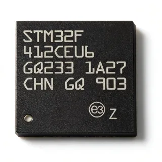
STM32F401CDU6 - ARM Cortex-M4F MCU 84MHz 384KB Flash | STMicroelectronics
MPN: STM32F401CDU6 ✓ Active| Qty | Unit Price | Extended |
|---|---|---|
| 1 | $4.5 | $4.50 |
| 10 | $4.05 | $40.50 |
| 100 | $3.6 | $360.00 |
| 500 | $3.15 | $1,575.00 |
| 1,000 | $2.7 | $2,700.00 |
STM32F401CDU6 Overview
An ARM Cortex-M4F microcontroller is a 32-bit processor core that includes a floating-point unit (FPU) and DSP instructions, making it suitable for applications requiring real-time signal processing and mathematical computations. The Cortex-M4F is part of the ARM Cortex-M family, which is widely used in embedded systems due to its energy efficiency and ease of development. The STM32F401CDU6 integrates this core with a comprehensive set of peripherals, including multiple USARTs, SPIs, I2Cs, ADCs, timers, and GPIOs, enabling it to serve as the central processing unit in complex embedded designs.
Key features of the STM32F401CDU6 include a maximum CPU frequency of 84 MHz, 384 KB of Flash memory, 96 KB of SRAM, and a rich set of communication interfaces: 3 USARTs, 4 SPIs, 3 I2Cs, and a USB 2.0 OTG FS. It also features a 12-bit ADC with up to 16 channels, 11 timers, and a random number generator (RNG). The device operates from a 1.7V to 3.6V power supply and supports a temperature range of -40°C to +85°C. The UFQFPN-48 package offers a compact solution with excellent thermal performance, making it ideal for space-constrained designs.
From a technical depth perspective, the STM32F401CDU6 is built on a 90nm process technology, which contributes to its low power consumption and high performance. The Cortex-M4F core includes a single-precision FPU and DSP instructions, enabling efficient execution of complex algorithms. The device also features a memory protection unit (MPU) for enhanced security and reliability. The STM32F401CDU6 supports a wide range of clock sources, including an external crystal, internal RC oscillators, and a PLL, allowing designers to optimize the clock configuration for their specific application.
Typical applications for the STM32F401CDU6 include industrial automation, where its robust communication interfaces and timers are used for motor control and process monitoring; consumer electronics, such as smart home devices and wearables, where its low power modes and compact package are advantageous; and IoT edge nodes, where its connectivity options and processing power enable data acquisition and local decision-making. The device is also well-suited for audio processing, thanks to its FPU and DSP capabilities.
When designing with the STM32F401CDU6, it is essential to provide adequate decoupling capacitors on the power supply pins and to follow the recommended PCB layout guidelines in the datasheet to ensure stable operation. The device supports multiple low-power modes, including Sleep, Stop, and Standby, which can be leveraged to minimize power consumption in battery-powered applications. Additionally, the STM32F401CDU6 is supported by the STM32Cube ecosystem, including HAL libraries and development tools, which accelerates firmware development and reduces time-to-market.
Drop-in alternatives for STM32F401CDU6 — same package, pin-to-pin compatible. Different-package parts requiring PCB rework are excluded.
Variants in this series
Same-series models that are drop-in compatible with STM32F401CDU6 (same form factor and footprint) — differing in Core, Flash Memory, Operating Temperature, SRAM, Timers.
Quick Comparison Tool — Select alternative parts for side-by-side comparison:
STM32F401CCU6
✅ Drop-In ⚠️ Specs Unverified📋 Reference alternative (not in catalog)
STM32F401CBU6
✅ Drop-In ⚠️ Specs Unverified📋 Reference alternative (not in catalog)
STM32F411CEU6
✅ Drop-In ⚠️ Specs Unverified✓ In Stock
$3.48 / Unit
View Datasheet →STM32F401CEU6
✅ Drop-In ⚠️ Specs Unverified✓ In Stock
$2.88 / Unit
View Datasheet →STM32F401CDU6TR
✅ Drop-In ⚠️ Specs Unverified📋 Reference alternative (not in catalog)
STM32F401CDU6 Maximum Ratings & Electrical Characteristics
| Core | ARM Cortex-M4F |
| Max Frequency | 84 MHz |
| Flash Memory | 384 KB |
| SRAM | 96 KB |
| Package | UFQFPN-48 (7x7 mm) |
| Operating Voltage | 1.7V to 3.6V |
| Operating Temperature | -40°C to +85°C |
| GPIO Pins | 36 |
| ADC | 12-bit, 16 channels |
| Timers | 11 |
| USART | 3 |
| SPI | 4 |
| I2C | 3 |
| USB | USB 2.0 OTG FS |
| DMA | Yes, 16 channels |
| RNG | Yes |
| RoHS | Compliant |
STM32F401CDU6 Pin Configuration
| Pin 1 | VBAT — Battery backup supply |
| Pin 2 | PC13 — GPIO / RTC |
| Pin 3 | PC14 — GPIO / OSC32_IN |
| Pin 4 | PC15 — GPIO / OSC32_OUT |
| Pin 5 | PF0 — GPIO / OSC_IN |
| Pin 6 | PF1 — GPIO / OSC_OUT |
| Pin 7 | NRST — Reset |
| Pin 8 | VDD — Power supply |
| Pin 9 | VSS — Ground |
| Pin 10 | PA0 — GPIO / ADC |
| Pin 11 | PA1 — GPIO / ADC |
| Pin 12 | PA2 — GPIO / USART2_TX |
| Pin 13 | PA3 — GPIO / USART2_RX |
| Pin 14 | PA4 — GPIO / SPI1_NSS |
| Pin 15 | PA5 — GPIO / SPI1_SCK |
| Pin 16 | PA6 — GPIO / SPI1_MISO |
| Pin 17 | PA7 — GPIO / SPI1_MOSI |
| Pin 18 | PB0 — GPIO / ADC |
| Pin 19 | PB1 — GPIO / ADC |
| Pin 20 | PB2 — GPIO / BOOT1 |
| Pin 21 | PB10 — GPIO / I2C2_SCL |
| Pin 22 | PB11 — GPIO / I2C2_SDA |
| Pin 23 | PB12 — GPIO / SPI2_NSS |
| Pin 24 | PB13 — GPIO / SPI2_SCK |
| Pin 25 | PB14 — GPIO / SPI2_MISO |
| Pin 26 | PB15 — GPIO / SPI2_MOSI |
| Pin 27 | PA8 — GPIO / MCO1 |
| Pin 28 | PA9 — GPIO / USART1_TX |
| Pin 29 | PA10 — GPIO / USART1_RX |
| Pin 30 | PA11 — GPIO / USB_DM |
| Pin 31 | PA12 — GPIO / USB_DP |
| Pin 32 | PA13 — GPIO / SWDIO |
| Pin 33 | PA14 — GPIO / SWCLK |
| Pin 34 | PA15 — GPIO / JTDI |
| Pin 35 | PB3 — GPIO / JTDO |
| Pin 36 | PB4 — GPIO / NJTRST |
| Pin 37 | PB5 — GPIO / I2C1_SMBA |
| Pin 38 | PB6 — GPIO / I2C1_SCL |
| Pin 39 | PB7 — GPIO / I2C1_SDA |
| Pin 40 | BOOT0 — Boot mode selection |
| Pin 41 | PB8 — GPIO / CAN_RX |
| Pin 42 | PB9 — GPIO / CAN_TX |
| Pin 43 | VDD — Power supply |
| Pin 44 | VSS — Ground |
| Pin 45 | PC0 — GPIO / ADC |
| Pin 46 | PC1 — GPIO / ADC |
| Pin 47 | PC2 — GPIO / ADC |
| Pin 48 | PC3 — GPIO / ADC |
Typical Applications
STM32F401CDU6 is suitable for 6 applications: Industrial Automation, IoT Edge Node, Consumer Electronics, Motor Control, Medical Devices, Audio Processing.
Industrial Automation
The STM32F401CDU6 is well-suited for industrial automation due to its robust communication interfaces (USART, SPI, I2C) and advanced timers for motor control. Its 84 MHz Cortex-M4F core with FPU enables precise real-time control of motors and process monitoring. The device's wide operating voltage range and industrial temperature range (-40°C to +85°C) ensure reliable operation in harsh environments. In a typical motor control application, the MCU generates PWM signals using its advanced timers, reads encoder feedback via GPIO or timer inputs, and communicates with a PLC via USART or CAN (through external transceiver). The FPU accelerates PID control algorithms, improving response time and accuracy. Compared to lower-end MCUs, the STM32F401CDU6 offers higher performance and more memory, allowing for more sophisticated control algorithms and data logging. Designers should ensure proper isolation and filtering on communication lines to prevent noise interference in industrial settings.
Recommended
IoT Edge Node
The STM32F401CDU6 is an excellent choice for IoT edge nodes, offering a balance of processing power, memory, and low power consumption. Its 384 KB Flash and 96 KB SRAM can accommodate communication stacks (e.g., MQTT, CoAP) and sensor data processing. The device supports multiple low-power modes (Sleep, Stop, Standby) to extend battery life. In a typical IoT node, the MCU collects data from sensors via I2C or SPI, processes it locally using the FPU, and transmits it to a gateway via Wi-Fi or LoRa (through external modules). The USB OTG interface can be used for device configuration or firmware updates. The compact UFQFPN-48 package is ideal for small form-factor designs. Designers should optimize the use of low-power modes and consider using an external RTC for time-stamping. The STM32F401CDU6's rich peripheral set reduces the need for external components, lowering BOM cost.
Recommended
Consumer Electronics
In consumer electronics, the STM32F401CDU6 is used in smart home devices, wearables, and audio equipment. Its Cortex-M4F core with FPU and DSP instructions enables audio processing, such as noise cancellation and equalization. The device's low power consumption and small package make it suitable for battery-powered wearables. For example, in a smart speaker, the MCU handles audio codec interfacing via I2S, processes audio data with the FPU, and controls user interface elements (LEDs, buttons). The USB OTG interface allows for firmware updates and data transfer. The STM32F401CDU6's rich peripheral set simplifies the design, reducing component count and board space. Designers should pay attention to audio quality by using proper grounding and decoupling techniques. The device's wide operating voltage range (1.7V to 3.6V) allows it to be powered directly from a Li-ion battery.
Recommended
Motor Control
The STM32F401CDU6 is ideal for motor control applications, including brushless DC (BLDC) motors and stepper motors. Its advanced timers can generate multiple PWM channels with dead-time insertion, and its 12-bit ADC can sample motor currents and voltages. The FPU accelerates field-oriented control (FOC) algorithms, enabling efficient and smooth motor operation. In a typical BLDC motor controller, the MCU generates six-step PWM signals, reads Hall sensor or encoder feedback, and implements current control loops. The device's 84 MHz clock ensures fast loop execution, and its DMA channels offload data transfer, reducing CPU load. The STM32F401CDU6's robust design includes protection features such as overcurrent detection via ADC and emergency stop via GPIO. Designers should implement proper gate driver circuits and snubbers to protect the MCU from voltage spikes. The device's wide temperature range makes it suitable for industrial motor drives.
Recommended
Medical Devices
The STM32F401CDU6 is used in medical devices such as patient monitors, infusion pumps, and diagnostic equipment. Its high performance and rich peripheral set enable real-time data acquisition and processing. The device's low power consumption is beneficial for portable medical devices. In a patient monitor, the MCU reads vital signs sensors (e.g., ECG, SpO2) via ADC or I2C, processes the signals using DSP instructions, and displays results on an LCD. The USB interface can be used for data logging and connectivity. The STM32F401CDU6's reliability and long-term availability make it suitable for medical applications. Designers must ensure compliance with medical standards (e.g., IEC 60601) and implement proper isolation and safety measures. The device's wide operating voltage range allows for battery backup systems.
Recommended
Audio Processing
The STM32F401CDU6 is well-suited for audio processing applications, including audio effects, voice recognition, and sound synthesis. Its Cortex-M4F core with FPU and DSP instructions can handle real-time audio algorithms, such as filtering, FFT, and echo cancellation. The device's I2S interface allows direct connection to audio codecs and DACs. In a typical audio effect pedal, the MCU reads audio samples via I2S, applies effects (e.g., reverb, distortion) using the FPU, and outputs the processed audio. The 84 MHz clock provides sufficient processing power for complex effects. The STM32F401CDU6's low latency and deterministic behavior are critical for real-time audio. Designers should use high-quality audio codecs and ensure proper grounding to minimize noise. The device's compact package is ideal for pedal enclosures.
Recommended
Recommended Products Summary
Engineering reference data for STM32F401CDU6 — comparison, design guidance, and compliance information.
Selection Guide
Comparison with Alternatives
| Parameter | This Product | STM32F401CCU6 | STM32F401CBU6 | STM32F411CEU6 | STM32F401CEU6 |
|---|---|---|---|---|---|
| Package | UFQFPN-48 (7x7 mm) | UFQFPN-48 (7x7 mm) - same | UFQFPN-48 (7x7 mm) - same | UFQFPN-48 (7x7 mm) - same | UFQFPN-48 (7x7 mm) - same |
| Brand | STMicroelectronics | STMicroelectronics | STMicroelectronics | STMicroelectronics | STMicroelectronics |
| Max Frequency | 84 MHz | 84 MHz | 84 MHz | 100 MHz | 84 MHz |
| Flash Memory | 384 KB | 256 KB | 128 KB | 512 KB | 512 KB |
| SRAM | 96 KB | 64 KB | 64 KB | 128 KB | 96 KB |
| USB | USB 2.0 OTG FS | USB 2.0 OTG FS | USB 2.0 OTG FS | USB 2.0 OTG FS | USB 2.0 OTG FS |
| ADC Channels | 16 | 16 | 16 | 16 | 16 |
| Timers | 11 | 11 | 11 | 11 | 11 |
Key Differentiators
- Higher memory capacity than STM32F401CCU6 (vs STM32F401CCU6)
- Lower cost than STM32F411CEU6 (vs STM32F411CEU6)
- Pin-compatible with other STM32F4 MCUs (vs STM32F401CBU6)
Design Notes
The STM32F401CDU6 operates from 1.7V to 3.6V. It is recommended to place a 100nF decoupling capacitor close to each VDD pin and a 4.7uF capacitor on the main VDD rail. For the VDDA pin, use a 1uF capacitor and a ferrite bead to isolate analog noise. The VBAT pin should be connected to a backup battery or tied to VDD through a diode to maintain RTC operation.
For the UFQFPN-48 package, ensure the exposed pad (EP) is soldered to a ground plane to improve thermal dissipation. Follow the recommended land pattern in the datasheet. Keep high-speed signals (e.g., SPI, USB) away from the crystal oscillator pins to avoid interference. Use a 4-layer PCB with dedicated ground and power planes for optimal performance.
Ensure the BOOT0 pin is properly configured to select the correct boot mode. If using SWD debugging, connect PA13 (SWDIO) and PA14 (SWCLK) with pull-up resistors. Do not leave unused GPIO pins floating; configure them as outputs or enable internal pull-ups/pull-downs to reduce power consumption. Also, verify that the external crystal load capacitors match the crystal's specification.
Compliance Information
RoHS compliant per STMicroelectronics product page. Not AEC-Q100 qualified.