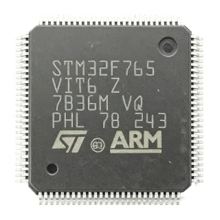
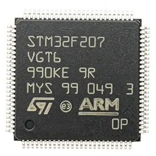
STM32F745VET6 - 32-bit ARM Cortex-M7 MCU, 512KB Flash | STMicroelectronics
MPN: STM32F745VET6 ✓ Active| Qty | Unit Price | Extended |
|---|---|---|
| 1 | $12.5 | $12.50 |
| 10 | $11.25 | $112.50 |
| 100 | $10 | $1,000.00 |
| 500 | $9 | $4,500.00 |
| 1,000 | $8.1 | $8,100.00 |
STM32F745VET6 Overview
What is a microcontroller? A microcontroller (MCU) is a compact integrated circuit designed to govern a specific operation in an embedded system. It integrates a processor core, memory (Flash and SRAM), and programmable input/output peripherals on a single chip. Microcontrollers are the backbone of modern embedded systems, ranging from simple household appliances to complex industrial automation and automotive control units. The STM32F745VET6 belongs to the STM32F7 series, which is part of the broader STM32 family of 32-bit Flash microcontrollers based on ARM Cortex-M cores. This hierarchy places it within the ARM Cortex-M7 category, known for its high performance and DSP capabilities.
Key features of the STM32F745VET6 include a 216 MHz Cortex-M7 core with double-precision floating-point unit (FPU), a comprehensive set of communication interfaces (USART, SPI, I2C, CAN, USB OTG, Ethernet MAC), advanced analog peripherals (3x 12-bit ADCs, 2x DACs), and a flexible memory controller supporting external SRAM, PSRAM, NOR, and NAND Flash. The device also includes a Chrom-ART Accelerator for enhanced graphical user interface performance, a cryptographic acceleration unit (AES, DES, 3DES, SHA-1, SHA-256, MD5), and a true random number generator (TRNG). These features make it ideal for applications requiring high-speed data processing, connectivity, and security.
Technically, the STM32F745VET6 is built on a 90 nm process technology, offering a balance between performance and power consumption. It supports a wide operating voltage range of 1.7V to 3.6V and an extended temperature range of -40°C to +85°C (industrial grade). The device includes a power-on reset (POR), power-down reset (PDR), and a brownout detector (BOD) for reliable power management. The Cortex-M7 core with FPU and DSP instructions enables efficient execution of complex algorithms, such as digital signal processing and motor control.
Typical applications include industrial control systems, motor drives, IoT gateways, audio processing, and high-end consumer electronics. The rich peripheral set and high clock speed make it suitable for real-time control and data acquisition. For instance, in an industrial PLC, the STM32F745VET6 can handle multiple communication protocols simultaneously while executing control loops at high frequency.
When designing with this device, ensure proper decoupling of the power supply pins with 100 nF capacitors placed close to each VDD pin. The VDDA pin should be connected to a clean analog supply, and the VREF+ pin should be decoupled with a 1 uF capacitor. Also, consider the thermal performance of the LQFP100 package; for high-power applications, provide adequate copper pour on the PCB to dissipate heat.
Drop-in alternatives for STM32F745VET6 — same package, pin-to-pin compatible. Different-package parts requiring PCB rework are excluded.
Variants in this series
Same-series models that are drop-in compatible with STM32F745VET6 (same form factor and footprint) — differing in Flash Memory, Package, ADC, Communication Interfaces, Operating Temperature.
Quick Comparison Tool — Select alternative parts for side-by-side comparison:
STM32F746VET6
✅ Drop-In📋 Reference alternative (not in catalog)
STM32F745VGT6
✅ Drop-In📋 Reference alternative (not in catalog)
STM32F765VIT6
✅ Drop-In ⚠️ 参数待验证✓ In Stock
$10.37 / Unit
View Datasheet →STM32F767VIT6
✅ Drop-In ⚠️ 参数待验证📋 Reference alternative (not in catalog)
STM32H743VIT6
✅ Drop-In ⚠️ 参数待验证✓ In Stock
$7.98 / Unit
View Datasheet →STM32F745VET6 Maximum Ratings & Electrical Characteristics
| Core | ARM Cortex-M7 |
| Maximum Clock Frequency | 216 MHz |
| Flash Memory | 512 KB |
| SRAM | 320 KB |
| Package | LQFP100 (14x14 mm) |
| Operating Voltage | 1.7V to 3.6V |
| Operating Temperature | -40°C to +85°C |
| Number of I/Os | 82 |
| ADC | 3x 12-bit, up to 16 channels |
| DAC | 2x 12-bit |
| Communication Interfaces | USART, SPI, I2C, CAN, USB OTG, Ethernet MAC |
| Timers | 12x 16-bit, 2x 32-bit |
| DMA | 2x DMA controllers with 16 streams each |
| Cryptographic Acceleration | AES, DES, 3DES, SHA-1, SHA-256, MD5 |
| RoHS Status | Compliant |
STM32F745VET6 Pin Configuration
| Pin 1 | VBAT — Backup battery supply for RTC and backup registers |
| Pin 2 | PC13 — GPIO or RTC tamper detection |
| Pin 3 | PC14 — GPIO or OSC32_IN |
| Pin 4 | PC15 — GPIO or OSC32_OUT |
| Pin 5 | PF0 — GPIO or OSC_IN |
| Pin 6 | PF1 — GPIO or OSC_OUT |
| Pin 7 | NRST — Reset (active low) |
| Pin 8 | PC0 — GPIO or ADC input |
| Pin 9 | PC1 — GPIO or ADC input |
| Pin 10 | PC2 — GPIO or ADC input |
| Pin 11 | PC3 — GPIO or ADC input |
| Pin 12 | VDD — Digital power supply (1.7V-3.6V) |
| Pin 13 | VSS — Ground |
| Pin 14 | PC4 — GPIO or ADC input |
| Pin 15 | PC5 — GPIO or ADC input |
| Pin 16 | PB2 — GPIO or BOOT1 |
| Pin 17 | PE7 — GPIO or FMC data line |
| Pin 18 | PE8 — GPIO or FMC data line |
| Pin 19 | PE9 — GPIO or FMC data line |
| Pin 20 | PE10 — GPIO or FMC data line |
Typical Applications
STM32F745VET6 is suitable for 6 applications: Industrial Control Systems, IoT Gateways, Audio Processing, Motor Drives, Medical Devices, Consumer Electronics.
Industrial Control Systems
The STM32F745VET6 is ideal for industrial control systems such as PLCs, motor drives, and robotics. Its 216 MHz Cortex-M7 core with FPU and DSP instructions enables fast, precise control loops. The multiple communication interfaces (CAN, Ethernet, USART) allow seamless integration into industrial networks. The device's robust operating temperature range (-40°C to +85°C) and wide voltage range (1.7V to 3.6V) ensure reliable operation in harsh environments. In a typical PLC, the STM32F745VET6 can handle multiple fieldbus protocols simultaneously while executing real-time control algorithms, thanks to its high clock speed and DMA controllers. The advanced timers with complementary PWM outputs are perfect for driving H-bridges in motor control applications, and the 12-bit ADCs provide accurate current and voltage sensing for closed-loop control.
Recommended
IoT Gateways
The STM32F745VET6 is well-suited for IoT gateways that require secure connectivity and edge processing. Its Ethernet MAC and USB OTG interfaces enable wired and wireless connectivity options. The cryptographic acceleration unit (AES, DES, 3DES, SHA-1, SHA-256, MD5) ensures secure data transmission and storage. The device can run a lightweight RTOS and handle MQTT, CoAP, or HTTP protocols efficiently. In a typical IoT gateway, the STM32F745VET6 collects data from multiple sensors via UART, SPI, or I2C, processes it locally, and transmits it to the cloud over Ethernet or Wi-Fi (via an external module). The 512 KB Flash and 320 KB SRAM provide ample space for protocol stacks and application code. The low-power modes (Stop, Standby) help reduce energy consumption in battery-powered or energy-harvesting scenarios.
Recommended
Audio Processing
The STM32F745VET6 is an excellent choice for audio processing applications such as audio interfaces, effects processors, and voice recognition systems. The Cortex-M7 core with FPU and DSP instructions can handle real-time audio algorithms like filtering, equalization, and FFT. The device includes two 12-bit DACs and three 12-bit ADCs, which can be used for audio input/output. The I2S interface supports high-quality audio streaming to external codecs. In a typical audio effects processor, the STM32F745VET6 reads audio samples from an ADC, applies digital effects (e.g., reverb, delay), and outputs the processed signal via DAC or I2S. The high clock speed ensures low latency, and the DMA controllers offload data transfer, freeing the CPU for processing. The Chrom-ART Accelerator can also be used to drive a graphical user interface on a TFT-LCD for user control.
Recommended
Motor Drives
The STM32F745VET6 is specifically designed for motor control applications, including brushless DC (BLDC), permanent magnet synchronous (PMSM), and stepper motors. Its advanced timers (TIM1, TIM8) generate complementary PWM signals with dead-time insertion, essential for driving three-phase inverters. The 12-bit ADCs can sample motor currents and voltages with high precision, enabling field-oriented control (FOC) algorithms. The Cortex-M7 core with FPU executes complex control algorithms like FOC and sensorless observers at high speed. In a typical BLDC motor drive, the STM32F745VET6 reads Hall sensors or back-EMF signals, computes the rotor position, and generates PWM signals to the gate drivers. The device's fault handling and protection features (e.g., break inputs, overcurrent detection) ensure safe operation. The wide operating voltage range allows direct connection to battery packs in portable or automotive applications.
Recommended
Medical Devices
The STM32F745VET6 is suitable for medical devices such as patient monitors, infusion pumps, and diagnostic equipment. Its high processing power enables real-time signal processing for ECG, EEG, or blood pressure monitoring. The device's multiple ADCs can acquire analog sensor data with high resolution, and the DMA controllers ensure efficient data transfer without CPU intervention. The cryptographic acceleration unit can secure patient data, complying with data protection regulations. In a typical patient monitor, the STM32F745VET6 reads vital signs from sensors, processes the signals to detect abnormalities, and displays the information on a TFT-LCD. The device's reliability and extended temperature range make it suitable for continuous operation. The low-power modes help extend battery life in portable devices.
Recommended
Consumer Electronics
The STM32F745VET6 is used in high-end consumer electronics such as smart home hubs, gaming peripherals, and wearable devices. Its rich peripheral set and high performance enable feature-rich user interfaces and connectivity. The Chrom-ART Accelerator (on STM32F746, but not on F745) can enhance GUI performance, but the F745 still supports external LCD controllers via FMC. The device supports USB OTG for connecting to smartphones or PCs, and Ethernet for network connectivity. In a smart home hub, the STM32F745VET6 can manage multiple wireless protocols (Zigbee, Z-Wave, Bluetooth) via external modules, process sensor data, and control actuators. The device's security features (cryptographic acceleration, TRNG) ensure secure communication and data integrity. The compact LQFP100 package allows for small form factor designs.
Recommended
Recommended Products Summary
Engineering reference data for STM32F745VET6 — comparison, design guidance, and compliance information.
Selection Guide
Comparison with Alternatives
| Parameter | This Product | STM32F746VET6 | STM32F745VGT6 | STM32F765VIT6 |
|---|---|---|---|---|
| Package | LQFP100 | LQFP100 | LQFP100 | LQFP100 |
| Brand | STMicroelectronics | STMicroelectronics | STMicroelectronics | STMicroelectronics |
| Core | ARM Cortex-M7 | ARM Cortex-M7 | ARM Cortex-M7 | ARM Cortex-M7 |
| Maximum Clock Frequency | 216 MHz | 216 MHz | 216 MHz | 216 MHz |
| Flash Memory | 512 KB | 512 KB | 1 MB | 2 MB |
| SRAM | 320 KB | 320 KB | 320 KB | 512 KB |
| TFT-LCD Controller | No | Yes | No | Yes |
| Cryptographic Acceleration | Yes | Yes | Yes | Yes |
Key Differentiators
- Higher clock frequency than many competitors (vs STM32F405VGT6)
- Integrated cryptographic acceleration (vs STM32F407VGT6)
- Larger SRAM (vs STM32F746VET6)
Design Notes
Decouple each VDD pin with a 100 nF ceramic capacitor placed as close as possible to the pin. Additionally, connect a 4.7 uF capacitor to the VDDA pin and a 1 uF capacitor to VREF+ for stable analog reference. Ensure the power supply can handle the peak current of the device, especially when driving external peripherals.
For the LQFP100 package, use a 4-layer PCB with a solid ground plane. Route high-speed signals (Ethernet, USB) with controlled impedance (e.g., 90 ohms differential for USB). Keep crystal oscillator traces short and away from high-current traces. Provide adequate copper pour for thermal dissipation, especially if the device operates at high clock frequencies.
Ensure the BOOT0 and BOOT1 pins are configured correctly for the desired boot mode. The NRST pin should have a 100 nF capacitor to ground for reliable reset. Do not leave unused I/O pins floating; configure them as outputs or enable internal pull-ups/pull-downs to reduce power consumption and noise.
Compliance Information
RoHS compliant per STMicroelectronics product page. Not AEC-Q100 qualified; for automotive, consider STM32F745VET6Q or other automotive-grade variants.