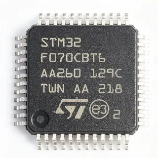
STM32L053C8T6 - Ultra-Low-Power ARM Cortex-M0+ MCU | STMicroelectronics
MPN: STM32L053C8T6 ✓ Active| Qty | Unit Price | Extended |
|---|---|---|
| 1 | $3.5 | $3.50 |
| 10 | $3.15 | $31.50 |
| 100 | $2.8 | $280.00 |
| 500 | $2.52 | $1,260.00 |
| 1,000 | $2.24 | $2,240.00 |
STM32L053C8T6 Overview
An ultra-low-power microcontroller (MCU) is a system-on-chip that integrates a processor core, memory, and peripherals, optimized for minimal energy consumption. The STM32L0 series is part of the STM32 family, which spans from entry-level Cortex-M0+ to high-performance Cortex-M7 cores. These MCUs are designed for battery-powered and energy-harvesting applications where power efficiency is critical, often featuring multiple low-power modes and dynamic voltage scaling.
Key features include multiple low-power modes (Sleep, Low-power Run, Low-power Sleep, Stop with RTC, Standby with RTC), a 12-bit ADC with hardware oversampling, a 12-bit DAC, two ultra-low-power comparators, and a USB 2.0 crystal-less device. The device also integrates a real-time clock (RTC) with calendar and alarm functions, and a true EEPROM emulation. The operating voltage range is 1.8V to 3.6V, with a temperature range of -40°C to +85°C.
The STM32L053C8T6 is built on ST's ultra-low-power technology, featuring a flexible power management that allows the core to run at 32 MHz while consuming only 84 µA/MHz in Run mode. The device supports a wide range of communication interfaces including I2C, SPI, USART, and LPUART, making it versatile for IoT and sensor applications. The integrated USB 2.0 interface supports both device and host modes, with a crystal-less design that reduces BOM cost.
Typical applications include IoT sensor nodes, wearable devices, smart home controllers, industrial sensors, and portable medical devices. The ultra-low-power consumption and rich analog peripherals make it ideal for battery-powered systems that require long operational life. The device also supports firmware updates via USB or UART bootloader, simplifying field maintenance.
When designing with this MCU, careful attention should be paid to the power supply decoupling and the selection of low-power modes to maximize battery life. The use of the internal 16 MHz HSI oscillator can reduce external component count, but for precise timing, an external crystal is recommended. The device's low-power modes require proper configuration of the RTC and wake-up sources to achieve optimal energy efficiency.
Drop-in alternatives for STM32L053C8T6 — same package, pin-to-pin compatible. Different-package parts requiring PCB rework are excluded.
Variants in this series
Same-series models that are drop-in compatible with STM32L053C8T6 (same form factor and footprint) — differing in ADC, Communication Interfaces, Comparators, Core, Operating Temperature.
Quick Comparison Tool — Select alternative parts for side-by-side comparison:
STM32L053C8T6TR
✅ Drop-In📋 Reference alternative (not in catalog)
STM32L053C6T6
✅ Drop-In📋 Reference alternative (not in catalog)
STM32L053C8T7
✅ Drop-In ⚠️ Specs Unverified📋 Reference alternative (not in catalog)
STM32L052C8T6
✅ Drop-In ⚠️ Specs Unverified📋 Reference alternative (not in catalog)
LPC824M201JHI33
✅ Drop-In ⚠️ Specs Unverified📋 Reference alternative (not in catalog)
STM32L053C8T6 Maximum Ratings & Electrical Characteristics
| Core | ARM Cortex-M0+ |
| Max Clock Speed | 32 MHz |
| Flash Memory | 64 KB |
| SRAM | 8 KB |
| Operating Voltage | 1.8 V to 3.6 V |
| Package | LQFP-48 |
| Operating Temperature | -40°C to +85°C |
| ADC | 12-bit, 16 channels |
| DAC | 12-bit, 1 channel |
| Comparators | 2 ultra-low-power |
| USB | 2.0 crystal-less device |
| Communication Interfaces | I2C, SPI, USART, LPUART |
| Low-Power Modes | Sleep, Low-power Run, Low-power Sleep, Stop, Standby |
| RTC | Calendar and alarm |
| RoHS Status | Compliant |
STM32L053C8T6 Pin Configuration
| Pin 1 | VBAT — Battery backup supply for RTC |
| Pin 2 | PC14 — GPIO / OSC32_IN |
| Pin 3 | PC15 — GPIO / OSC32_OUT |
| Pin 4 | OSC_IN — External clock input |
| Pin 5 | OSC_OUT — External clock output |
| Pin 6 | NRST — Reset (active low) |
| Pin 7 | VSSA — Analog ground |
| Pin 8 | VDDA — Analog power supply |
| Pin 9 | PA0 — GPIO / ADC_IN0 |
| Pin 10 | PA1 — GPIO / ADC_IN1 |
| Pin 11 | PA2 — GPIO / USART2_TX |
| Pin 12 | PA3 — GPIO / USART2_RX |
| Pin 13 | PA4 — GPIO / DAC_OUT1 |
| Pin 14 | PA5 — GPIO / SPI1_SCK |
| Pin 15 | PA6 — GPIO / SPI1_MISO |
| Pin 16 | PA7 — GPIO / SPI1_MOSI |
| Pin 17 | PB0 — GPIO / ADC_IN8 |
| Pin 18 | PB1 — GPIO / ADC_IN9 |
| Pin 19 | PB2 — GPIO / BOOT1 |
| Pin 20 | PB10 — GPIO / I2C2_SCL |
| Pin 21 | PB11 — GPIO / I2C2_SDA |
| Pin 22 | VSS — Ground |
| Pin 23 | VDD — Power supply |
| Pin 24 | PB12 — GPIO / SPI2_NSS |
| Pin 25 | PB13 — GPIO / SPI2_SCK |
| Pin 26 | PB14 — GPIO / SPI2_MISO |
| Pin 27 | PB15 — GPIO / SPI2_MOSI |
| Pin 28 | PA8 — GPIO / USB_DP |
| Pin 29 | PA9 — GPIO / USB_DM |
| Pin 30 | PA10 — GPIO / USART1_RX |
| Pin 31 | PA11 — GPIO / USART1_TX |
| Pin 32 | PA12 — GPIO / USART1_CTS |
| Pin 33 | PA13 — GPIO / SWDIO |
| Pin 34 | PA14 — GPIO / SWCLK |
| Pin 35 | PA15 — GPIO / SPI1_NSS |
| Pin 36 | PB3 — GPIO / SPI1_SCK |
| Pin 37 | PB4 — GPIO / SPI1_MISO |
| Pin 38 | PB5 — GPIO / SPI1_MOSI |
| Pin 39 | PB6 — GPIO / I2C1_SCL |
| Pin 40 | PB7 — GPIO / I2C1_SDA |
| Pin 41 | BOOT0 — Boot mode selection |
| Pin 42 | PB8 — GPIO / I2C1_SCL |
| Pin 43 | PB9 — GPIO / I2C1_SDA |
| Pin 44 | VSS — Ground |
| Pin 45 | VDD — Power supply |
| Pin 46 | PC13 — GPIO / RTC_TAMP1 |
| Pin 47 | PC14 — GPIO / OSC32_IN |
| Pin 48 | PC15 — GPIO / OSC32_OUT |
Typical Applications
STM32L053C8T6 is suitable for 6 applications: IoT Sensor Node, Wearable Health Monitor, Smart Home Controller, Industrial Sensor, Portable Medical Device, Energy Harvesting System.
IoT Sensor Node
The STM32L053C8T6 is ideal for IoT sensor nodes due to its ultra-low-power consumption and multiple low-power modes. In a typical application, the MCU wakes from Stop mode periodically to read sensors via I2C or SPI, process data, and transmit via a sub-GHz radio or BLE module. The 12-bit ADC with hardware oversampling enables precise sensor readings, while the LPUART allows low-power communication with external modules. The device's 84 µA/MHz Run mode current and 0.4 µA Standby mode with RTC ensure long battery life, making it perfect for battery-powered environmental monitoring, smart agriculture, and industrial sensing. Designers can leverage the RTC to schedule wake-ups, and the integrated USB can be used for configuration or data logging. The wide operating voltage range (1.8V-3.6V) allows direct connection to a lithium battery, simplifying power supply design.
Recommended
Wearable Health Monitor
The STM32L053C8T6 is well-suited for wearable health monitors such as fitness trackers and heart rate monitors. Its small LQFP-48 package and low power consumption enable compact, battery-powered designs. The MCU can interface with optical heart rate sensors (e.g., MAX30102) via I2C, process the data using the Cortex-M0+ core, and display results on a small OLED or transmit via BLE. The integrated DAC and comparators can be used for analog signal conditioning, while the RTC provides time-stamping for activity logs. The device's Stop mode with RTC (0.4 µA) allows the wearable to remain in a low-power state for extended periods, waking only to take measurements. The USB interface can be used for charging and data transfer, and the crystal-less USB reduces BOM cost. With a 3.7V Li-Po battery, the wide voltage range ensures stable operation, and the -40°C to +85°C temperature range covers all environmental conditions.
Recommended
Smart Home Controller
The STM32L053C8T6 serves as a central controller in smart home systems, managing lighting, HVAC, and security sensors. Its multiple communication interfaces (I2C, SPI, USART, LPUART) allow connection to various sensors and actuators, while the USB interface enables easy firmware updates and configuration. The device's low-power modes are crucial for always-on applications, where it can remain in Stop mode with RTC, waking to process commands from a central hub or smartphone. The 12-bit ADC can monitor analog sensors like thermistors or light sensors, and the DAC can generate analog control signals for dimmers. The RTC provides scheduling for automated routines, and the wide voltage range (1.8V-3.6V) allows operation from a 3.3V supply or battery backup. The STM32L053C8T6's robust peripheral set and low power make it an excellent choice for energy-efficient smart home devices.
Recommended
Industrial Sensor
The STM32L053C8T6 is designed for industrial sensor applications requiring low power and high reliability. It can interface with various industrial sensors (pressure, temperature, flow) via analog or digital interfaces, and process data for local display or transmission to a PLC. The 12-bit ADC with oversampling provides high-resolution measurements, while the comparators can be used for threshold detection. The device's wide temperature range (-40°C to +85°C) and robust design make it suitable for harsh environments. The LPUART allows low-power communication with industrial networks, and the RTC enables time-stamped data logging. The MCU's low-power modes are essential for battery-powered or energy-harvesting industrial sensors, where power consumption directly impacts maintenance intervals. The STM32L053C8T6's rich analog peripherals and communication options make it a versatile choice for industrial IoT.
Recommended
Portable Medical Device
The STM32L053C8T6 is suitable for portable medical devices such as glucose meters, pulse oximeters, and drug delivery systems. Its ultra-low-power consumption extends battery life, critical for patient convenience and safety. The device can interface with biosensors via I2C or SPI, process signals using the Cortex-M0+ core, and display results on an LCD or transmit via USB. The integrated DAC can generate analog waveforms for sensor excitation, and the comparators can detect alarm conditions. The RTC provides accurate time-stamping for medication schedules, and the wide voltage range (1.8V-3.6V) allows operation from a single coin cell. The STM32L053C8T6's small package and low power make it ideal for wearable or handheld medical devices, and its compliance with RoHS ensures environmental safety.
Recommended
Energy Harvesting System
The STM32L053C8T6 is optimized for energy harvesting applications, where power is scavenged from solar, thermal, or vibration sources. Its ultra-low-power consumption (84 µA/MHz) and multiple low-power modes allow the MCU to operate with minimal energy, making it ideal for self-powered sensors. The device can wake from Stop mode (0.4 µA) to take measurements, process data, and transmit via a low-power radio, then return to sleep. The wide voltage range (1.8V-3.6V) accommodates the variable output of energy harvesters, and the integrated ADC can monitor the harvester's output for maximum power point tracking. The RTC provides periodic wake-ups, and the LPUART enables low-power communication with external modules. The STM32L053C8T6's low power and rich peripherals make it a key component in sustainable IoT systems.
Recommended
Recommended Products Summary
Engineering reference data for STM32L053C8T6 — comparison, design guidance, and compliance information.
Selection Guide
Comparison with Alternatives
| Parameter | This Product | STM32L053C8T6TR | STM32L053C6T6 | STM32L053C8T7 | STM32L052C8T6 | LPC824M201JHI33 |
|---|---|---|---|---|---|---|
| Package | LQFP-48 | LQFP-48 - same | LQFP-48 - same | LQFP-48 - same | LQFP-48 - same | LQFP-48 - same |
| Brand | STMicroelectronics | STMicroelectronics | STMicroelectronics | STMicroelectronics | STMicroelectronics | NXP Semiconductors |
| Core | ARM Cortex-M0+ | ARM Cortex-M0+ | ARM Cortex-M0+ | ARM Cortex-M0+ | ARM Cortex-M0+ | ARM Cortex-M0+ |
| Max Clock Speed | 32 MHz | 32 MHz | 32 MHz | 32 MHz | 32 MHz | 30 MHz |
| Flash Memory | 64 KB | 64 KB | 32 KB | 64 KB | 64 KB | 32 KB |
| SRAM | 8 KB | 8 KB | 8 KB | 8 KB | 8 KB | 8 KB |
| USB | Yes (2.0 crystal-less) | Yes (2.0 crystal-less) | Yes (2.0 crystal-less) | Yes (2.0 crystal-less) | Yes (2.0 crystal-less) | No |
| DAC | Yes (12-bit) | Yes (12-bit) | Yes (12-bit) | Yes (12-bit) | No | No |
| Operating Voltage | 1.8V to 3.6V | 1.8V to 3.6V | 1.8V to 3.6V | 1.8V to 3.6V | 1.8V to 3.6V | 1.8V to 3.6V |
Key Differentiators
- Integrated USB 2.0 crystal-less device (vs LPC824M201JHI33)
- 12-bit DAC and comparators (vs STM32L052C8T6)
- 64 KB Flash memory (vs STM32L053C6T6)
Design Notes
Decouple the VDD and VDDA pins with 100 nF ceramic capacitors placed as close to the pins as possible. Additionally, use a 4.7 µF capacitor on VDDA for analog noise filtering. For the VBAT pin, connect a 100 nF capacitor to ground if using a backup battery. Proper decoupling ensures stable operation and reduces noise on the ADC and DAC.
For the crystal-less USB interface, ensure the USB_DP and USB_DM traces are routed with controlled impedance (90 ohms differential) and kept as short as possible. Place a 22 ohm series resistor on each line to reduce reflections. The LQFP-48 package has a 0.5 mm pitch, so use a fine-pitch PCB process and ensure adequate solder mask clearance.
When using the low-power modes, ensure that all unused GPIOs are configured to analog mode to avoid floating inputs that increase leakage current. Also, the RTC requires a valid clock source (LSE or LSI) to operate in Stop/Standby modes; if using the LSE, connect a 32.768 kHz crystal with 6 pF load capacitors. Failure to configure these can result in higher-than-expected power consumption.
Compliance Information
RoHS compliant per STMicroelectronics product page. Not AEC-Q100 qualified; for automotive, consider STM32L0 automotive variants.