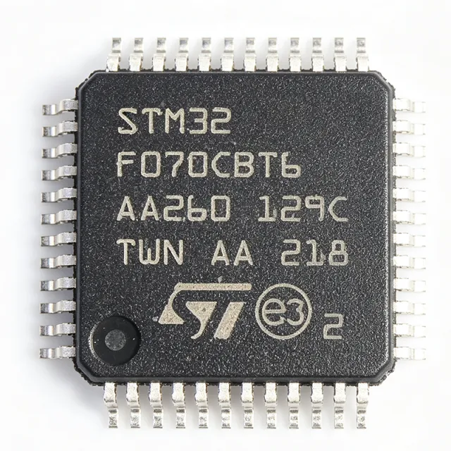
STM32F070CBT6 - ARM Cortex-M0 MCU 128KB Flash | STMicroelectronics
MPN: STM32F070CBT6 ✓ Active| Qty | Unit Price | Extended |
|---|---|---|
| 1 | $3.58 | $3.58 |
| 10 | $2.31 | $23.10 |
| 100 | $1.83 | $183.00 |
| 500 | $1.69 | $845.00 |
| 1,000 | $1.6 | $1,600.00 |
| 1,500 | $1.57 | $2,355.00 |
STM32F070CBT6 Overview
What is a microcontroller? A microcontroller (MCU) is a compact integrated circuit designed to govern a specific operation in an embedded system. It integrates a processor core, memory (Flash and SRAM), and programmable input/output peripherals on a single chip. The STM32F070CBT6 belongs to the STM32F0 series, which is part of the broader STM32 family of 32-bit ARM Cortex-M microcontrollers. This hierarchy places it within the ARM Cortex-M0 category, a low-power, entry-level core optimized for cost-sensitive applications.
Key features include a 12-bit ADC with up to 16 channels, multiple communication interfaces (I2C, SPI, USART), and a variety of timers including advanced-control timers. The device also includes a DMA controller, an RTC, and a CRC calculation unit. The LQFP-48 package provides a compact footprint suitable for space-constrained designs while offering sufficient I/O pins for peripheral connectivity.
The STM32F070CBT6 is built on a 32-bit ARM Cortex-M0 core with a Harvard architecture, achieving 1.25 DMIPS/MHz. It includes a nested vectored interrupt controller (NVIC) for efficient interrupt handling and supports both low-power modes (Sleep, Stop, Standby) to optimize energy consumption. The device is designed for a wide range of embedded applications requiring a balance of performance, power efficiency, and cost.
Typical applications include industrial control systems, consumer electronics, IoT devices, and home automation. Its rich peripheral set and low-power capabilities make it suitable for sensor interfacing, motor control, and communication protocols. The wide operating temperature range (-40°C to +85°C) ensures reliability in harsh environments.
When designing with this MCU, ensure proper decoupling of the power supply pins and consider the use of an external crystal for accurate timing. The device supports in-circuit programming and debugging via SWD, facilitating firmware development and updates.
This page synthesizes distributor pricing, drop-in alternatives, and practical design notes not found in the STMicroelectronics datasheet, providing engineers with a comprehensive resource for selection and implementation.
Drop-in alternatives for STM32F070CBT6 — same package, pin-to-pin compatible. Different-package parts requiring PCB rework are excluded.
Quick Comparison Tool — Select alternative parts for side-by-side comparison:
STM32F071CBT6
📋 Reference alternative (not in catalog)
STM32F072CBT6
📋 Reference alternative (not in catalog)
STM32F078CBT6
📋 Reference alternative (not in catalog)
STM32F070CBT6 Maximum Ratings & Electrical Characteristics
| Core | ARM Cortex-M0 |
| Core Frequency | 48 MHz |
| Flash Memory | 128 KB |
| SRAM | 16 KB |
| Supply Voltage | 2.4 V to 3.6 V |
| Package | LQFP-48 |
| Operating Temperature | -40°C to +85°C |
| ADC | 12-bit, 16 channels |
| Communication Interfaces | I2C, SPI, USART |
| Timers | Advanced-control, general-purpose, basic |
| DMA | Yes, 5 channels |
| RTC | Yes |
| CRC | Yes |
| Low-Power Modes | Sleep, Stop, Standby |
| Debug Interface | SWD |
| RoHS Status | Compliant |
STM32F070CBT6 Pin Configuration
| Pin 1 | VBAT — Battery backup supply for RTC |
| Pin 2 | PC13 — GPIO / RTC tamper |
| Pin 3 | PC14 — GPIO / OSC32_IN |
| Pin 4 | PC15 — GPIO / OSC32_OUT |
| Pin 5 | PF0 — GPIO / OSC_IN |
| Pin 6 | PF1 — GPIO / OSC_OUT |
| Pin 7 | NRST — Reset (active low) |
| Pin 8 | VSSA — Analog ground |
| Pin 9 | VDDA — Analog power supply |
| Pin 10 | PA0 — GPIO / ADC_IN0 / USART2_CTS |
| Pin 11 | PA1 — GPIO / ADC_IN1 / USART2_RTS |
| Pin 12 | PA2 — GPIO / ADC_IN2 / USART2_TX |
| Pin 13 | PA3 — GPIO / ADC_IN3 / USART2_RX |
| Pin 14 | PA4 — GPIO / ADC_IN4 / SPI1_NSS |
| Pin 15 | PA5 — GPIO / ADC_IN5 / SPI1_SCK |
| Pin 16 | PA6 — GPIO / ADC_IN6 / SPI1_MISO |
| Pin 17 | PA7 — GPIO / ADC_IN7 / SPI1_MOSI |
| Pin 18 | PB0 — GPIO / ADC_IN8 / TIM3_CH3 |
| Pin 19 | PB1 — GPIO / ADC_IN9 / TIM3_CH4 |
| Pin 20 | PB2 — GPIO / BOOT1 |
| Pin 21 | PB10 — GPIO / I2C2_SCL / USART3_TX |
| Pin 22 | PB11 — GPIO / I2C2_SDA / USART3_RX |
| Pin 23 | PB12 — GPIO / SPI2_NSS / I2C2_SMBA |
| Pin 24 | PB13 — GPIO / SPI2_SCK / USART3_CTS |
| Pin 25 | PB14 — GPIO / SPI2_MISO / USART3_RTS |
| Pin 26 | PB15 — GPIO / SPI2_MOSI |
| Pin 27 | PC6 — GPIO / TIM3_CH1 |
| Pin 28 | PC7 — GPIO / TIM3_CH2 |
| Pin 29 | PC8 — GPIO / TIM3_CH3 |
| Pin 30 | PC9 — GPIO / TIM3_CH4 |
| Pin 31 | PA8 — GPIO / MCO / TIM1_CH1 |
| Pin 32 | PA9 — GPIO / USART1_TX / TIM1_CH2 |
| Pin 33 | PA10 — GPIO / USART1_RX / TIM1_CH3 |
| Pin 34 | PA11 — GPIO / USART1_CTS / CAN_RX |
| Pin 35 | PA12 — GPIO / USART1_RTS / CAN_TX |
| Pin 36 | PA13 — GPIO / SWDIO |
| Pin 37 | VSS — Ground |
| Pin 38 | VDD — Power supply |
| Pin 39 | PA14 — GPIO / SWCLK |
| Pin 40 | PA15 — GPIO / TIM2_CH1 / SPI1_NSS |
| Pin 41 | PB3 — GPIO / TIM2_CH2 / SPI1_SCK |
| Pin 42 | PB4 — GPIO / TIM3_CH1 / SPI1_MISO |
| Pin 43 | PB5 — GPIO / TIM3_CH2 / SPI1_MOSI |
| Pin 44 | PB6 — GPIO / I2C1_SCL / TIM1_CH3 |
| Pin 45 | PB7 — GPIO / I2C1_SDA / TIM1_CH4 |
| Pin 46 | BOOT0 — Boot mode selection |
| Pin 47 | PB8 — GPIO / I2C1_SCL / CAN_RX |
| Pin 48 | PB9 — GPIO / I2C1_SDA / CAN_TX |
Typical Applications
STM32F070CBT6 is suitable for 6 applications: Industrial Control, Consumer Electronics, IoT Devices, Home Automation, Sensor Interfacing, Motor Control.
Industrial Control
The STM32F070CBT6 is well-suited for industrial control systems due to its robust peripheral set, including advanced timers for PWM generation, multiple USARTs for communication with PLCs, and a 12-bit ADC for sensor feedback. Its wide operating temperature range (-40°C to +85°C) ensures reliable operation in factory environments. In a typical motor control application, the MCU generates PWM signals to drive an H-bridge, reads current and position sensors via the ADC, and communicates status over RS-485. The 48 MHz Cortex-M0 core provides sufficient processing power for real-time control loops, while the DMA controller offloads data transfer to reduce CPU load. The low-power modes allow energy savings during idle periods, making it suitable for energy-efficient industrial equipment.
Recommended
Consumer Electronics
In consumer electronics, the STM32F070CBT6 provides a cost-effective solution for devices like smart home controllers, remote controls, and small appliances. Its low power consumption and multiple communication interfaces (I2C, SPI, USART) enable seamless integration with sensors, displays, and wireless modules. For example, in a smart thermostat, the MCU reads temperature and humidity sensors via I2C, controls a relay for heating/cooling, and communicates with a Wi-Fi module over UART. The 128KB Flash is ample for firmware implementing user interfaces and connectivity protocols. The LQFP-48 package is compact enough for sleek product designs, and the wide supply voltage range (2.4V-3.6V) allows direct battery operation. The device's low-power modes extend battery life in portable consumer devices.
Recommended
IoT Devices
The STM32F070CBT6 is an excellent choice for IoT edge nodes due to its balance of performance, power efficiency, and cost. It supports various communication protocols (UART, SPI, I2C) to interface with sensors and wireless transceivers. In a typical IoT sensor node, the MCU periodically wakes from Stop mode to read sensor data, process it, and transmit via a LoRa or BLE module. The 12-bit ADC with 16 channels allows multiple analog sensors to be connected directly. The DMA controller enables efficient data transfer without CPU intervention, reducing power consumption. The device's low-power Standby mode (1 µA typical) is critical for battery-powered deployments. With 128KB Flash, developers can implement robust firmware including over-the-air update capabilities.
Recommended
Home Automation
The STM32F070CBT6 is ideal for home automation hubs and smart devices. Its multiple UARTs and I2C interfaces allow connection to various sensors and actuators, while its low-power modes enable always-on operation with minimal energy consumption. In a smart lighting system, the MCU controls LED drivers via PWM, reads ambient light sensors, and communicates with a central hub over Zigbee or Wi-Fi. The 48 MHz core handles protocol stacks efficiently, and the 128KB Flash accommodates complex automation logic. The device's wide operating temperature range ensures reliable operation in residential environments. The LQFP-48 package is suitable for compact wall-mounted modules, and the SWD debug interface simplifies firmware development and updates.
Recommended
Sensor Interfacing
The STM32F070CBT6 excels in sensor interfacing applications due to its rich analog and digital peripherals. The 12-bit ADC with 16 channels can directly connect multiple analog sensors, while I2C and SPI interfaces support digital sensors. In a data acquisition system, the MCU samples temperature, pressure, and flow sensors, processes the data, and transmits it to a host via USART. The DMA controller allows continuous ADC sampling without CPU overhead, ensuring accurate data capture. The device's low-power modes are beneficial for remote sensor nodes powered by batteries. The 128KB Flash provides ample space for calibration tables and data logging. The wide supply voltage range accommodates various sensor supply requirements.
Recommended
Motor Control
The STM32F070CBT6 is well-suited for motor control applications, particularly for brushless DC (BLDC) and stepper motors. Its advanced-control timers can generate complementary PWM signals with dead-time insertion, essential for driving H-bridges. The 12-bit ADC enables precise current sensing, and the DMA controller facilitates high-speed data transfer. In a BLDC motor controller, the MCU reads Hall sensor inputs, generates six-step commutation signals, and regulates speed via PID control. The 48 MHz core provides sufficient computational power for real-time control loops. The device's robust timer architecture and fault handling features ensure safe operation. The LQFP-48 package is compact enough for integrated motor drivers, and the wide temperature range supports industrial motor applications.
Recommended
Recommended Products Summary
Engineering reference data for STM32F070CBT6 — comparison, design guidance, and compliance information.
Selection Guide
Comparison with Alternatives
| Parameter | This Product | STM32F071CBT6 | STM32F072CBT6 | STM32F078CBT6 |
|---|---|---|---|---|
| Package | LQFP-48 | LQFP-48 - same | LQFP-48 - same | LQFP-48 - same |
| Core Frequency | 48 MHz | 48 MHz | 48 MHz | 48 MHz |
| Flash Memory | 128 KB | 128 KB | 128 KB | 128 KB |
| SRAM | 16 KB | 16 KB | 16 KB | 16 KB |
| USB | Yes (full-speed device) | Yes (full-speed device) | Yes (full-speed device) | Yes (full-speed device) |
| CAN | No | No | Yes | Yes |
| DAC | No | Yes (12-bit) | Yes (12-bit) | Yes (12-bit) |
| Comparator | No | Yes | Yes | Yes |
| Price (1k) | $2.20 | $2.40 | $2.60 | $2.80 |
Key Differentiators
- USB full-speed device controller (vs STM32F030CBT6)
- Lower cost than F071/F072 (vs STM32F071CBT6)
- Pin-to-pin compatible with higher-feature siblings (vs STM32F072CBT6)
Design Notes
Decouple the VDD and VDDA pins with 100nF ceramic capacitors placed as close to the pins as possible. Additionally, add a 4.7uF bulk capacitor on the main VDD rail. For VDDA, use a ferrite bead in series to filter high-frequency noise, improving ADC accuracy.
For the LQFP-48 package, ensure proper solder paste stencil design with 0.5mm pitch. Use a 4-layer PCB with a solid ground plane beneath the MCU to reduce EMI and improve thermal performance. Route high-speed signals (SPI, USART) with controlled impedance if possible.
Do not leave unused GPIO pins floating; configure them as outputs or enable internal pull-ups/pull-downs to avoid excessive current consumption. Also, ensure the BOOT0 pin is properly pulled low for normal boot from Flash. For low-power modes, disable unused peripherals and clocks to achieve specified current consumption.
Compliance Information
RoHS and REACH compliant per STMicroelectronics. Not AEC-Q100 qualified; for automotive, consider STM32F0 series with AEC-Q100 option.


