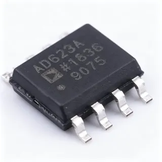
THS4031IDR - 100MHz Low-Noise Voltage Feedback Op-Amp | TI
MPN: THS4031IDR ✓ Active| Qty | Unit Price | Extended |
|---|---|---|
| 1 | $4.03 | $4.03 |
| 10 | $3.63 | $36.30 |
| 100 | $3.23 | $323.00 |
| 500 | $2.9 | $1,450.00 |
| 1,000 | $2.62 | $2,620.00 |
THS4031IDR Overview
A voltage-feedback amplifier (VFA) is a type of operational amplifier in which the feedback network senses voltage at the input pins, as opposed to a current-feedback amplifier (CFA) which senses current. Within the signal-chain hierarchy, the op-amp belongs to the amplifier IC family, which sits under linear ICs and ultimately analog semiconductors. Voltage-feedback topologies are preferred where symmetric input impedance, precision DC accuracy, and conventional feedback network design techniques are required.
Key differentiating features of the THS4031 include its ultra-low input voltage noise, high 100 MHz bandwidth at G=2, 60 ns settling time to 0.1%, and high output drive capability. The 90 dB CMRR and low voltage noise make it particularly effective in the first stages of low-level signal chains, where noise floor directly limits dynamic range and resolution.
Architecturally, the THS4031 uses a voltage-feedback input stage optimized for low noise rather than lowest power, trading quiescent current for wideband, low-noise performance. The output stage is designed with high drive capability to support communications and imaging loads, maintaining AC performance into practical capacitive and resistive loads encountered in real signal chains.
Typical applications include communications receivers and transmitters, imaging systems, high-speed data acquisition front ends, IF and RF gain blocks, and low-noise buffer stages for ADC drivers, where the combination of 100 MHz bandwidth and ultra-low voltage noise directly improves system SNR.
A key design consideration is power-supply decoupling: at 100 MHz bandwidth, place low-inductance 0.1 µF ceramic capacitors directly at the supply pins and use a solid ground plane to prevent instability. Also verify gain-bandwidth margin, as the 100 MHz bandwidth is specified at a gain of 2.
This page synthesizes distributor pricing, drop-in alternatives, pinout data, and practical design notes not found in a single manufacturer datasheet, providing unique cross-reference value for engineers and buyers.
Drop-in alternatives for THS4031IDR — same package, pin-to-pin compatible. Different-package parts requiring PCB rework are excluded.
Variants in this series
Same-series models that are drop-in compatible with THS4031IDR (same form factor and footprint) — differing in Package.
Quick Comparison Tool — Select alternative parts for side-by-side comparison:
THS4031CDR
✅ Drop-In✓ In Stock
$1.05 / Unit
View Datasheet →THS4031CD
✅ Drop-In📋 Reference alternative (not in catalog)
THS4031IDR Maximum Ratings & Electrical Characteristics
| Amplifier Type | Voltage Feedback |
| Number of Channels | 1 |
| Bandwidth at G=2 | 100 MHz |
| Unity-Gain Bandwidth | 275 MHz |
| Slew Rate | 100 V/us |
| CMRR | 90 dB |
| Settling Time (0.1%) | 60 ns |
| Operating Temperature Range | -40C to +85C |
| Package | 8-SOIC (0.154 in, 3.90 mm width) |
| Mounting Type | Surface Mount |
| Grade | Industrial (I temperature grade) |
| RoHS Status | Compliant |
THS4031IDR Pin Configuration
| Pin 1 | NC — Not connected |
| Pin 2 | IN- — Inverting input |
| Pin 3 | IN+ — Non-inverting input |
| Pin 4 | V- — Negative power supply |
| Pin 5 | NC — Not connected |
| Pin 6 | OUT — Amplifier output |
| Pin 7 | V+ — Positive power supply |
| Pin 8 | NC — Not connected |
Typical Applications
THS4031IDR is suitable for 6 applications: Communications Receiver Front End, Imaging System Signal Chain, High-Speed ADC Driver, IF and RF Gain Blocks, Low-Noise Buffer and Line Driver, Test and Measurement Instrumentation.
Communications Receiver Front End
The THS4031IDR fits communications receiver front ends because its ultra-low input voltage noise preserves the SNR of weak signals emerging from the mixer or filter stage, while the 100 MHz bandwidth at G=2 covers wide IF bands without gain roll-off. In a typical topology, the amplifier is placed after the channel filter as a fixed-gain (2x-10x) gain block driving an ADC or further IF stages, using the standard 8-SOIC pinout with 0.1 uF decoupling at pins 4 and 7. The 100 V/µs slew rate handles multi-volt-peak IF signals at tens of MHz without slew-induced distortion, and the 90 dB CMRR rejects ground-borne interference on differential-to-single-ended conversions. The trade-off versus lower-power op-amps is higher quiescent current, acceptable in line-powered communications equipment where dynamic range outranks battery life.
Recommended
Imaging System Signal Chain
The THS4031IDR is explicitly recommended by Texas Instruments for imaging applications, where the ultra-low voltage noise directly improves image SNR in CCD and CMOS sensor readout paths. The 100 MHz bandwidth at G=2 supports fast pixel-rate amplification and sample-and-hold buffering without settling artifacts, aided by the 60 ns settling time to 0.1%. A common topology places the amplifier as a programmable-gain stage or reset-noise-limited buffer between the column readout and the digitizer, with the 90 dB CMRR suppressing substrate and clock-feedthrough coupling on the ground reference. Compared with general-purpose high-speed amplifiers that trade noise for bandwidth, the THS4031's low-noise-optimized voltage-feedback architecture yields measurably lower read noise, which converts directly into higher effective imaging dynamic range at the system level.
Recommended
High-Speed ADC Driver
Driving high-speed pipeline and SAR analog-to-digital converters is a natural role for the THS4031IDR: the 100 MHz bandwidth provides ample loop gain at the ADC input frequencies, while the low input voltage noise keeps the amplifier's contribution below the converter's quantization and thermal noise floor, protecting the effective-number-of-bits (ENOB). The 100 V/µs slew rate tracks full-scale ADC input steps during acquisition windows, and the 60 ns settling to 0.1% supports sample rates in the tens of megasamples per second. Typically configured as a non-inverting gain stage or an active filter/driver between the sensor front end and the ADC input, the amplifier benefits from a series isolation resistor to manage capacitive charge kickback. The design trade-off is the noise-versus-power budget: lower-noise operation demands the THS4031's higher quiescent current compared with economy high-speed amplifiers.
Recommended
IF and RF Gain Blocks
As an IF/RF gain block, the THS4031IDR supplies broadband voltage gain with predictable phase behavior thanks to its voltage-feedback architecture, which engineers prefer for conventional resistor feedback networks and precise gain setting. The 100 MHz bandwidth at G=2 covers common IF frequencies in communications equipment, and the high output drive capability noted in the TI datasheet supports 50-ohm-terminated loads through a matching network. Gain is set with a resistor divider around the amplifier; keeping the feedback resistor moderate (hundreds of ohms) preserves bandwidth by minimizing the pole formed with input capacitance. The ultra-low voltage noise of the THS4031 is decisive here: in a receive chain, first-stage noise sets the system noise figure, so choosing this low-noise amplifier over a generic high-speed op-amp measurably improves receiver sensitivity and link margin.
Recommended
Low-Noise Buffer and Line Driver
The THS4031IDR serves as a low-noise unity-gain buffer for high-impedance or long interconnects, exploiting its unity-gain stability (275 MHz bandwidth) and high drive capability. Buffering a photodiode transimpedance stage output, a DAC output, or a test-point signal prevents downstream cable and load capacitance from loading the sensitive node, while the amplifier's own ultra-low voltage noise adds negligible noise to the preserved signal. In line-driving roles, the 100 V/µs slew rate supports fast edges over coaxial or twisted-pair runs, and the output stage drives terminated loads typical of instrumentation backplanes. Layout practice is critical: keep the feedback path short, decouple pins 4 and 7 with 0.1 uF ceramics directly at the SOIC-8 package, and use a solid ground plane to maintain stability across the full bandwidth.
Recommended
Test and Measurement Instrumentation
Bench and automated test equipment benefits from the THS4031IDR's combination of wide bandwidth, low noise, and predictable voltage-feedback gain accuracy. Typical roles include vertical-channel preamplifiers in digitizing instruments, active probes, signal-conditioning front ends, and reference-signal buffers, where the 100 MHz bandwidth and 60 ns settling time preserve waveform fidelity across the instrument's passband. The 90 dB CMRR protects differential measurements from ground-loop interference between the device under test and the instrument chassis, and the industrial -40C to +85C rating supports equipment deployed in unconditioned environments. Compared with faster current-feedback amplifiers, the THS4031's voltage-feedback topology allows precision gain-set resistors without bandwidth sensitivity to feedback value - a practical advantage when calibrating instrument gain in production.
Recommended
Recommended Products Summary
Engineering reference data for THS4031IDR — comparison, design guidance, and compliance information.
Selection Guide
Comparison with Alternatives
| Parameter | This Product | THS4031CDR | THS4031CD |
|---|---|---|---|
| Package | 8-SOIC (D) | 8-SOIC (D) - same | 8-SOIC (D) - same |
| Brand | Texas Instruments | Texas Instruments | Texas Instruments |
| Bandwidth (G=2) | 100 MHz | 100 MHz | 100 MHz |
| Slew Rate | 100 V/us | 100 V/us | 100 V/us |
| CMRR | 90 dB | 90 dB | 90 dB |
| Operating Temperature | -40C to +85C | 0C to +70C | 0C to +70C |
| Settling Time (0.1%) | 60 ns | 60 ns | 60 ns |
| Packaging | Tape & Reel (R suffix) | Tape & Reel | Tube |
Key Differentiators
- Ultra-low input voltage noise optimized architecture (vs Generic 100 MHz high-speed op-amps)
- Industrial temperature grade availability (vs THS4031CDR)
- Voltage-feedback topology for precision gain setting (vs Current-feedback alternatives at similar bandwidth)
Design Notes
At 100 MHz bandwidth, decoupling quality determines stability. Place 0.1 uF low-ESL ceramic capacitors within 2-3 mm of pins 4 (V-) and 7 (V+) of the SOIC-8, with vias directly to a solid ground plane. Avoid long thin supply traces, which add inductance and create high-frequency resonance. The NC pins (1, 5, 8) can be left floating or tied to ground pour for symmetry; keep the feedback resistor path as short as possible to limit parasitic capacitance at the inverting input.
The 100 MHz bandwidth is specified at a gain of 2; verify loop gain margin at your actual closed-loop gain. Use moderate feedback resistor values (hundreds of ohms) - too large a value forms a pole with input capacitance that erodes phase margin, while too small a value loads the output stage. For unity-gain buffering, the part is stable by design (275 MHz unity-gain bandwidth), but a small feedback capacitor may be added to flatten peaking with capacitive loads.
Do not substitute the commercial-grade THS4031CDR into industrial designs: its 0C to +70C rating will cause out-of-spec operation below freezing, whereas the THS4031IDR is rated -40C to +85C. Confirm supply voltage limits in the TI datasheet before applying rails, as high-speed amplifiers often have absolute maximum ratings well below general-purpose parts. Estimated: power dissipation equals (V+ - VOUT)*IOUT plus quiescent power; check SOIC-8 thermal limits for high-current output applications.
Compliance Information
RoHS compliance indicated in ETEI comparison data and standard TI D-prefix (RoHS-compliant SOIC) suffix usage. REACH and halogen-free status not stated in provided data - verify on TI.com quality pages.