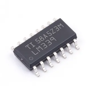
TLV2454ID - 23µA Quad RRIO Op Amp | Texas Instruments
MPN: TLV2454ID ✓ ActiveTLV2454ID Overview
An operational amplifier is an analog signal-processing IC that amplifies the voltage difference between its inverting and non-inverting inputs. The rail-to-rail input stage accepts signals extending close to the positive and negative supply rails, while the rail-to-rail output stage can swing close to those rails under suitable load conditions. Within the power-management hierarchy, the TLV2454ID is a low-voltage, micropower amplifier suitable for battery-operated equipment where four precision amplifier channels are needed without the higher current demand of general-purpose quad op amps.
The TLV2454ID combines 220 kHz gain-bandwidth product with approximately 23 µA quiescent current per amplifier. Its typical input offset voltage is 20 µV, input bias current is 4.5 nA, and input voltage noise is 49 nV/√Hz at 100 Hz. The device also provides 70 dB common-mode rejection, 110 V/ms slew rate, and output drive capability of 10 mA. These characteristics make it useful for precision dc signal conditioning, low-level sensor amplification, and buffered analog measurement nodes.
The quad architecture implements four independent amplifiers in one 14-pin SOIC, reducing board area compared with discrete single or dual amplifier packages. Rail-to-rail input common-mode range and rail-to-rail output capability improve signal-chain flexibility on 2.7 V to 6 V supplies. Because the operating current is specified per channel, designers should calculate the total static demand from four channels and include the load current of the application when assessing battery life.
Typical uses include portable medical monitoring, low-power sensor acquisition, industrial current measurement, battery-powered test equipment, and general-purpose analog buffering. In sensor circuits, the low offset voltage and low bias current can minimize errors from slow-changing sensor signals. For bidirectional current sensing, the low-noise input stage supports small shunt voltages, while the 10 mA output-drive rating provides useful capability for driving subsequent analog stages.
Choose stable, low-ESR bypass capacitors and route each supply connection to its decoupling capacitor through low-impedance PCB traces. Confirm output swing, input common-mode limits, capacitive-load stability, and total channel current under worst-case conditions. Avoid using the output as a high-current buffer and verify that the selected gain and feedback network remain stable at the intended operating voltage.
This product page combines the TLV2454ID's principal electrical characteristics with same-family replacement guidance and practical PCB guidance. It helps engineers distinguish exact drop-in options from higher-speed or otherwise different amplifier families before committing a 14-pin SOIC footprint to a low-power design.
Drop-in alternatives for TLV2454ID — same package, pin-to-pin compatible. Different-package parts requiring PCB rework are excluded.
TLV2454AIDG4
✅ Drop-In📋 Reference alternative (not in catalog)
TLV2455IDR
✅ Drop-In📋 Reference alternative (not in catalog)
TLV2464AID
✅ Drop-In📋 Reference alternative (not in catalog)
TLV2454ID Maximum Ratings & Electrical Characteristics
| Number of Amplifiers | 4 channels |
| Supply Voltage Range | 2.7 V to 6 V |
| Quiescent Current per Channel | 23 µA |
| Gain-Bandwidth Product | 220 kHz |
| Input Offset Voltage | 20 µV typical |
| Input Bias Current | 4.5 nA typical |
| Input Voltage Noise | 49 nV/√Hz at 100 Hz |
| Input Offset Voltage Drift | 300 nV/°C |
| Common-Mode Rejection | 70 dB |
| Slew Rate | 110 V/ms |
| Output Drive Capability | 10 mA |
| Input Common-Mode Range | -3 V to -1.35 V and 1.35 V to 3 V |
| Operating Temperature Range | -40°C to +125°C |
| Package | SOIC-14 |
| Mounting Type | Surface mount |
| RoHS Status | Compliant |
TLV2454ID Pin Configuration
| Pin 1 | OUTA — Amplifier A output |
| Pin 2 | INA- — Amplifier A inverting input |
| Pin 3 | INA+ — Amplifier A non-inverting input |
| Pin 4 | V+ — Positive supply voltage |
| Pin 5 | INB+ — Amplifier B non-inverting input |
| Pin 6 | INB- — Amplifier B inverting input |
| Pin 7 | OUTB — Amplifier B output |
| Pin 8 | OUTC — Amplifier C output |
| Pin 9 | INC- — Amplifier C inverting input |
| Pin 10 | INC+ — Amplifier C non-inverting input |
| Pin 11 | V- — Negative supply voltage |
| Pin 12 | IND+ — Amplifier D non-inverting input |
| Pin 13 | IND- — Amplifier D inverting input |
| Pin 14 | OUTD — Amplifier D output |
Typical Applications
TLV2454ID is suitable for 6 applications: Portable Medical Sensor Acquisition, Battery-Powered Industrial Sensing, Precision Current Measurement, Portable Test and Measurement, Low-Voltage Signal Conditioning, Battery Charging and Power Monitoring.
Portable Medical Sensor Acquisition
The TLV2454ID fits portable medical-sensor front ends that operate from a 2.7 V to 6 V rail and require several low-power analog channels. Its 23 µA quiescent current per channel limits static battery demand, while 4.5 nA typical input bias current helps preserve high-impedance sensor signals. Four rail-to-rail input/output amplifiers can condition pressure, temperature, or bio-sensor nodes without using four separate packages. The 220 kHz gain-bandwidth product is appropriate for low-frequency physiological signals rather than wideband waveform reconstruction.
Recommended
Battery-Powered Industrial Sensing
The TLV2454ID supports battery-powered industrial sensor nodes where several low-level signals must be amplified without a high quiescent-power penalty. The 23 µA current per channel is useful when four channels operate continuously, and the 20 µV typical input offset helps preserve accuracy from slow-changing bridge or resistive sensors. Rail-to-rail input operation allows more of a 2.7 V to 6 V supply range to be used. The 110 V/ms slew rate supports signal changes that are faster than static dc measurements but do not require high bandwidth.
Recommended
Precision Current Measurement
The TLV2454ID is suitable for amplifying the small differential voltage produced by a shunt in precision current-measurement circuits. Its 4.5 nA typical input bias current and 70 dB common-mode rejection help reject errors from common-mode voltage and source impedance, while 49 nV/√Hz input noise at 100 Hz supports low-level signal conditioning. Four channels can monitor several loads or provide differential and common configurations. The 10 mA output-drive rating is adequate for intermediate analog stages but not for low-ohmic direct loads.
Recommended
Portable Test and Measurement
The TLV2454ID is useful in handheld test and measurement equipment requiring four general-purpose amplifier channels in a compact 14-pin SOIC. It can buffer sensor outputs, amplify intermediate signals, and provide gain stages for low-frequency waveforms while drawing only 23 µA per channel. The 2.7 V minimum supply supports single-cell-derived 3 V systems, and rail-to-rail operation improves usable signal range. Instrument designers should still account for the 220 kHz bandwidth limit when evaluating step response and precision near the upper operating frequency.
Recommended
Low-Voltage Signal Conditioning
The TLV2454ID is appropriate for general low-voltage signal conditioning between sensors, converters, and data-conversion stages. Four rail-to-rail amplifiers can amplify, level-shift, or buffer channels within a 2.7 V to 6 V system. Its low 23 µA per-channel current reduces overhead in continuously powered equipment, while the 110 V/ms slew rate and 10 mA output drive provide useful performance for moderate-speed analog signals. Feedback-network design remains important because each channel must remain stable at the selected gain and supply voltage.
Recommended
Battery Charging and Power Monitoring
The TLV2454ID can support low-current battery monitoring and power-management signal chains where a 2.7 V to 6 V rail is available. Its four channels may monitor temperature, current, voltage thresholds, or charger status while keeping each channel's quiescent demand at 23 µA. Rail-to-rail inputs and outputs improve signal utilization in compact power systems, and the 14-pin SOIC reduces footprint compared with four single amplifiers. Designers should verify the actual output swing under load and confirm that transient currents from the charger do not violate output-drive or supply limits.
Recommended
Recommended Products Summary
Engineering reference data for TLV2454ID — comparison, design guidance, and compliance information.
Selection Guide
Comparison with Alternatives
| Parameter | This Product | TLV2454AIDG4 | TLV2455IDR | TLV2464AID |
|---|---|---|---|---|
| Brand | Texas Instruments | Texas Instruments | Texas Instruments | Texas Instruments |
| Package | SOIC-14 | SOIC-14 - same | SOIC-14 - same | SOIC-14 - same |
| Number of Amplifiers | 4 channels | 4 channels | 4 channels | 4 channels |
| Quiescent Current per Channel | 23 µA | 23 µA | 23 µA | 200 µA |
| Gain-Bandwidth Product | 220 kHz | 220 kHz | 1 MHz | 10 MHz |
Key Differentiators
- Lower quiescent-current family option (vs TLV2464AID)
- Same-family replacement preserves core performance (vs TLV2454AIDG4)
- Higher bandwidth option remains package-compatible (vs TLV2455IDR)
Design Notes
Place the V+ and V- bypass capacitors close to their respective SOIC-14 supply pins, with short ground returns and minimal loop area. Use a common ground plane unless the circuit requires an isolated return. Keep sensitive input nodes away from supply and output routing, especially when the TLV2454ID amplifies microvolt-level signals; high-impedance traces can otherwise couple output and switching noise back into the input.
Estimated: four channels operating at the specified 23 µA quiescent current draw 92 µA before load current. Add output current, bias-network current, and regulator losses to determine total supply demand. For a 3 V system, the four-channel static amplifier power is approximately 0.28 mW. These values are design estimates based on the 3 V rail and 23 µA per-channel specification, not maximum-current or operating-condition guarantees.
Do not interpret rail-to-rail input as unlimited input range. At the extremes of the 2.7 V to 6 V supply range, the input common-mode behavior changes, and the listed -3 V to -1.35 V and 1.35 V to 3 V ranges require careful interpretation against the selected supply. Likewise, confirm the 10 mA output-drive capability before driving a load and verify capacitive-load stability for the chosen gain and feedback network.
Compliance Information
The component listing identifies the TLV2454ID as RoHS compliant. No explicit REACH, lead-free, halogen-free, conflict-minerals, or automotive-qualification statement was identified.