CIs Amplificadores
Produtos (563)

OPA2277UA - 10µV Dual Precision Op Amp | Texas Instruments
The Texas Instruments OPA2277UA is a dual-channel, high-precision, low-power operational amplifier supplied in an 8-pin SOIC (D-package) that replaces the legacy OP-177 with substantially better noise, wider output swing, twice the speed, and half the quiescent current. The OPA2277UA delivers an ultra-low input offset voltage of 10 µV (max), an ultra-low offset drift of ±0.1 µV/°C, an open-loop gain of 134 dB, common-mode rejection of 140 dB, and high power-supply rejection while drawing only 800 µA of quiescent current per channel. It is specified for ±2 V to ±18 V supplies, swings to within 1 V of each rail on a ±15 V supply, and operates across the -40°C to +125°C industrial temperature range. Background knowledge: A precision op-amp (operational amplifier) is a high-gain DC-coupled analog building block whose input offset voltage, offset drift, bias current, and noise are engineered to far tighter limits than those of a general-purpose op-amp. Within the signal-chain hierarchy, the OPA2277 sits in the "precision" tier between general-purpose amplifiers (e.g. OPA234) and zero-dr chopper-stabilized amplifiers (e.g. OPA2188), drawing meaningfully lower bias current than old bipolar parts (e.g. OP-27) while delivering lower voltage noise than early CMOS parts (e.g. TLC2277). It is functionally a "dual, improved OP-177" intended for bridge amplifiers, strain gauges, thermocouple conditioning, and precision active filters where µV-level DC accuracy must be preserved across -40°C to +125°C. Architecturally, the OPA2277 uses a bipolar transistor input stage with laser-trimmed thin-film resistors, a complementary bipolar output stage capable of driving 2 kΩ loads, and internal compensation that removes the need for an external compensation capacitor. The result is a stable unity-gain device that does not oscillate when used as a buffer, with a gain-bandwidth product of 1 MHz and a 2 V/µs slew rate that supports audio-bandwidth signal conditioning, 16-bit ADC input buffers, and reference-voltage buffers. Typical applications include precision weighing scales and load-cell signal chains (where 10 µV Vos preserves mV-level bridge outputs), industrial process-control 4-20 mA loop transmitters, medical instrumentation front-ends, precision active filters, multi-channel data-acquisition multiplexed front ends, and reference-voltage buffers for 16-bit and 18-bit ADCs. The wide supply range also allows use in ±15 V legacy industrial backplanes. A practical design consideration: although the OPA2277 is unity-gain stable, its 1 MHz GBW means it is best used for DC-accurate low-frequency applications (sub-100 kHz). For higher-bandwidth precision needs, the OPA2227 (same package, 13 MHz GBW) or OPA2156 (pin-compatible, lower noise) are better choices; choose this part when DC accuracy and price dominate over bandwidth. This page synthesizes distributor stock and pricing, AEO-optimized FAQ, and drop-in alternatives that complement the manufacturer datasheet.
OPA2335AIDR - Dual Zero-Drift 5uV 2MHz Op Amp | TI
The Texas Instruments OPA2335AIDR is a dual-channel, zero-drift CMOS operational amplifier (op-amp) in an 8-pin SOIC package, delivering 5 uV (max) offset voltage and 0.05 uV/°C (max) drift over temperature. It provides a 2 MHz gain-bandwidth product, rail-to-rail output swing, and operates from a single 2.7V to 5.5V supply with a typical quiescent current of 285 uA per channel. The "D" suffix indicates tape-and-reel packaging and the "R" suffix designates the SOIC-8 (D) small-outline package. A zero-drift amplifier (also called auto-zero or chopper-stabilized op-amp) is a precision amplifier topology that continuously samples and corrects its own input offset voltage, virtually eliminating the 1/f noise corner and drift over time and temperature. Within the broader taxonomy, zero-drift op-amps sit beneath precision amplifiers and instrumentation amplifiers, above general-purpose CMOS op-amps; they are critical in any signal chain where DC accuracy over temperature matters more than absolute bandwidth. Key features include 5 uV maximum offset voltage, 0.05 uV/°C maximum drift, single-supply operation from 2.7V to 5.5V, 2 MHz GBW, rail-to-rail output, 285 uA quiescent current per channel, and a miniature SOIC-8 footprint. The chopper-stabilized topology eliminates the 1/f noise corner, producing flat noise spectral density down to DC - a feature classical CMOS op-amps cannot match. The OPA2335 uses TI's auto-zeroing architecture that combines a main amplifier with a nulling amplifier. The nulling amplifier periodically samples the offset and applies a correction, yielding near-zero long-term drift. This makes the device particularly well suited for high-gain DC stages, sensor signal conditioning, and 16-bit-plus precision analog-to-digital converter (ADC) front ends where offset drift directly translates to system error. Typical applications include transducer signal conditioning, electronic weighing scales (electronic balances), medical instrumentation such as ECG and patient monitors, temperature measurement (RTD and thermocouple amplifiers), and precision analog front-ends for industrial process control. In each case the OPA2335's near-zero drift preserves calibration accuracy over the full operating temperature range. When designing with the OPA2335, observe the standard zero-drift caveat: the auto-zero clock produces small intermodulation artifacts in the kHz region that can alias into audio-frequency bands - a small post-filter or careful GBW selection mitigates this. Decouple each supply pin with a 0.1 uF ceramic capacitor placed within a few millimeters of the IC. This page synthesizes distributor pricing, drop-in compatible alternatives in the SOIC-8 footprint, parametric comparisons with same-package peers, and practical design notes not found in the manufacturer datasheet alone.
OPA2350UA/2K5 - Dual 38MHz Rail-to-Rail Op Amp | Texas Instruments
The Texas Instruments OPA2350UA/2K5 is a dual, single-supply, rail-to-rail CMOS operational amplifier featuring 38 MHz gain-bandwidth, 22 V/µs slew rate, and 5 nV/√Hz input-noise density in an 8-pin SOIC package. The two amplifiers share a common package while providing independent input, output, and supply connections for dual-channel signal conditioning. According to the verified TI product information, the device is optimized for low-voltage operation and is intended for high-speed, low-noise analog signal chains. What is a rail-to-rail operational amplifier? A rail-to-rail input amplifier accepts input voltages across nearly the entire supply range, while a rail-to-rail output amplifier can swing its output close to the positive and negative supply rails. The OPA2350 combines these capabilities with high-speed small-signal performance and low noise. In the broader electronics hierarchy, it is a CMOS operational amplifier within the linear-amplifier and signal-conditioning categories. The verified feature set emphasizes 38 MHz bandwidth, 22 V/µs slew rate, 5 nV/√Hz noise density, and rail-to-rail output operation within 10 mV. These figures make the device suitable for applications that require fast settling or low-noise amplification, including sampling analog-to-digital converter input stages. The family is also identified for cell-phone power-amplifier control loops and 75-ohm video-processing drive applications. OPA2350UA/2K5 is specified as a dual amplifier in an 8-pin SOIC (D) package. The verified operating-temperature entry is -40°C to +85°C for this ordering variant. Rail-to-rail input and output behavior is particularly useful in low-voltage systems where the usable signal range is close to the supply limits and where conventional non-rail-to-rail amplifiers would clip or compress the signal. Typical circuit roles include ADC signal conditioning, video-buffer or drive functions, control-loop amplification, and other high-speed analog front-end stages. The dual configuration can process two related channels, such as a differential or paired sensor signal, without requiring two separate packages. Designers should verify the supply voltage, load, stability, and output-swing requirements against the complete manufacturer datasheet before finalizing the analog path. A key design consideration is to preserve the amplifier’s high-speed behavior by minimizing parasitic capacitance and using short, well-routed traces. Decoupling capacitors should be placed close to the supply pins, and sensitive input nodes should avoid proximity to switching nodes and high-current return paths. Because the verified data does not provide a complete electrical parameter table for every operating condition, consult the TI datasheet for precise limit values. This page combines verified TI product facts, distributor availability references, practical design guidance, and structured comparison information. It is intended to help engineers identify whether the OPA2350UA/2K5 matches the required bandwidth, slew-rate, noise, supply, and package constraints.

OPA2375 - Dual 10MHz Low-Noise CMOS Op Amp | Texas Instruments
The Texas Instruments OPA2375 is a dual-channel, general-purpose CMOS operational amplifier delivering a 10 MHz gain-bandwidth product, an ultra-low broadband noise of 4.6 nV/rtHz (per-channel typical at 10 kHz), and a maximum input offset voltage of 500 uV. It operates from a single 2.2V to 5.5V supply with rail-to-rail output (RRO) and is supplied in an 8-pin TSSOP package (OPA2375IPWR). An operational amplifier is a high-gain voltage amplifier with differential inputs, foundational to the analog signal-chain hierarchy: op amp -> amplifier IC -> analog front end -> semiconductor. The OPA2375 belongs to the OPAx375 family, which includes the single-channel OPA375 and quad-channel OPA4375, all sharing the same core CMOS silicon and specifications. Key features include low broadband noise (3.5 nV/rtHz family figure, 4.6 nV/rtHz for the dual at specified conditions), a wide 10 MHz bandwidth suited to active filters and transimpedance stages, rail-to-rail output swing that maximizes dynamic range on 3.3V and 5V rails, and low offset of 500 uV maximum that reduces DC error without needing auto-zero calibration. CMOS construction gives low input bias current, important for high-impedance sources. Architecturally, the OPA2375 uses a CMOS input pair with a precision trim at wafer test, achieving a strong noise-bandwidth-offset balance that makes the OPAx375 family attractive for precision applications requiring good AC performance at low cost. Unity-gain stability and rail-to-rail output simplify buffer and driver designs. Typical applications include sensor signal conditioning, active anti-aliasing filters ahead of precision ADCs, transimpedance amplifiers for photodiodes, and medical or portable instrumentation where low noise and wide bandwidth on a single 5V rail are required. The dual channel halves board area versus two singles. Design consideration: keep source impedance below approximately 1 kOhm to preserve the nV-level noise floor, and decouple each supply pin with 0.1 uF ceramics placed close to the device.

OPA2375IDDFR - Dual 10MHz 4.6nV Op Amp, TSOT-23-8 | TI
The Texas Instruments OPA2375IDDFR is a dual-channel, 10-MHz, low-noise (4.6 nV per root-hertz) rail-to-rail output (RRO) CMOS operational amplifier operating from a 2.2 V to 5.5 V single supply, housed in an 8-pin TSOT-23-8 (DDF) surface-mount package. An operational amplifier (op amp) is a high-gain voltage amplifier with differential inputs, and it sits at the core of the analog signal chain hierarchy: op amp -> amplifier IC -> analog integrated circuit -> signal-conditioning subsystem. Within this hierarchy, low-noise precision CMOS amplifiers such as the OPA2375 bridge the gap between general-purpose and precision instrumentation amplifiers, conditioning sensor and transducer signals before analog-to-digital conversion. Key features of the OPA2375IDDFR include a 10 MHz gain-bandwidth, an input-referred broadband noise of only 4.6 nV per root-hertz, a maximum input offset voltage of 500 uV, and rail-to-rail output swing that maximizes dynamic range on low-voltage rails. The CMOS input provides high input impedance and low bias current, important for high-impedance sensor interfaces. Architecturally, the OPAx375 family (OPA375 single, OPA2375 dual, OPA4375 quad) uses a CMOS input stage with a rail-to-rail output stage (RRO). This combination delivers wide bandwidth and low noise simultaneously, a pairing usually traded off against each other, and the low offset of 500 uV maximum keeps DC accuracy acceptable in precision signal chains without system-level trimming. Typical applications include sensor signal conditioning for pressure and temperature transducers, active filter stages ahead of precision ADCs, and transimpedance or buffer amplification in portable and battery-powered instrumentation where the 5.5 V maximum supply and small TSOT-23-8 footprint save board area. Design consideration: the OPA2375 provides rail-to-rail output only (RRO), not rail-to-rail input. Keep the common-mode input range within the specified limits, typically about 1.5 V from either rail, or verify linearity in your operating region before committing the layout. This page synthesizes distributor pricing from DigiKey, Mouser, LCSC and Octopart, drop-in alternative analysis, and practical design notes not found in the manufacturer datasheet, giving engineers a single citable reference for the OPA2375IDDFR.
OPA2375IDGKR - Dual 10MHz Rail-to-Rail Op Amp | TI
The Texas Instruments OPA2375IDGKR is a dual-channel, 10 MHz CMOS operational amplifier with rail-to-rail output (RRO), 4.6 nV/√Hz low broadband noise, and 500 µV maximum input offset voltage, housed in an 8-pin VSSOP (DGK) surface-mount package. An operational amplifier (op amp) is a high-gain voltage amplifier with differential inputs that, when combined with external feedback networks, performs amplification, filtering, buffering, and signal conditioning. Within the signal-chain hierarchy, the op amp sits between sensors and data converters: it is a core analog building block of the amplifiers and buffer amplifiers category, and the OPA2375 belongs to the OPAx375 general-purpose CMOS family that also includes the single OPA375 and quad OPA4375. Key differentiating features include the extremely low 4.6 nV/√Hz broadband noise figure, a wide 10 MHz gain-bandwidth, a fast 4.6 V/µs slew rate (per distributor package data), and rail-to-rail output swing that maximizes dynamic range in low-voltage systems. The maximum 500 µV offset and only 3 pA input bias current make the device suitable for high-impedance sources. Technically, the OPA2375 uses a CMOS input architecture with a rail-to-rail output stage, which allows output swings to within millivolts of either supply rail. This CMOS design delivers low noise without the input bias currents of bipolar alternatives, and the low-voltage 5.5 V maximum supply rating aligns the amplifier directly with 3.3 V and 5 V single-supply systems, ADC drivers, and portable designs. Typical applications include sensor signal conditioning and transimpedance amplification for photodiodes (enabled by the 3 pA bias current), active anti-alias filters ahead of SAR and delta-sigma ADCs, and general-purpose precision amplification in industrial and portable instrumentation. The dual channel integration saves board area versus two single amplifiers. When designing, account for supply decoupling with 0.1 µF ceramics close to each V+ pin, and verify that closed-loop gain and load capacitance keep the amplifier comfortably within its 10 MHz bandwidth and phase-margin limits for stability. This page synthesizes distributor pricing, drop-in alternatives, design notes, and pin-to-pin replacement guidance not found in the manufacturer datasheet alone.

OPA2375IDSGR - 10MHz Dual CMOS Op Amp RRO | Texas Instruments
The Texas Instruments OPA2375IDSGR is a dual-channel, 10-MHz, low-noise (3.5 nV/sqrtHz broadband, 4.6 nV/sqrtHz per the TI product page) CMOS operational amplifier with rail-to-rail output (RRO), supplied in an 8-pin WSON (DSG) 2x2 mm surface-mount package. It operates from a supply up to 5.5 V and draws only 990 uA per channel. An operational amplifier (op amp) is a high-gain differential voltage amplifier that forms the core building block of analog signal conditioning. Within the power-management and signal-chain hierarchy, op amps sit in the amplifier IC category alongside instrumentation amplifiers and buffer amplifiers, conditioning sensor outputs, filtering signals, and driving ADC inputs. The OPA2375 belongs to the OPAx375 family, which includes the single OPA375, dual OPA2375, and quad OPA4375. Key differentiating features include an extremely low broadband noise figure of 3.5 nV/sqrtHz, a maximum input offset voltage of only 500 uV, very low distortion (THD+N of 0.00015%), a 10 MHz gain bandwidth, and unity-gain stability. These combine to deliver precision performance rarely found in general-purpose CMOS op amps at this quiescent current level. Technically, the OPA2375 uses a CMOS input architecture that achieves near-zero input bias current together with low 1/f noise, while the rail-to-rail output stage maximizes dynamic range on low single-supply rails such as 3.3 V and 5 V. The output swing within millivolts of either rail allows the full ADC input range to be exploited in compact battery-powered designs. Typical applications include sensor signal conditioning for battery-powered devices, active filter and transimpedance stages in portable medical instruments, and driving precision successive-approximation ADCs such as the ADS131M08 in industrial data-acquisition systems. Design consideration: the 2x2 mm WSON (DSG) package has a small thermal pad and fine 0.5 mm pitch, so inspect the PCB land pattern carefully and use a ground plane for heat spreading and stable high-frequency performance. Input and output RC filtering is recommended when driving heavily capacitive loads. This page synthesizes distributor availability, drop-in alternative analysis, pinout details, and practical design notes not consolidated in the manufacturer datasheet, with pricing as of 2026-09-03.

OPA2375IPWR - 10MHz 4.6nV/√Hz Dual CMOS Op Amp | TI
The Texas Instruments OPA2375IPWR is a dual-channel general-purpose CMOS operational amplifier delivering a 10 MHz gain-bandwidth product, an ultra-low 4.6 nV/√Hz broadband noise figure, and a maximum 500 μV input offset voltage, housed in an 8-pin TSSOP (PW) surface-mount package with rail-to-rail output (RRO). An operational amplifier (op amp) is a high-gain differential-input voltage amplifier that forms the fundamental building block of analog signal conditioning. Within the voltage regulator-to-amplifier-to-precision-analog hierarchy, the op amp sits between sensors and data converters, conditioning weak signals before digitization. The OPA2375 belongs to the OPAx375 precision CMOS op amp family, which includes the single-channel OPA375 and quad-channel OPA4375 siblings, all sharing the same core amplifier design and RRO output stage. Key differentiating features include the combination of low noise and wide bandwidth rarely found in general-purpose CMOS op amps, a 500 μV maximum offset voltage enabling precision DC-accurate designs, and rail-to-rail output swing that maximizes dynamic range in low-voltage 5 V and 3.3 V systems. The low-cost CMOS process yields very low input bias currents, suitable for high-impedance sensor front ends. Architecturally, the OPAx375 family uses a CMOS input stage with a precision-trimmed offset and an output stage that swings to within millivolts of the rails under light load. The 10 MHz bandwidth supports closed-loop gain configurations above 10 V/V while preserving adequate loop gain for low-distortion operation at audio and intermediate frequencies. Supply operation up to 5.5 V suits single-supply portable and industrial logic-level systems. Typical applications include transducer and photodiode sensor amplifiers, active filter networks, precision current sensing, and buffered analog outputs in industrial automation, medical instrumentation, and battery-powered portable devices. The dual-channel integration saves board area in multi-stage filter and TIA designs. Design consideration: keep source impedance low to exploit the 4.6 nV/√Hz noise figure, use 0.1 μF decoupling per supply pin, and add an isolation resistor if driving capacitive loads above a few hundred pF in unity gain. This page synthesizes distributor availability data, same-family drop-in alternatives, and practical design notes not found in the manufacturer datasheet. Pricing shown as of 2026-09-03.

OPA2375SIRUGR - Dual 10MHz RRO CMOS Op Amp | TI
The Texas Instruments OPA2375SIRUGR is a dual-channel, 5.5 V, 10 MHz low-noise CMOS operational amplifier with rail-to-rail output (RRO), a maximum offset voltage of 500 uV, and a noise density of 4.6 nV per root hertz, housed in a 10-pin X2QFN (RU) package measuring only 1.5 mm x 2.0 mm. An operational amplifier is an analog building block that amplifies the voltage difference between its two inputs and is foundational to every signal chain, sitting in the hierarchy of amplifiers -> op amps -> precision amplifiers -> analog integrated circuits. Dual op amps such as the OPA2375 integrate two matched amplifier circuits in one package, halving board area and improving channel-to-channel matching versus discrete solutions. Key differentiating features include the 10 MHz gain-bandwidth combined with a 4.6 V/us slew rate, which supports demanding general-purpose precision applications; the extremely low 500 uV maximum input offset voltage, which preserves DC accuracy without system-level calibration; and the rail-to-rail output stage, which maximizes dynamic range on low-voltage 2.2 V to 5.5 V supplies. The CMOS input delivers low bias current and low broadband noise, a combination attractive for sensor front ends and active filters. Architecturally, the OPAx375 family uses a general-purpose CMOS process with a rail-to-rail output (RRO) stage rather than a full rail-to-rail input. The family includes the single OPA375, dual OPA2375, and quad OPA4375, so designs can scale channel count while keeping identical electrical characteristics - useful when migrating from a prototype dual to a production quad. Typical applications include active filter stages in data acquisition systems, transimpedance and buffer amplification for precision sensors, and signal conditioning ahead of ADCs such as the ADS131M08 delta-sigma converters. The 10 MHz bandwidth supports audio-range and sub-MHz instrumentation circuits with margin. A key design consideration: the output swings rail-to-rail but the input common-mode range does not, so verify input headroom in low-supply designs. X2QFN leadframes also need a well-defined PCB land pattern for reliable soldering. This page synthesizes distributor pricing, alternative cross-reference guidance, application pairings, and design notes not consolidated in the manufacturer datasheet.

OPA2670 - 700mA VDSL2 Line Driver Op Amp | Texas Instruments
The Texas Instruments OPA2670 is a dual wideband, high-output-current current-feedback operational amplifier with power control, optimized as a single-port line driver for VDSL2, xDSL, and Power Line Communication (PLC) modem applications. Operating on a single +12V supply, it consumes only 30.5mA total quiescent current (21mA per port) while delivering up to 700mA of output current, exceeding the >450mA minimum demand of the most stringent xDSL line-driving requirements. The device comes in a 16-pin VQFN (RGV, 4x4 mm) package. A line driver is a high-current power operational amplifier positioned at the output of a modem AFE (analog front end) to drive low-impedance telephone or power-line networks through a transformer. Within the signal-chain hierarchy, it sits under amplifier ICs > operational amplifiers > high-output-current/DSL line driver amplifiers, where linearity and output current, not just bandwidth, define system performance. Key features include the exceptional AC performance of a current-feedback topology combined with a highly linear, high-power output stage, enabling low distortion into heavy loads. The output swings to within 1V of either supply rail, maximizing usable voltage headroom on a +12V rail. Power-control pins allow the amplifier to be disabled or operated at reduced bias for power saving during idle line conditions - critical for battery-backed or thermally constrained CPE (customer premises equipment). Architecturally, the current-feedback input stage provides bandwidth largely independent of closed-loop gain, sustaining low distortion at DSL frequencies (up to 30MHz VDSL2 profiles) while the robust output stage maintains linearity at high peak currents. The power-save pin lets designers trade bias current for idle power. Typical applications include VDSL2/xDSL CO and CPE line drivers, HomePlug/PLC differential drivers, high-current ADC output buffers, and transformer-coupled line transmitters. Design consideration: ensure adequate PCB copper on the exposed pad for thermal dissipation at sustained high output current, and use the power-save feature to limit junction temperature during idle periods.

OPA333AIDBVR - 1.8V 17uA Zero-Drift Op Amp | TI
The Texas Instruments OPA333AIDBVR is a 1.8 V, 17 uA, single-channel zero-drift CMOS operational amplifier with a SOT-23-5 package. It provides a maximum input offset voltage of 10 uV, rail-to-rail input and output capability, and high-impedance inputs whose common-mode range extends 100 mV beyond the supply rails. The device is intended for precision, low-power analog signal chains where offset and drift must remain small over time and temperature. An operational amplifier is a voltage-gain element used in amplifier, comparator, buffer, integrator, and sensor-conditioning circuits. The OPAx333 family belongs to the precision amplifier hierarchy, using CMOS construction and proprietary auto-calibration to combine low offset with near-zero drift. Its rail-to-rail input and output characteristics help preserve usable signal range in low-voltage systems, while the 17 uA supply current supports battery-powered and portable equipment. The OPA333AIDBVR combines a 10 uV maximum offset voltage, near-zero drift, rail-to-rail operation, and low quiescent current in one compact five-pin package. According to the Texas Instruments product page, the common-mode input range reaches 100 mV beyond the rails, and the output swings rail-to-rail. These features make the amplifier useful when the measured signal is small, the supply voltage is limited, and system power budget is important. The zero-drift architecture periodically corrects the amplifier's offset through auto-calibration. This improves long-term stability compared with a conventional amplifier whose offset changes with temperature and aging, although calibration behavior and noise should still be considered in the complete signal chain. The CMOS process and low-power design also make the part suitable for precision instrumentation, sensor interfaces, and low-voltage analog systems. Typical applications include battery-powered sensor conditioning, portable measurement equipment, low-current analog interfaces, precision current sensing, and general low-voltage signal amplification. OPA333AIDBVR is particularly appropriate when the application requires low offset, low supply current, and operation from a 1.8 V class supply. The amplifier's compact SOT-23-5 footprint simplifies board-level integration in space-constrained designs. Designers should verify the complete supply range, input common-mode limits, output swing, noise, settling behavior, and calibration requirements against the manufacturer datasheet. Decoupling capacitors should be placed close to the supply pins, and sensitive analog signals should be routed away from switching nodes and high-current paths. This page combines verified manufacturer and distributor information with practical engineering guidance for selecting and integrating the device. This OPA333AIDBVR data sheet is available through Texas Instruments' product page and authorized distributor listings, while alternative selection and package compatibility should be checked against the specific design requirements.
OPA335AIDBVR - Zero-Drift 5uV Op Amp, 2MHz, SOT-23-5 | TI
The Texas Instruments OPA335AIDBVR is a single-channel, zero-drift CMOS operational amplifier housed in a 5-pin SOT-23 (DBV) package that delivers 5uV maximum offset voltage, 0.05uV/C maximum offset drift, 2 MHz gain-bandwidth product, and 1.6 V/us slew rate on a single 2.7 V to 5.5 V supply. The rail-to-rail output swing, near-zero 1/f noise corner, and integrated EMI/RFI rejection filter make this amplifier appropriate for high-precision signal conditioning where long-term stability outweighs absolute bandwidth. The OPA335 omits the shutdown pin found on its sibling OPA334, simplifying firmware logic in always-on applications. A zero-drift operational amplifier is a type of precision analog amplifier that uses internal auto-zeroing or chopper-stabilization techniques to continuously cancel the input-offset voltage and its variation with temperature. Within the broader signal-chain hierarchy, an op amp functions as the fundamental active building block for amplification, filtering, and signal translation; precision zero-drift variants sit at the top of that taxonomy (precision op amp -> operational amplifier -> amplifier -> analog IC -> semiconductor). Compared to conventional CMOS op amps whose offset can drift tens of microvolts over temperature, the OPA335 holds sub-microvolt drift over the full -40C to +125C range, eliminating periodic calibration in many instrumentation paths. Key features include 285 uA typical quiescent current, 2 kV HBM ESD on the input pins, unity-gain stable operation with 1 nF capacitive loads, and rail-to-rail output that swings within 30 mV of either supply at 10 kohm loading. The TI proprietary auto-zero architecture produces no chopping artifacts in the audio band, allowing clean thermopile and strain-gauge signal chains. Internal RFI/EMI rejection filtering at the inputs suppresses out-of-band interference from cellular, Wi-Fi, or motor-drive sources without external RC networks. The OPA335 pairs an internal precision oscillator with switched-capacitor nulling to dynamically measure and correct offset every clock cycle. This architecture removes the 1/f noise that dominates low-frequency CMOS amplifiers and creates a flat noise spectral density down to DC. Because the device operates from a single supply, designers can omit the negative rail that traditional bipolar precision amplifiers require, saving PCB area and BOM cost. Typical applications include thermocouple and RTD front-ends, load-cell conditioning for weighing scales, precision current sensing for battery monitors, medical instrumentation such as glucose meters, and handheld industrial test equipment. The 2.7 V minimum supply also enables direct 3.3 V system integration with MCUs and ADCs. When laying out the OPA335, keep input traces short and guarded, route the high-impedance nodes away from switching nodes, and place the 0.1 uF supply bypass within 3 mm of the V+ pin. Designers should avoid placing large capacitive loads directly at the output - the amplifier remains stable with up to 1 nF but rapidly loses phase margin above that. This page synthesizes distributor pricing, drop-in SOT-23-5 alternatives, and practical layout notes from the manufacturer datasheet, providing comparison and selection context not available on a single-line distributor listing.
OPA378AIDBV - Zero-Drift 900kHz RRIO Op Amp | TI
The Texas Instruments OPA378AIDBV is a low-noise, 900 kHz, rail-to-rail input/output (RRIO), zero-drift precision operational amplifier in a 5-pin SOT-23 (DBV) package. It features 20 uV maximum input offset voltage, 0.1 uV/°C offset voltage drift, and 150 uA maximum quiescent current, with a gain bandwidth product of 900 kHz and a low input voltage noise density suitable for precision signal conditioning. A zero-drift operational amplifier (also called a chopper-stabilized or auto-calibrated amplifier) is a precision amplifier topology that uses internal switching and correction to continuously null its input offset voltage, eliminating the 1/f (flicker) noise and offset drift that limit DC accuracy in conventional CMOS or bipolar op amps. The OPA378 belongs to the broader family of operational amplifiers -> precision amplifiers -> amplifiers -> analog signal-chain ICs -> semiconductor devices. This category is critical whenever a circuit needs to amplify or buffer microvolt-level DC signals without drift across temperature. Key specifications include a 900 kHz gain bandwidth product (GBW), 2.5 V/us typical slew rate, RRIO operation from a 2.7 V to 5.5 V single supply, 150 uA maximum quiescent current, and an input bias current of 200 pA. The combination of low offset (20 uV), near-zero drift (0.1 uV/°C), low noise, and micropower consumption enables high DC accuracy in battery-powered and bridge-sensor applications without auto-zero cycle latency. Internally, the OPA378 uses a proprietary auto-calibration technique that continuously samples and corrects the input stage offset, achieving picoampere-level effective input bias drift over time and temperature. Rail-to-rail input and output stages allow the part to operate with signals that approach either supply rail, maximizing dynamic range in low-voltage single-supply systems. The 5-pin SOT-23 package is footprint-compatible with industry-standard SOT-23-5 single-channel op amps, supporting PCB-level drop-in replacement. Typical applications include precision strain-gauge and thermocouple signal conditioning, transducer excitation amplifiers, battery-powered sensor front-ends, medical instrumentation, handheld test equipment, and current-sense amplifiers. Designers select the OPA378 specifically when sub-100 uV DC error and sub-uV/°C drift are required in systems that cannot tolerate the noise and quiescent current of legacy precision op amps. When designing with this device, ensure the input common-mode range includes the expected signal excursion, since RRIO operation only guarantees linear behavior within the specified input voltage range. Use low-impedance drive sources or a series input resistor to attenuate switching transients from the chopper front-end, and add a small RC filter at the output if any residual clock feedthrough is unacceptable in the target application. This page synthesizes distributor pricing, drop-in alternatives, and practical design notes not found in the manufacturer datasheet, giving engineers an actionable reference for sourcing and second-sourcing decisions.
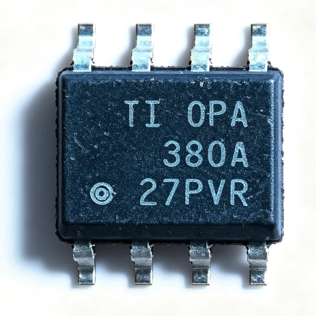
OPA380AID - 90MHz Precision Transimpedance Amplifier | TI
The Texas Instruments OPA380AID is a precision, high-speed transimpedance amplifier in an 8-pin SOIC (D) package, combining a 90MHz gain bandwidth product with extremely high DC precision for fast photodiode applications. It converts photodiode currents up to 1mA into voltage signals with transimpedance bandwidth exceeding 1MHz. A transimpedance amplifier (TIA) is a specialized current-to-voltage converter built on an operational amplifier with a feedback resistor, forming the analog front end of optical receivers, barcode scanners, and photodiode-based instruments. Within the signal-chain hierarchy, the TIA sits between the photodetector and the ADC or comparator, and its noise, bandwidth, and offset set the dynamic range of the whole optical link. Key features include 50pA maximum input bias current, 25uV maximum offset voltage, and 0.1uV/C maximum drift, giving 4 to 5 decades of dynamic range. The very low 1/f noise and excellent long-term Vos stability result from an internal auto-zero amplifier cascaded with a high-speed amplifier, rather than a traditional composite approach, improving overload recovery and settling time. The auto-zero plus high-speed composite architecture eliminates the usual precision-versus-speed trade-off: DC accuracy typical of chopper amplifiers is retained while delivering >1MHz transimpedance bandwidth. Quiescent current is 6.5mA per amplifier. Typical applications include high-speed photodiode receivers for optical communications, laser rangefinders and LiDAR receivers, barcode and medical CT scanner photodiode front ends, and precision optical power meters. For stable operation, keep the photodiode capacitance and feedback resistor within the datasheet stability region; a small feedback capacitor is usually required, and the output may need a pull-down resistor to include 0V in the output swing.

OPA380AID - 90MHz Precision Transimpedance Amplifier | TI
The Texas Instruments OPA380AID is a precision, high-speed transimpedance amplifier delivered in an 8-pin SOIC package. It combines a 90MHz gain bandwidth (GBW) with extremely high DC precision, providing transimpedance bandwidth above 1MHz for photodiode currents up to 1mA. A transimpedance amplifier (TIA) is a specialized operational amplifier circuit that converts a sensor current, most commonly from a photodiode, into a proportional output voltage. Within the signal-chain hierarchy, the TIA sits between the optical or current-output sensor and the ADC or comparator, and its bandwidth, input bias current, and offset voltage set the system's dynamic range. The OPA380 belongs to the wider family of precision amplifiers and analog front-end ICs in power management of optical receivers. Key features include a maximum input bias current of 50pA, a maximum offset voltage of 25uV with only 0.1uV/degC drift, and 4 to 5 decades of dynamic range. These specs allow direct interface with high-impedance photodiodes without external cancellation circuitry. Architecturally, the OPA380 results from an internal auto-zero amplifier combined with a high-speed amplifier. This composite topology delivers very low 1/f noise and excellent long-term VOS stability while TI's design improves overload recovery and settling time over a traditional discrete composite approach. Typical applications include high-speed photodiode receivers for optical data links, photodiode-based instrumentation such as spectrophotometers and lab photoreceivers, and barcode or LiDAR-style pulse detection where >1MHz transimpedance bandwidth matters. Design tip: the feedback resistor and photodiode capacitance set stability - use the datasheet's feedback capacitor guidance, and note the output swings to within millivolts of ground only on a single supply with load returned to a negative rail or virtual ground.

OPA396 - 1MHz 24uA Precision RRIO Op Amp | Texas Instruments
The Texas Instruments OPA396 is a single, micropower precision operational amplifier featuring rail-to-rail input and output (RRIO) operation. It combines a 1 MHz gain-bandwidth product with an ultra-low quiescent current of 23.5 uA (24 uA typ), packaged in the tiny SC-70-5 (DCK) surface-mount package for space-constrained portable designs. An operational amplifier (op amp) is a high-gain voltage amplifier with differential inputs and a single-ended output, and is a fundamental building block of analog signal conditioning used for amplification, filtering, and buffering. The OPA396 belongs to the precision op amp category, which prioritizes low offset voltage, low drift, and low input bias current. Within the amplifier hierarchy it is a micropower precision op amp, positioned between general-purpose op amps and ultra-low-power nanopower devices, and its RRIO capability maximizes dynamic range in low-voltage systems. Key differentiating specifications include an ultra-low input bias current of 10 fA (CMOS input stage), a maximum offset voltage of 100 uV, and a low offset drift of 1.2 uV/C over temperature. These parameters deliver high DC accuracy in sensor interfaces and transimpedance applications. The device operates from a 1.7 V to 5.5 V single supply and is specified from -40C to +125C, supporting both single-cell battery systems and industrial environments. Technically, the OPA396 uses a CMOS input stage responsible for its femtoampere-level bias current, and a class-AB rail-to-rail output stage providing solid drive at low supply current. Its high speed-to-power ratio (1 MHz bandwidth at 23.5 uA) is exceptional for battery-powered equipment, and unity-gain stability simplifies design-in. It is a member of the OPAx396 family, which includes single (OPA396), dual (OPA2396), and quad (OPA4396) versions for scalable designs. Typical applications include battery-powered instrumentation, photodiode transimpedance amplification where the 10 fA bias current minimizes dark-current error, portable medical devices, and low-power active filters. The rail-to-rail output swings fully at 1.7 V supplies, allowing direct interfacing with ADCs in IoT sensor nodes and wearable electronics. For design-in, decouple the supply with a 0.1 uF capacitor placed close to the supply pin, and account for the noise-gain versus bandwidth trade-off in high-gain configurations. Prices as of 2026-08-30 reflect distributor single-unit and volume pricing shown below.

OPA404KP - Quad Difet Op Amp 6.4MHz 35V/us | Texas Instruments
The Texas Instruments OPA404KP is a quad high-speed precision Difet operational amplifier delivering 6.4MHz bandwidth, 35V/us slew rate, and a maximum offset voltage of +/-750uV in a 14-pin PDIP package. Its input cascode architecture combines FET-class input bias current of +/-4pA maximum with uncompromised high-speed performance, making it one of the few quad precision amplifiers to merge these traits in a single DIP footprint. An operational amplifier (op amp) is a high-gain differential voltage amplifier used to perform analog signal conditioning tasks such as amplification, buffering, filtering, and integration. The OPA404 belongs to the precision amplifier hierarchy: operational amplifier -> precision JFET/Difet amplifier -> analog front-end IC. Quad devices integrate four matched amplifiers on one die, cutting board area and improving channel matching versus four single amplifiers. Key features include 6.4MHz gain-bandwidth, 35V/us slew rate, +/-4pA maximum input bias current, +/-750uV maximum offset voltage, and 0.01% settling performance. The Difet (dielectrically isolated FET) process yields input bias currents orders of magnitude below bipolar designs while retaining wideband dynamics, so the part serves both precision DC and fast AC signal paths simultaneously. The input cascode design maintains precision input specifications at high speed, unlike JFET parts such as the TL074 family, which trade precision for cost. Total supply voltage spans 10V to 36V, supporting +/-15V analog rails and single-supply operation from higher-voltage buses. The standard quad pinout allows direct upgrades of existing TL074/TL084 sockets to higher performance. Typical applications include data acquisition front ends, active filters, photodiode transimpedance amplifiers, and test instrumentation signal chains where four channels must share consistent precision characteristics. Design consideration: with 35V/us slew rate, layout and supply decoupling matter - place 0.1uF ceramic capacitors close to each supply pin, and watch output current limits when driving capacitive loads. This page synthesizes distributor pricing, drop-in alternatives, pinout data, and practical design notes not found in the manufacturer datasheet, as of 2026-09-13.

OPA404KU - Quad 6.4MHz Precision Difet Op-Amp | Texas Instruments
The Texas Instruments OPA404KU is a quad high-speed precision Difet (dielectrically-isolated FET) operational amplifier delivering 6.4 MHz bandwidth, 35 V/us slew rate, and a maximum input offset voltage of +/-750 uV, housed in a 16-pin SOIC package with the industry-standard quad op-amp pinout. A Difet operational amplifier is a precision op-amp built on dielectrically isolated FET process technology. Within the signal-chain hierarchy, the OPA404 belongs to the class of precision amplifiers: operational amplifier -> precision op-amp -> high-speed precision amplifier -> analog front-end IC. Unlike JFET-input op-amps fabricated on standard junction-isolated processes, Difet technology couples extremely low input bias current with wideband dynamics, a combination historically difficult to achieve in a single monolithic device. Key differentiating specifications include the 6.4 MHz wide bandwidth, 35 V/us high slew rate, +/-750 uV maximum offset voltage, +/-4 pA maximum input bias current, and 0.01% low settling time. This combination makes the device suitable when engineers need FET-input precision without sacrificing the speed of general-purpose high-speed amplifiers. Supply operation spans +/-5V to +/-18V (10 V to 36 V total), covering most analog instrumentation rails. Architecturally, the dielectrically isolated FET inputs contribute picoampere-level bias currents, which preserve accuracy when the amplifier is driven from high-impedance sources such as photodiodes, piezoelectric sensors, and high-value resistor networks. The standard quad pinout allows designers to drop the part into existing quad op-amp layouts originally designed around devices like the TL074 or TLC274, upgrading precision without PCB redesign. Typical applications include data acquisition front ends, precision integrators and active filters, photodiode transimpedance amplifiers, test and measurement instrumentation, and multi-channel audio or industrial signal processing where four matched channels in one package save board area and improve channel-to-channel matching. Design considerations: because input bias current is only a few picoamperes, use guard rings and clean board layout to prevent leakage paths from dominating the input error budget. Verify stability with capacitive loads and set gain appropriately for the 6.4 MHz bandwidth. This page synthesizes distributor pricing, verified alternatives, pinout data, and practical design notes not found in a single manufacturer datasheet, providing a one-stop engineering reference for the OPA404KU.
OPA404KU/1K - Quad 6.4MHz Precision Difet Op Amp | TI
The Texas Instruments OPA404KU/1K is a quad high-speed precision Difet (dielectrically-isolated FET) operational amplifier delivering 6.4 MHz bandwidth, 35 V/us slew rate, and +/-750 uV maximum offset voltage in a 16-pin SOIC (DW) package rated 0C to +70C. A precision operational amplifier is a differential-input, high-gain voltage amplifier built around a FET or bipolar input stage that minimizes DC error terms such as offset voltage and input bias current. Within the signal-chain hierarchy, op amps sit between sensors/ADCs and the wider analog front end, making their DC accuracy and dynamic performance critical to overall system precision. The Difet process uses dielectric isolation of the input FETs, which reduces input bias current far below what junction-isolated JFET processes achieve. Key features include an unusually low maximum input bias current of +/-4 pA, 0.01% settling to fast accuracy levels, unity-gain stability, and a standard quad op amp pinout that allows direct upgrading of existing designs. The combination of low bias current with wide bandwidth and fast slew rate in a single quad package is rare and eliminates matching multiple singles. Technically, the dielectrically isolated FET input stage keeps bias current low over temperature and input range, while the internal compensation guarantees stability down to unity gain without external capacitors. The standard quad pin configuration (outputs on pins 1, 7, 8, 14) preserves compatibility with legacy quad sockets. Typical applications include precision instrumentation, optoelectronics, sonar and ultrasound front ends, professional audio equipment, medical equipment, and detector arrays. Design consideration: as a quad device, ensure each amplifier channel has proper supply decoupling, and account for the 0C to +70C commercial operating range - the industrial-range variant OPA404KU/1KE4-grade equivalents should be evaluated for extended temperature designs. This page synthesizes distributor pricing, verified drop-in alternatives, pinout data, and practical design notes not consolidated in the manufacturer datasheet.
OPA404SG - Quad 6.4MHz Precision Difet Op Amp | Texas Instruments
The Texas Instruments OPA404SG is a quad high-speed precision Difet (dielectrically isolated FET) operational amplifier delivering 6.4 MHz bandwidth, 35 V/us slew rate, and a maximum input offset voltage of +/-750 uV in a 14-pin CDIP (ceramic dual-in-line) package. An operational amplifier is a high-gain differential voltage amplifier that forms the foundational building block of the analog signal chain, sitting within the broader hierarchy of linear amplifiers and amplifier ICs in power management and signal conditioning systems. Quad op amps integrate four independent amplifier channels on a single die, sharing supply pins while keeping inputs and outputs independent, which reduces board area and improves channel-to-channel matching in multi-channel analog designs. Key features of the OPA404 include a wide 6.4 MHz bandwidth, a fast 35 V/us slew rate, low input bias current of +/-4 pA max enabled by the Difet input cascode architecture, 0.01% settling to fast accuracy, and a standard quad op amp pin configuration that allows direct upgrading of existing designs. The Difet (dielectrically isolated FET) process eliminates the junction-isolation leakage and parasitic capacitance of conventional processes, combining precision input specifications with uncompromised high-speed performance. The input cascode design keeps the drain-source voltage of the input FETs constant, stabilizing input bias current over temperature and common-mode range while preserving bandwidth. The SG suffix denotes the military-grade temperature rating in a hermetic ceramic package, supporting extended-temperature operation where plastic packaging is unacceptable, such as defense and aerospace instrumentation. Typical applications include high-speed data acquisition front ends, active filters in test and measurement equipment, precision integrators, photodiode transimpedance amplifiers, and multichannel buffer stages in industrial instrumentation. The quad configuration is particularly efficient in filter topologies such as state-variable designs that require four amplifiers per channel set. Design consideration: although the 4 pA bias current permits very large feedback resistors, resistor values above approximately 10 megaohm should be evaluated against parasitic capacitance effects on stability; use short feedback traces and consider a small feedback capacitor. This page synthesizes distributor availability, drop-in alternative analysis, and practical design guidance beyond what the manufacturer datasheet provides.

OPA4140 - Quad 11MHz Low-Noise JFET Precision Op Amp | Texas Instruments
The Texas Instruments OPA4140 is a quad-channel, 11-MHz, low-noise, high-precision JFET-input operational amplifier with rail-to-rail output swing, available in 14-pin SOIC and 14-pin TSSOP packages. It delivers 5.1 nV/√Hz input voltage noise density, 11 MHz gain-bandwidth product, and 20 V/µs slew rate while operating from a single supply of 4.5 V to 36 V or dual supplies of ±2.25 V to ±18 V. The JFET input stage provides 0.5 pA typical input bias current and ±1.5 µV/°C low offset drift, making it suitable for high-impedance sensor front-ends. An operational amplifier (op amp) is an active analog building block that amplifies the difference between two input voltages and drives the result through an output stage. The op-amp hierarchy sits within analog ICs, then linear ICs, then signal-conditioning and power-management ICs. JFET-input op amps form a sub-family that uses a junction field-effect transistor at the differential input pair, giving extremely low input bias current and high input impedance - critical for photodiode, pH-electrode, and high-impedance transducer front-ends that bipolar input stages cannot load correctly. Key features include 0.5 pA input bias current, 0.5 mV maximum input offset voltage (A-grade), unity-gain stability, output swing to within 50 mV of either rail at 10 kΩ load, and short-circuit protection (rated ±18 mA). The device operates across -40 °C to +125 °C and is unity-gain stable for purely resistive or moderate-capacitive loads, eliminating the need for external compensation. Architecturally, the OPA4140 combines a JFET input differential pair with a bipolar second stage and a rail-to-rail class AB output stage. This hybrid topology achieves the low bias current of JFET, the low noise and precision of bipolar, and the wide output swing that lets a single 5 V rail power ADC drivers and reference buffers without external level shifters. Typical applications include precision analog front-ends (weigh scales, strain gauges, temperature loggers), battery-powered instrumentation, photodiode transimpedance amplifiers, and active filters or integrators in test equipment. Designers choose the OPA4140 over bipolar alternatives when the source impedance exceeds 10 kΩ. When routing the PCB, place 0.1 µF ceramic bypass capacitors within 5 mm of each supply pin and keep input traces short to preserve the 5.1 nV/√Hz noise floor. Use a ground plane under the package to shield inputs from digital noise, and respect the input common-mode range that extends to the negative rail. This page synthesizes distributor pricing, drop-in same-family alternatives, and practical design notes that complement the manufacturer datasheet.

OPA4140AID - Quad 11MHz 36V JFET Op Amp | Texas Instruments
The Texas Instruments OPA4140AID is a quad-channel, 11-MHz, low-noise, 36-V JFET precision operational amplifier with rail-to-rail output, housed in a 14-pin SOIC (D) package. It features 5.1 nV/√Hz input voltage noise density, 1 pA typical input bias current (JFET input stage), 20 V/µs slew rate, and operates from ±2.25 V to ±18 V dual supplies or 4.5 V to 36 V single supply. A JFET input operational amplifier is a precision analog building block that uses a junction field-effect transistor at its input stage instead of a bipolar transistor. This architecture delivers very low input bias current (picoampere range) and high input impedance, which is critical when amplifying signals from high-impedance sensors, photodiodes, or transducer bridges without loading the source. The OPAx140 family (single, dual, quad) extends this JFET topology into a low-power, low-noise, rail-to-rail-output design suited for modern single-supply precision instrumentation. Key differentiating features include 5.1 nV/√Hz voltage noise density, 11 MHz gain-bandwidth product, 20 V/µs slew rate, ±18 V (36 V) supply operation, true rail-to-rail output swing, low 1.8 mA per-channel quiescent current, and excellent DC precision with 5 µV typical offset voltage. The JFET input stage eliminates the high input bias currents seen in bipolar amplifiers, making the OPA4140 ideal for high-impedance sensor signal chains. Technically, the OPA4140 uses TI's proprietary JFET-input dielectrically-isolated process combined with a precision laser-trimmed input stage. The architecture provides unity-gain stability, integrated EMI/RFI rejection filtering, and shutdown-free always-on operation. Each channel draws a low 1.8 mA quiescent current, enabling multi-channel precision designs without thermal concerns in compact 14-SOIC layouts. Typical applications include precision instrumentation amplifiers, multi-channel data acquisition systems, medical and analytical instrumentation, high-impedance transducer front-ends, professional audio line drivers, active filters, and precision ATE reference buffers. The four channels in one package support dense PCB layouts for multi-sensor or multi-axis measurement systems. When designing with this device, route input traces as guarded differential pairs and use a solid ground plane to preserve the JFET input's high-impedance advantage. Add 100 nF ceramic bypass capacitors close to each supply pin to maintain PSRR and prevent oscillation under capacitive loads above 1 nF. This page synthesizes distributor pricing, drop-in quad-channel alternatives, and practical design notes for the OPA4140AID that are not collated in the manufacturer datasheet alone.
OPA4140AIPW - Quad 11MHz JFET Precision Op Amp | Texas Instruments
The Texas Instruments OPA4140AIPW is a quad-channel, 11-MHz, low-noise, 36-V JFET-input precision operational amplifier with rail-to-rail output, packaged in a 14-pin TSSOP (PW) bulk format. The OPAx140 family features 5.1 nV/√Hz voltage noise density, 1 µV/°C maximum offset drift, 120 µV maximum input offset voltage, and 10 pA maximum input bias current over the full operating temperature range. With a 20 V/µs slew rate and 11 MHz gain-bandwidth product, the device delivers high-speed precision for demanding signal-chain applications. A JFET-input operational amplifier is a class of analog amplifier that uses junction field-effect transistors at the input stage to deliver very high input impedance (giga-ohm range) and exceptionally low input bias current. JFET op amps sit within the broader hierarchy of operational amplifiers -> linear amplifiers -> analog ICs -> semiconductor devices. Compared to bipolar-input op amps, JFET inputs avoid the picoamp-to-nanoamp bias currents of BJT inputs and excel in high-impedance sensor interfaces, transimpedance amplifiers, and precision integrators. Key features include rail-to-rail swing that allows designers to maximize dynamic range on low-voltage single supplies (down to 4.5 V), an input common-mode range that includes the negative supply (V-), and a quiescent current of approximately 1.8 mA per channel. The combination of 5.1 nV/√Hz noise and 1 µV/°C drift positions this part as a premium choice for instrumentation where temperature stability and source-impedance robustness matter. Typical applications include precision analog front-ends for industrial sensors, audio preamplifiers and DAC output buffers, photodiode transimpedance stages, medical instrumentation signal conditioning, and active filters in test-and-measurement equipment. The 36-V absolute-maximum supply also permits ±18 V dual-rail designs in professional audio and industrial process control. When designing with the OPA4140AIPW, choose feedback resistors between 2 kΩ and 100 kΩ to minimize Johnson noise contribution and bias-current offset error. Use 0.1 µF ceramic bypass capacitors within 5 mm of each supply pin to suppress oscillation in high-gain configurations. This page synthesizes verified distributor pricing, drop-in same-package and cross-brand alternatives, and practical design guidance not available from any single distributor listing or datasheet abstract.
OPA4192IPW - 36V Quad Precision RRIO Op Amp | Texas Instruments
The Texas Instruments OPA4192IPW is a 36V, low-noise, low-quiescent-current, rail-to-rail input/output (RRIO) precision operational amplifier with e-trim technology, supplied in a 14-pin TSSOP (PW) package. It belongs to the OPAx192 family (OPA192 single, OPA2192 dual, OPA4192 quad) and delivers 10 MHz unity-gain bandwidth, 20 V/µs slew rate, and ±5 µV typical input offset voltage in a quad-channel configuration. The device operates from 8V (4.5V single-supply equivalent) to 36V (single supply) or ±4V to ±18V (dual supplies). An operational amplifier (op amp) is a high-gain DC-coupled electronic voltage amplifier with differential inputs and a single-ended output that uses external feedback components to set transfer characteristics. Precision op amps form a sub-category optimized for low offset, low drift, low bias current, and low noise, and they sit within the broader hierarchy: operational amplifier -> analog amplifier -> linear IC -> power management & signal chain. The OPAx192 e-trim family improves offset and drift during final test, eliminating the need for the user to null the offset externally. Key differentiating specifications include 5.5 nV/√Hz input voltage noise density at 1 kHz, 1.8 mV maximum input offset voltage over temperature, 5 pA typical input bias current, 1 mA quiescent current per channel, and a robust 36V absolute-maximum supply rating. The RRIO topology swings within a few millivolts of both rails on input and output, simplifying single-supply designs and maximizing dynamic range when powering low-voltage ADCs from higher analog rails. The OPA4192 uses TI's e-trim trimming process combined with a CMOS input stage, providing low input bias current (5 pA typical) and low noise without the drawbacks of traditional JFET or bipolar input stages. Its MUX-friendly input architecture prevents input over-voltage back-flow to the supply when the input exceeds the rails, allowing the device to sit on the same signal bus as switched-capacitor multiplexers without interaction. Typical applications include precision analog input modules for industrial PLCs, multi-channel data acquisition front ends, instrumentation signal conditioning, active filters and buffers for test & measurement equipment, and transducer amplifiers for pressure, strain-gauge, and thermocouple sensors. The quad channel count is well suited for bridge-type sensors that need excitation buffering plus three instrument amplifiers per channel, or for four-channel analog input modules on factory-automation backplanes. Design considerations include adequate PCB thermal relief for 36V operation, input protection when the source impedance is high, and supply decoupling within 5 mm of each supply pin. The MUX-friendly input eliminates the need for additional series input resistors in many multiplexed applications, simplifying the BOM and reducing board area. This page synthesizes distributor pricing, drop-in alternatives, and practical design notes not found on a typical DigiKey or Mouser product page, giving engineers a one-stop technical summary for the OPA4192IPW.