Semicondutores Discretos
Subcategorias
Produtos (1697)
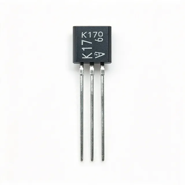
2SK170-GR - N-Channel JFET Low Noise Audio | Toshiba
The Toshiba 2SK170-GR is an N-channel silicon junction field-effect transistor (JFET) purpose-built for low-noise audio amplifier applications, supplied in a 3-pin TO-92 through-hole package. The GR grade designation identifies an Idss (zero-gate-voltage drain current) bin of 2.6 mA to 6.5 mA, the lowest-current grade in the 2SK170 family. A JFET (junction field-effect transistor) is a voltage-controlled semiconductor in which a reverse-biased gate junction controls conduction between source and drain. Unlike MOSFETs, JFETs have no insulating gate oxide, giving them very low 1/f noise and high input impedance - properties that place them at the input stage of the amplifier-device hierarchy, ahead of bipolar transistors for high-impedance, low-noise signal acquisition. The defining feature of the 2SK170-GR is its exceptionally low input-referred noise, which made it a legendary input device for audio preamplifiers, moving-magnet and moving-coil phono stages, and microphone preamps. Its high gate input impedance (in the gigaohm range typical for JFETs) allows direct connection to high-impedance sources, and its low input capacitance preserves high-frequency response in MM cartridge inputs. The GR grade is specifically chosen when the design bias point targets the 2.6-6.5 mA Idss range; designers typically select and match devices within a grade to minimize offset and distortion in differential input pairs. Because it is depletion-mode, the device conducts at Vgs = 0 and is biased with a negative gate-source voltage, simplifying self-bias circuits with a source resistor. Typical applications include discrete audio preamplifier input stages, phono equalizer front ends, condenser microphone buffers, and low-noise measurement front ends. Toshiba has discontinued the 2SK170 family, so the part is commonly sourced as leftover stock or replaced by the Linear Systems LSK170 series. Design tip: because Idss varies widely unit-to-unit, always measure and match Idss across input pairs and set bias at roughly half of Idss for best linearity and noise trade-off. This page synthesizes distributor pricing, verified drop-in alternatives, and practical matching guidance not found in the manufacturer datasheet.

2STF2220 - 1.5A PNP Power Transistor, 20V, SOT-89 | STMicroelectronics
The STMicroelectronics 2STF2220 is a PNP bipolar junction transistor (BJT) manufactured using the proprietary PB-HDC (Power Bipolar High Density Current) technology, delivering exceptional DC current gain combined with very low saturation voltage. Housed in a SOT-89-3 surface-mount package, the 2STF2220 supports a continuous collector current of up to 1.5 A and a collector-emitter breakdown voltage of 20 V, with a maximum power dissipation of 1.4 W. These characteristics make it a versatile high-gain, low-voltage PNP switch for compact, thermally efficient designs. A PNP bipolar transistor is a type of BJT where the base-emitter junction is forward-biased when the base is pulled below the emitter voltage, allowing current to flow from emitter to collector. PNP transistors complement their NPN counterparts and are commonly used in high-side switching, current mirroring, push-pull output stages, and analog signal inversion. The SOT-89-3 package family sits in the discrete semiconductors -> transistors category hierarchy, providing a compact SMD footprint with a thermal pad that improves heat dissipation relative to smaller SOT-23 housings. The 2STF2220 exhibits a DC current gain (hFE) ranging from 200 to 600, allowing reliable switching with very low base drive currents. Its collector-emitter saturation voltage is specified at low millivolt levels under moderate loads, reducing conduction losses and improving efficiency in linear regulators and load switches. The transition frequency of at least 100 MHz supports use in moderate-bandwidth amplifier and switching applications. The combination of high gain and low VCE(sat) simplifies driver design, reducing the need for complex base-drive circuitry. The PB-HDC process technology optimizes the trade-off between current-handling capability and on-state losses, enabling the 2STF2220 to replace larger PNP devices in space-constrained designs. The SOT-89-3 footprint includes a metal tab connected to the collector, which serves as a thermal pad and must be soldered to a copper pour for rated performance. This design philosophy makes the 2STF2220 suitable for portable power management, battery protection circuits, and load switching subsystems. Typical applications include power management in portable and battery-powered devices, low-side/high-side load switching, DC-DC converter peripheral circuits, MOSFET gate drivers, signal amplification in audio front-ends, LED driving stages, and complementary push-pull output stages paired with an NPN device such as the 2STF1360. When designing with this transistor, ensure the collector pad of the SOT-89-3 package is soldered to an adequate copper area to achieve rated thermal performance. Provide a base resistor to limit inrush during turn-on, and respect the maximum emitter-base voltage of 5 V to prevent reverse breakdown of the base-emitter junction. This page synthesizes distributor pricing, drop-in alternative candidates, and practical PCB thermal guidance not found in the standalone manufacturer datasheet, helping engineers quickly evaluate the 2STF2220 for both new designs and replacement scenarios.

2STR2215 - PNP High Current Density Power Transistor | ST
The STMicroelectronics 2STR2215 (sold under part reference 215) is a low-voltage fast-switching PNP power transistor manufactured using ST's proprietary PB-HCD (Power Bipolar High Current Density) technology. According to the STMicroelectronics datasheet, this technology delivers exceptional high-gain performance coupled with very low saturation voltage, making the device well suited for switching and linear power stages where conduction losses must be minimized. A PNP power transistor is a bipolar junction transistor (BJT) in which the majority current is carried by holes; it is turned on by pulling the base below the emitter potential. In the power-management hierarchy, power BJTs sit alongside MOSFETs and IGBTs as discrete power semiconductors, and PNP types are frequently paired with complementary NPN devices in push-pull outputs, linear regulators, motor drivers, and general-purpose switching circuits. The defining characteristics of the 2STR2215 are its high current gain, which reduces base-drive requirements and simplifies driver circuitry, and its very low collector-emitter saturation voltage, which reduces on-state power dissipation and improves overall efficiency in switch-mode and low-voltage applications. The fast-switching classification also makes it suitable for applications requiring quick turn-on and turn-off transitions. The complementary NPN device is the 2STR1215, allowing designers to build matched push-pull or half-bridge stages with symmetric gain and saturation characteristics. This complementary pairing simplifies thermal and electrical matching in class-AB output stages and driver applications. Typical applications include low-voltage switching regulators, power-supply output stages, motor and actuator drivers, and general-purpose amplification where a robust PNP device with low VCE(sat) is required. When designing with the 2STR2215, verify the safe operating area against the actual load current and supply voltage, and ensure adequate base-drive current to keep the device in saturation under worst-case load conditions, since insufficient drive raises VCE(sat) and junction temperature. This page synthesizes verified datasheet information, sourcing guidance, and drop-in alternative analysis not consolidated in the manufacturer datasheet.

551 - Surface Mount Schottky Diode 20V 500mA SOD-323
The Pan Jit International 551 (RB551V-30-AU_R1_000A1) is a surface-mount Schottky barrier diode rated at 20 V reverse voltage and 500 mA average rectified forward current, packaged in a SOD-323 small-outline surface-mount case. Per the manufacturer datasheet, it is designed for low-power rectification, freewheeling, and reverse-polarity protection in compact consumer, portable, and industrial designs. The 551 marking identifies the part as a 30 V-class Schottky diode with low forward voltage drop, making it suitable for high-efficiency DC-DC conversion stages where switching and conduction losses must be minimized. A Schottky barrier diode is a semiconductor device that uses a metal-semiconductor junction instead of a PN junction to achieve switching behavior. This construction yields a lower forward voltage (typically 0.3-0.5 V compared to 0.7 V for silicon PN diodes) and essentially zero reverse recovery time, which makes Schottky diodes ideal for high-frequency switch-mode power supplies, OR-ing circuits, and low-voltage rectification. As a member of the Schottky diode family, the 551 sits within the broader taxonomy of diodes -> discrete semiconductors -> semiconductor devices. Key features of the 551 include a 20 V reverse voltage rating (with a typical working peak reverse voltage of 30 V per the manufacturer's 551-marking datasheet), 500 mA continuous forward current, low forward voltage drop (VF approximately 0.35 V at low current), and ultra-fast switching with negligible reverse recovery charge. The SOD-323 package provides a low-profile surface-mount footprint suitable for handheld and portable equipment, while operating across a typical -55C to +125C junction temperature range. Technically, the device uses a planar Schottky barrier construction that minimizes junction capacitance and provides stable forward characteristics. The low capacitance makes the 551 well-suited for use in switching regulators up to several hundred kHz, and the part is commonly placed across an inductive load as a freewheeling diode to protect switching transistors from back-EMF. Typical applications include reverse-polarity protection in USB ports and lithium-ion battery packs, freewheeling diodes in buck/boost converters, signal clamping in ESD-sensitive interfaces, low-voltage rectification in handheld electronics, and OR-ing diodes in redundant power architectures. Designers select the 551 when a compact, low-VF, fast-switching rectifier is needed where a standard recovery rectifier would waste too much power. When designing with the 551, note that the SOD-323 package has limited thermal mass; ensure that the average forward current does not exceed 500 mA and that the junction temperature stays within rated limits at worst-case ambient. Place the part close to the source of transient energy for effective freewheeling, and respect the 20 V reverse voltage ceiling to avoid catastrophic reverse breakdown. This page synthesizes distributor pricing, drop-in alternatives, and practical design notes not found on the manufacturer's brief datasheet, enabling faster BOM decisions for engineers who need a small-footprint Schottky rectifier.
5SGA06C2501 - 2500V Asymmetric GTO Thyristor | ABB
The ABB 5SGA06C2501 is an asymmetric gate turn-off (GTO) thyristor rated at 2500 V off-state voltage and 600 A average on-state current, packaged in an industry-standard press-pack (hockey puck) disc housing. It is a member of ABB's 5SGA GTO family designed for high-voltage, high-current traction, industrial drives, and HVDC converter applications where forced commutation via the gate is required. A GTO (Gate Turn-Off) thyristor is a four-layer PNPN semiconductor device capable of being switched both ON and OFF by a gate control signal, unlike a conventional SCR which only latches on. The 'asymmetric' designation means the reverse blocking capability is intentionally limited (typically a few hundred volts) because GTOs are normally used with an anti-parallel diode, allowing the device to be optimized for low on-state voltage drop and fast turn-off in forward-conduction applications. GTOs sit within the thyristor hierarchy (thyristor -> power semiconductor -> discrete semiconductor) and remain relevant where very high surge currents and short-circuit withstand are required. Key specifications include a repetitive peak off-state voltage (VDRM) of 2500 V, an RMS on-state current (IT(RMS)) up to 940 A, a typical on-state voltage of 3.2 V at the rated current, and a turn-off time in the order of 20-25 µs. The disc package supports double-sided cooling via matched heatsink clamps, enabling symmetrical thermal performance and straightforward series stacking for higher voltage converters. Integrated gate and cathode auxiliary connections simplify the snubber, gate-drive, and protection network layout. Typical applications include three-level NPC traction inverters for rail propulsion, large AC drives for rolling mills and mine hoists, static VAR compensators (SVC) and HVDC valve groups, soft-starters for very large motors, and pulse-power supplies. Designers select the 5SGA06C2501 when an established, field-proven GTO platform is required, when the system voltage exceeds 2000 V series stacking, or when replacement of an aging press-pack device must fit the existing heatsink and clamping hardware. Design consideration: the GTO requires a sizable RC snubber across the device and a well-defined dv/dt and di/dt limit at turn-off; a clamp circuit with MOV or RCD plus a low-impedance gate-cathode return is essential for reliable commutation. Mounting torque, heatsink flatness, and double-sided clamping pressure must follow the manufacturer guideline to achieve the published thermal resistance and to avoid contact wear. This page synthesizes distributor availability, drop-in alternatives, and practical design notes for the 5SGA06C2501 that are not consolidated in the manufacturer datasheet alone.
5SJA3000L520300 - 5200V 3000A Press-Pack IGBT StakPak Module | ABB
The ABB 5SJA3000L520300 is a 5200 V, 3000 A press-pack IGBT (BIGT) StakPak module engineered for high-power traction, HVDC, and industrial drives. The device integrates a low-loss rugged BIGT chip with a 1:1 IGBT-to-diode ratio, a typical VCE(sat) of 3.1 V at 125 C, and a typical forward diode drop VF of 2.52 V at 125 C. It is optimized for low switching-frequency operation with smooth switching behavior for excellent EMC, packaged in a high-tolerance explosion-resistant press-pack housing. A press-pack IGBT is a hermetically sealed, pressure-contacted power module designed for sub-microsecond switching at megawatt power levels. Unlike soldered wire-bond modules, press-pack cells transfer heat and current through a clamped stack, eliminating bond-wire lift and solder-fatigue failure modes. Within the broader taxonomy, the 5SJA3000L520300 is a discrete power semiconductor (IGBT), itself part of the bipolar power-device family that includes GTOs, IGCTs, and BIGTs, and ultimately sits inside the power electronics stack feeding HVDC converters, large motor drives, and traction inverters. Key features of the 5SJA3000L520300 include the low-loss rugged BIGT chip, which combines IGBT and freewheeling diode functions into a single optimized silicon die; high tolerance to uneven mounting pressure across the stacked heatsink interface; an explosion-resistant package that remains in low impedance for up to 1 minute after short-circuit failure, giving the converter a defined short-circuit failure mode instead of an open one. The part targets converters running in the few-hundred-Hz range where conduction loss dominates over switching loss. From a system architecture standpoint, the StakPak platform stacks multiple BIGT wafers in series and parallel inside a single housing to reach 5.2 kV class / 3 kA class operation. ABB's BIGT is a monolithically integrated reverse-conducting IGBT that halves the conduction losses of conventional IGBT+diode pairs, which is critical at low switching frequency where conduction loss dominates. The press-pack package is also short-circuit failure mode (SCFM) rated for safe end-of-life behavior in series-connected HVDC stacks. Typical end-use applications include HVDC valve sections, multi-MW industrial drives (rolling mills, marine propulsion, mining hoists), and railway traction converters. The 5.2 kV class rating allows direct connection to 4.16 kV AC grid rectifiers and 3.3 kV / 6.6 kV motor terminals via series stacking. The smooth-switching BIGT also relaxes snubber and dv/dt-filter requirements at the system level. When designing with this module, mechanical stack pressure is the dominant reliability parameter - the press-pack requires a controlled, uniform clamping force across the contact surface to maintain thermal and electrical performance over decades of thermal cycling. Follow the ABB StakPak assembly guideline for clamp force, surface finish, and heatsink flatness to reach the rated 3000 A collector current. This page synthesizes distributor pricing, BIGT chip-level parameters, and press-pack mechanical design notes that are not consolidated in the manufacturer datasheet alone.
5SNG0450R17030 - 1700V LoPak1 Phase-Leg IGBT Module | ABB
The ABB 5SNG0450R17030 is a 1700 V LoPak1 phase-leg IGBT power module rated at 2 x 450 A continuous collector current, built around ABB's ultra low-loss, rugged SPT++ chip-set. Housed in an industry-standard LoPak1 package with press-fit auxiliary control pins and a copper base-plate, the module integrates a phase-leg (half-bridge) configuration together with a built-in NTC thermistor for temperature sensing and anti-parallel freewheeling diodes on each switch position. The 1700 V VCES rating makes the module a direct fit for 690 V AC line-voltage industrial drives and renewable-energy converters. An Insulated Gate Bipolar Transistor (IGBT) is a voltage-controlled semiconductor switch that combines the high-current, low-saturation characteristics of a bipolar transistor with the simple gate-drive requirements of a MOSFET. In the broader semiconductor taxonomy, an IGBT is a type of power transistor that sits between the MOSFET and the thyristor families, optimized for medium-frequency (1-30 kHz), medium-to-high power (1 kW to >1 MW) switching. Phase-leg IGBT modules combine two IGBT switches and their anti-parallel diodes into a single package, forming the basic building block of voltage-sourced inverters used in motor drives, solar inverters, UPS systems, and induction-heating converters. Key features of the 5SNG0450R17030 include VCEsat of 2.6 V (per the Vyrian listing), nominal turn-on time (ton) of 365 ns, press-fit control pins for reliable auxiliary contacts that eliminate hand-soldering on high-current modules, an integrated NTC thermistor for closed-loop thermal monitoring, and a copper base-plate providing low thermal resistance. The LoPak1 outline is widely adopted across industrial converters, allowing direct mechanical replacement in existing inverter designs. SPT++ (Soft-Punch-Through Plus Plus) is ABB's third-generation soft-punch-through IGBT cell that combines a thin wafer, field-stop layer, and an enhanced backside buffer to deliver lower VCEsat at higher current densities than earlier NPT (Non-Punch-Through) generations. The trade-off is a slightly softer switching tail current, which is acceptable for motor-drive and solar-inverter switching frequencies around 2-8 kHz. For higher switching frequencies (15-30 kHz) in resonant or totem-pole PFC applications, ABB typically recommends the HiPak or LinPak platforms with SiC or Si fast IGBT variants instead. Typical applications for the 5SNG0450R17030 include 690 V AC industrial motor drives, three-phase solar inverters, three-phase UPS systems, induction-heating inverters, and active front-end rectifiers. Its 1700 V VCES provides the necessary voltage margin for 690 V AC bus voltages, including the switching overshoot and DC-link ripple typically seen in regenerative drives. When designing with this module, calculate worst-case conduction and switching losses at the actual switching frequency, then verify that the heatsink keeps the base-plate below 125 C at full load. Use the integrated NTC thermistor for overtemperature protection and the press-fit pins for the gate-driver interface - never solder control pins on a press-fit module as the thermal mismatch will crack the joint during thermal cycling. This page synthesizes ABB datasheet data, distributor listings, and application notes with practical PCB and thermal design guidance not aggregated on a single manufacturer page, plus a curated alternative list to help engineers handle sourcing or second-source decisions for LoPak1 form-factor designs.
6MBI300U4-120 - 1200V 300A 6-in-1 IGBT Module | Fuji Electric
The Fuji Electric 6MBI300U4-120 is a 1200 V, 300 A U-series IGBT power module in a six-in-one (6-unit) package, integrating a three-phase inverter bridge with built-in thermistor temperature sensing and 29 terminals for high-power conversion. An IGBT (Insulated Gate Bipolar Transistor) module combines multiple IGBT dies and freewheeling diodes on an isolated substrate within a single molded housing, sitting at the top of the power semiconductor hierarchy: discrete IGBT -> IGBT chip set -> power module -> power conversion system. Modules simplify thermal design, reduce stray inductance, and provide certified isolation between the silicon and the heatsink surface. Key features of the 6MBI300U4-120 include a collector-emitter voltage rating of 1.2 kV, a maximum collector current of 450 A (absolute maximum), high-speed voltage-drive switching, and a low-inductance module structure that minimizes voltage overshoot during turn-off. The integrated thermistor enables real-time heatsink temperature monitoring for protection and derating logic, and the maximum operating junction temperature is 150 C. The U-series construction uses Fuji Electric's optimized IGBT and FWD chips for a favorable trade-off between conduction losses (low VCE(sat)) and switching losses, making the module well suited to hard-switched PWM inverters driven by standard gate drivers. The low-inductance layout supports fast di/dt events without excessive transient voltages when paired with proper DC-link snubbering. Typical applications include three-phase AC motor drives (VFDs), servo amplifiers, industrial UPS systems, welding power supplies, and renewable-energy power conversion stages operating from 1200 V-class DC buses. The 300 A continuous rating with 450 A peak capability covers mid- to high-power inverter stages in the tens of kilowatts range. Design consideration: always operate within absolute maximum ratings for voltage, current, and temperature, and connect an adequate fuse or circuit protector as required by the datasheet safety guidance; verify square operating area limits against your worst-case load and fault conditions. This page synthesizes distributor availability, drop-in variant alternatives, comparison data, and practical design notes not consolidated in the manufacturer datasheet.
7MBP150RA-120 - IGBT-IPM 1200V 150A 7-in-1 | Fuji Electric
The Fuji Electric 7MBP150RA-120 is a 1200 V, 150 A Intelligent Power Module (IGBT-IPM) of the R series integrating seven power devices in one package (a six-unit three-phase inverter bridge plus a seventh braking chopper unit) with built-in gate drive and protection circuitry. An Intelligent Power Module (IPM) is a power semiconductor module that combines an insulated-gate bipolar transistor (IGBT) power stage with integrated control, gate-drive, and protection circuits in a single insulated package. Within the power-electronics hierarchy, an IPM sits above discrete IGBTs and below full drive systems: a power module -> power management IC -> power conversion system. The IPM format eliminates external gate-driver design, shortens development time, and reduces part count. Key features include junction-temperature protection achieved by directly sensing the IGBT chip temperature, low power loss with soft switching for reduced EMI, and higher reliability through a large decrease in the number of parts in the built-in control circuit. The 1200 V collector-emitter rating suits 380-480 V AC industrial buses, while the 150 A collector current (at Tc = 25 C) and 1040 W maximum power dissipation cover high-power drive stages. Technically, the module integrates N-channel IGBTs with embedded overcurrent (OC/SC), undervoltage (UV), and overtemperature (OT) protection, and it issues a fault output (ALM). Integrated drive removes the need for discrete gate resistors and optocoupler isolation stages on the low-side, improving consistency across production units. Typical applications include industrial AC motor drives (VFD/inverter stages), servo amplifiers, and regenerative braking chopper circuits in general-purpose inverters where the seventh braking unit is used. A key design consideration: keep the control-supply Vcc at 15 V as used in the datasheet electrical-characteristics conditions, and provide adequate heatsinking because power dissipation reaches 1040 W under absolute-maximum conditions. This page adds distributor sourcing context, replacement guidance, and practical design notes not found in the manufacturer datasheet.
A2T26H160-24SR3 - 28W Airfast LDMOS 2496-2690 MHz | NXP
The NXP A2T26H160-24SR3 is a 28 W asymmetrical Doherty RF power LDMOS transistor engineered for cellular base station power amplifiers operating across the 2496 to 2690 MHz band. It is an N-channel enhancement-mode lateral MOSFET housed in the NI-780S-4L2L ceramic package, rated for 28 V operation and delivering typical 15.5 dB power gain at 2.58 GHz with 28 W average output power. The device is built on NXP's Airfast generation of LDMOS technology, optimized for high-efficiency Doherty topologies where peak and carrier amplifiers must be tightly matched in gain, phase, and thermal behavior. An RF power LDMOS transistor (Laterally Diffused Metal-Oxide Semiconductor) is a specialized power MOSFET designed to deliver high RF output power at microwave frequencies while maintaining acceptable gain and efficiency. Within the broader hierarchy, an LDMOS power transistor belongs to the discrete RF power transistor family, itself a subset of power semiconductors used in wireless infrastructure. Doherty amplifier architectures combine a main (carrier) amplifier with an auxiliary (peak) amplifier to maintain high efficiency across a wide output-power back-off range, making LDMOS the dominant technology for 4G LTE and 5G NR base station RF front-ends below 4 GHz. Key features of the A2T26H160-24SR3 include integrated input and output matching networks simplified by the ceramic NI-780S package, broadband capability across the full 2496-2690 MHz band, and high breakdown voltage tolerance that allows reliable operation at the 28 V supply rail typical of macro-cell base stations. The transistor is designed for asymmetrical Doherty operation, meaning the peak amplifier is sized larger than the carrier to handle the peak-to-average ratio (PAR) of modern LTE signals, with appropriate gain matching between the two paths. Its internal matching reduces the bill of materials required at the PCB level. Architecturally, the device uses NXP's seventh-generation Airfast LDMOS process, which delivers higher power density, lower parasitic capacitance, and improved thermal performance compared to earlier Airfast generations. The lateral structure provides excellent gain flatness across the band, while the enhancement-mode gate design simplifies bias circuits by eliminating the need for negative gate voltages during operation. Typical applications include 4G LTE and 5G NR macro-cell base stations, small-cell and massive-MIMO antenna arrays, and Doherty final-stage power amplifier modules for the 2.5-2.7 GHz international wireless bands (Bands 38, 41, and n78). The device is also used in repeaters and boost amplifiers where linearity and efficiency across modulation bandwidths are critical. When designing with this LDMOS, ensure adequate copper heat-spreading under the ceramic flange and use a thermal interface material with low thermal resistance. Bias sequencing should follow NXP's reference design: drain voltage applied first, then gate quiescent current set to the recommended IDQ for Doherty operation, and RF input applied only after both rails are stable. This page synthesizes distributor pricing, drop-in pin-compatible alternatives, thermal design notes, and Doherty integration guidance not consolidated in the manufacturer datasheet, giving RF power amplifier design engineers a single reference for component selection, sourcing, and layout planning.

AB - SOT-23 Marking Code | MMBZ5226B Zener Diode | Semtech
The marking code "AB" identifies the MMBZ5226B (Semtech Corporation), a silicon planar Zener diode housed in a 3-pin SOT-23 surface-mount package. According to the manufacturer datasheet (3 pages), the MMBZ5226B series provides a nominal Zener voltage of 3.3 V with a tight tolerance and is intended for voltage regulation, clamping, and reference functions in compact electronic assemblies. A Zener diode is a specialized silicon PN-junction diode engineered to operate in reverse breakdown at a defined voltage. Within the broader semiconductor taxonomy, Zener diodes sit under discrete semiconductors -> diodes -> voltage reference diodes. They are used to clamp voltage excursions, establish stable reference rails, and protect downstream circuitry from ESD or transient over-voltage events. Key features of the MMBZ5226B (AB marking) include a nominal Zener voltage of 3.3 V at the standard test current, low leakage current in the forward-biased region, and a SOT-23 outline that enables high-density PCB placement. The part shares its footprint with thousands of other SOT-23 devices, allowing drop-in substitution across many low-voltage regulator or reference circuits. The architecture is a planar silicon die with controlled doping to set the breakdown voltage, then wire-bonded into the SOT-23 lead frame. The small package provides moderate thermal dissipation suitable for low-current regulator applications but limits continuous power dissipation, which must be respected in the PCB layout. Typical applications include 3.3 V reference generation in portable electronics, voltage clamping on data lines, ESD protection for handheld devices, and bias reference in low-power analog circuits. Designers select this part when board space is constrained and a compact, well-characterized reference voltage is required. When designing with this part, observe the maximum power dissipation rating for the SOT-23 package and ensure PCB copper pad area provides adequate heatsinking. For applications requiring tight tolerance or higher power, verify the test current and dynamic impedance in the manufacturer datasheet. This page synthesizes distributor inventory, drop-in SOT-23 alternatives with the same footprint, and design guidance that complements the manufacturer datasheet rather than simply repeating it.
ADR5044WBRTZ-R7 - 4.096V Shunt Voltage Reference, ±0.1% | ADI
The Analog Devices ADR5044WBRTZ-R7 is a precision micropower shunt voltage reference that provides a fixed 4.096 V output with an initial accuracy of ±0.1% in a 3-pin SOT-23 surface-mount package. Designed for space-critical and battery-powered applications, it operates over a cathode current range from 50 µA minimum to 15 mA maximum and requires no external compensation capacitor for stability, while remaining stable with any capacitive load. A shunt voltage reference is a two-terminal (cathode and anode) device that behaves like a precision Zener diode: it regulates the voltage across its terminals when biased with a current source, and its operating current is set by the external load or bias resistor. Compared with three-terminal series references, shunt references offer lower quiescent draw and simpler noise filtering, but they always draw a small standby current even when the load is off. Within the broader power management IC taxonomy, shunt references sit alongside series (bandgap) references and are used wherever a low-noise, low-drift reference voltage is needed. The key specifications include a maximum temperature coefficient of 75 ppm/°C, an initial accuracy of better than 0.1% (B grade), and an operating temperature range of −40 °C to +125 °C. The "W" grade adds the automotive qualification (AEC-Q100) marker, and "BRTZ" denotes the SOT-23 (RT) package on tape and reel (R7). The advanced buried-Zener bandgap design eliminates the need for an external compensation capacitor and ensures stable operation with capacitive loads, simplifying PCB design in dense analog front ends. Typical applications include automotive sensor signal conditioning, portable and battery-powered instrumentation, precision data acquisition front ends, current-loop (4-20 mA) transmitters, and reference rails for ADCs and DACs in industrial process control. The 4.096 V output is an exact multiple of 2^12, making it a natural fit for 12-bit and 14-bit ADCs that scale a full-scale input of 4.096 V to a 1-LSB step of 1 mV. When designing with this reference, choose the bias resistor so that the cathode current stays between 50 µA and 15 mA under all load conditions. Add a 0.1 µF to 10 µF bypass capacitor directly across the reference to filter wideband noise, even though the device is stable without it. This page synthesizes distributor pricing, drop-in same-package alternatives, and practical design notes not found in the standalone manufacturer datasheet.
ADTC144ECAQ-7 - NPN Pre-Biased BJT, 50V, 100mA, SOT-23 | Diodes Inc
The Diodes Incorporated ADTC144ECAQ-7 is an NPN pre-biased bipolar junction transistor (BJT) housed in a 3-pin SOT-23 surface-mount package, integrating two 47 kΩ bias resistors (R1 = R2) on a single epitaxial planar die. According to the manufacturer datasheet, the device is rated for a collector-emitter voltage of 50 V, continuous collector current of 100 mA, transition frequency of 250 MHz, and total power dissipation of 310 mW, making it suitable for switching and amplification circuits where space and component count are at a premium. A digital transistor (also known as a pre-biased transistor or resistor-equipped transistor, RET) is a BJT with integrated base and base-emitter resistors that replaces a discrete BJT plus two external bias resistors. It belongs to the broader transistor family (BJT > semiconductor > active electronic component). By collapsing three discrete parts into one SOT-23, digital transistors simplify PCB layout, lower BOM count, reduce parasitic inductance, and enable direct logic-level drive from microcontrollers without external bias networks. Key features include built-in 47 kΩ / 47 kΩ bias resistors (R1 = R2), eliminating the need for external base biasing; an epitaxial planar die construction that improves switching performance and minimizes leakage; and AEC-Q101 qualification that makes the part suitable for automotive applications requiring specific change control. The part is also PPAP capable and manufactured in IATF 16949 certified facilities, with totally lead-free, fully RoHS-compliant, halogen-free and antimony-free "green" device construction. Architecturally, the ADTC144ECAQ-7 uses a standard NPN epitaxial planar BJT die with monolithic resistor integration. The 47 kΩ / 47 kΩ ratio means the device is biased to switch on when its input voltage exceeds roughly 0.7 V plus the drop across the bias network, allowing direct interface to 1.8 V, 3.3 V, or 5 V logic. The 250 MHz transition frequency supports medium-speed switching applications including level shifting, interface buffering, and relay/LED driver circuits. Typical applications include digital logic interfacing, MOSFET gate drivers, relay and solenoid drivers, LED indicator drivers, level shifters between logic domains, and inverter stages in automotive body electronics, white goods, and industrial control boards. The automotive-grade qualification broadens use to BCMs, HVAC controls, and instrument cluster signal conditioning. When designing with the ADTC144ECAQ-7, observe the 310 mW power dissipation ceiling, derate above 25 °C ambient, and place the device near the driven load to minimize trace inductance. This page synthesizes distributor pricing, drop-in alternatives, and practical design notes not found in the manufacturer datasheet.

ADUM3223ARWZ - 4A Isolated Half-Bridge Gate Driver | Analog Devices
The ADUM3223ARWZ is a 4 A isolated, half-bridge gate driver from Analog Devices, employing iCoupler technology to provide independent and isolated high-side and low-side outputs. It offers 3000 V rms isolation in a narrow body, 16-lead SOIC package, making it suitable for a wide range of power conversion applications. The device combines high speed CMOS and monolithic transformer technology, delivering robust performance with minimal propagation delay and excellent common-mode transient immunity. An isolated gate driver is a specialized integrated circuit that provides the necessary voltage and current to drive the gate of power transistors (such as MOSFETs and IGBTs) while maintaining galvanic isolation between the control side and the power stage. This isolation is critical in applications where the power stage operates at high voltages or in noisy environments, protecting the low-voltage control circuitry and ensuring safe, reliable operation. Isolated gate drivers are essential components in switch-mode power supplies, motor drives, and inverters, where they enable efficient and safe switching of high-power devices. Key features of the ADUM3223ARWZ include 4 A peak output current, 3000 V rms isolation, and a wide supply voltage range. The device supports both high-side and low-side outputs with independent inputs, allowing flexible control of half-bridge topologies. It also features a high common-mode transient immunity (CMTI) of typically 100 kV/us, ensuring reliable operation in noisy environments. The propagation delay is typically 50 ns, enabling high-frequency switching with minimal timing skew. Technically, the ADUM3223ARWZ integrates Analog Devices' iCoupler technology, which uses chip-scale transformers to transmit signals across the isolation barrier. This approach offers advantages over traditional optocouplers, including higher speed, lower power consumption, and better reliability. The device is designed to drive power MOSFETs and IGBTs directly, with a wide output supply range from 4.5 V to 18 V, accommodating various gate drive requirements. The narrow body SOIC-16 package is compact and suitable for space-constrained designs. Typical applications include isolated switch-mode power supplies, motor drives, solar inverters, and industrial automation. The ADUM3223ARWZ is particularly well-suited for half-bridge and full-bridge topologies where high-side and low-side drivers are required. Its high output current ensures fast switching of large gate capacitances, reducing switching losses and improving efficiency. When designing with this device, it is important to provide adequate decoupling on both the input and output supplies, and to ensure proper layout to minimize parasitic inductance. The device also requires careful consideration of the isolation rating and creepage distances for the target application's safety standards.
ADUM4135BRWZ - 4A Isolated IGBT Gate Driver | Analog Devices
The ADUM4135BRWZ is a single-channel, high-voltage isolated gate driver from Analog Devices, specifically optimized for driving insulated gate bipolar transistors (IGBTs). It utilizes Analog Devices' iCoupler® magnetic isolation technology to provide 5000Vrms isolation between the input and output stages, ensuring safe and reliable operation in high-voltage applications. The device delivers a peak output current of 4A, making it suitable for driving high-power IGBTs and MOSFETs in industrial motor drives, solar inverters, and electric vehicle (EV) charging systems. An isolated gate driver is a specialized integrated circuit that transfers control signals across an isolation barrier while providing the high-current drive needed to switch power transistors. It combines galvanic isolation, typically using magnetic or capacitive coupling, with a high-current output stage. In the hierarchy of power electronics, an isolated gate driver sits between the low-voltage controller (such as a microcontroller or DSP) and the high-voltage power stage, ensuring both signal integrity and safety. The ADuM4135 belongs to the family of isolated gate drivers, which are essential components in power conversion systems. Key features of the ADUM4135BRWZ include a Miller clamp to prevent false turn-on due to the Miller effect, a desaturation (DESAT) protection circuit that detects overcurrent conditions and shuts down the IGBT, and a fault output that signals abnormal operation. The device supports both single-supply and dual-supply configurations, with a wide output supply range from 4.5V to 35V. It also features a common-mode transient immunity (CMTI) of 100 kV/µs, ensuring reliable operation in noisy environments. The ADuM4135 is built using Analog Devices' proprietary iCoupler technology, which uses chip-scale transformers to achieve isolation. This technology provides superior performance compared to optocouplers, including higher data rates, lower power consumption, and better reliability. The device is available in a 16-lead SOIC package (RW-16), which is compact and suitable for space-constrained designs. The operating temperature range is -40°C to +125°C, making it suitable for industrial and automotive applications. Typical applications include IGBT gate drive circuits in motor drives, uninterruptible power supplies (UPS), solar inverters, and welding equipment. The ADUM4135BRWZ is also used in electric vehicle (EV) traction inverters and charging stations, where high isolation and robust protection are critical. Its high output current and fast switching speed enable efficient power conversion, while the integrated protection features enhance system reliability. When designing with the ADUM4135BRWZ, it is important to ensure proper PCB layout to minimize parasitic inductance and maintain signal integrity. The DESAT pin should be connected to the IGBT collector through a high-voltage diode, and the Miller clamp should be connected to the gate to prevent false turn-on. Additionally, the input and output supplies should be adequately decoupled with ceramic capacitors placed close to the device pins.
ADUM4136BRWZ - 4A Isolated IGBT Gate Driver | Analog Devices
The ADUM4136BRWZ is a single-channel, galvanically isolated gate driver from Analog Devices, specifically optimized for driving insulated gate bipolar transistors (IGBTs). It delivers up to 4A peak output current and provides 5000Vrms isolation using Analog Devices' iCoupler technology. The device is available in a 16-SOIC package and supports both unipolar and bipolar secondary supplies, enabling negative gate drive when required. A gate driver is a power amplifier that accepts a low-power input from a controller IC and produces a high-current drive input for the gate of a power transistor. In the context of IGBTs and MOSFETs, the gate driver ensures fast, efficient switching by providing the necessary charge to the gate capacitance. The ADUM4136 integrates isolation, making it a key component in power conversion systems where the control side and power stage must be electrically separated for safety and noise immunity. Key features include a 4A peak output current, 5000Vrms isolation voltage, and a DESAT (desaturation) protection pin that monitors the collector-emitter voltage of the IGBT. When the DESAT pin rises above the 9.2V threshold, a fault registers, and within 200ns, the gate output drives low, protecting the IGBT from short-circuit conditions. The device also features a blanking time of approximately 2μs, which is a typical design choice to prevent false triggering during turn-on transients. The ADUM4136 uses chip-scale transformers for isolation, providing reliable signal transfer across the isolation barrier. It supports both unipolar and bipolar supply configurations, allowing designers to apply negative gate drive voltages to improve noise immunity and reduce switching losses. The propagation delay is typically [DATA_NEEDED: propagation delay], and the device operates over a wide temperature range of -40°C to +125°C. Typical applications include motor drives, solar inverters, uninterruptible power supplies (UPS), and industrial power conversion systems. The high isolation voltage and robust protection features make it suitable for demanding environments where safety and reliability are critical. When designing with the ADUM4136, ensure proper PCB layout to minimize parasitic inductance in the gate drive loop. Place the gate resistor close to the IGBT gate and use a low-impedance return path for the high di/dt currents. Also, consider the DESAT blanking time and adjust the external blanking capacitor to match the IGBT's switching characteristics.
AFT09S282NR3 - 80W 720-960MHz RF LDMOS Transistor | NXP
The NXP Semiconductors AFT09S282NR3 is an 80-watt RF power LDMOS transistor housed in a 3-pin OM-780-2 (NI-780S-style ceramic) surface-mount package with exposed thermal pad, designed for cellular base station applications across the 720-960 MHz frequency range. The device operates from a 28 V nominal supply and is rated for 70 V VDSs, with a typical 20 dB power gain at 960 MHz and 1.4 A DC bias current on the gate. An RF power LDMOS transistor is a laterally diffused metal-oxide-semiconductor power device optimized for high-frequency, high-power amplification. Within the broader taxonomy, it sits at LDMOS -> RF power MOSFET -> power transistor -> discrete semiconductor. LDMOS technology dominates cellular base station power amplification because it offers high gain, high efficiency, and excellent thermal performance compared to silicon bipolar or GaAs alternatives of similar cost. The NXP Airfast AFT09S282NR3 family key features include integrated electrostatic discharge (ESD) protection, an internal input matching network that simplifies board-level design, broadband response across the 720-960 MHz cellular bands, and a high gain-flatness profile. The thermally efficient OM-780-2 ceramic package with a flanged or non-flanged lead offers theta_JC values consistent with extended duty-cycle operation. Architecturally, this is an N-channel enhancement-mode lateral MOSFET. The lateral structure and thick metal field plates reduce on-state losses and improve ruggedness into mismatched loads (VSWR tolerance), enabling reliable operation in Doherty amplifier configurations used at the final stage of macro-cell base stations. Typical applications for the AFT09S282NR3 include single-ended or Doherty power amplifiers in 4G LTE and multi-carrier GSM/EDGE base stations operating in the 900 MHz cellular band (GSM900, cellular 850/900, LTE Band 5/8). Designers also use it for digital video broadcast transmitters and industrial RF heating sources at sub-GHz frequencies. When designing with this part, pay particular attention to thermal management. At full 80 W CW RF output in a Doherty configuration the device dissipates considerable heat; use a copper-molybdenum or copper-tungsten heatsink with proper thermal interface material to keep the junction within the safe operating envelope. This page synthesizes distributor pricing, same-family drop-in alternatives, and Doherty amplifier design notes not found in the manufacturer datasheet - a starting point for engineers evaluating NXP's AFT09S282N family.

AFT18H357-24NR6 - 63W LDMOS RF Power Transistor 1.8GHz | NXP
The NXP AFT18H357-24NR6 is a 63 W asymmetrical Doherty RF power LDMOS transistor designed for cellular base station applications in the 1805 MHz to 1880 MHz band. It is an N-channel enhancement-mode lateral MOSFET housed in an OM-1230-4L2L ceramic air-cavity package, operates from a 28 V drain supply, and delivers 17.5 dB typical power gain at the 1805 MHz test point. The device is engineered for high-efficiency Doherty amplifier topologies where a carrier and peaking amplifier arrangement enables backoff efficiency above what a single-ended PA can achieve. According to the NXP datasheet, the AFT18H357-24NR6 is part of the Airfast 28 V LDMOS RF power family and is targeted at multi-carrier GSM, WCDMA, and LTE base-station PAs that demand high linearity, ruggedness, and thermally stable operation under continuous RF drive. A Doherty amplifier is a two-path RF power amplifier architecture that uses a carrier amplifier biased in Class AB and a peaking amplifier biased in Class C; the two outputs are combined through a quarter-wave impedance inverter so the carrier amplifier sees an apparent load modulation, keeping efficiency high at 6 to 10 dB output backoff compared with a standard Class AB design. This is why cellular base-station PAs prefer asymmetric or symmetric Doherty structures, and why LDMOS (Laterally Diffused Metal-Oxide Semiconductor) transistors dominate macro-cell transmit chains: they offer high gain, high breakdown voltage, and proven reliability at 28 V supplies. The AFT18H357-24NR6 belongs to the broader Airfast 24-series family of N-channel enhancement-mode LDMOS RF power transistors from NXP Semiconductors. Key features include 63 W typical output power (P3dB-class), 17.5 dB power gain at 1.81 GHz, operation over the 1805-1880 MHz frequency band, 28 V typical drain supply, an integrated ESD protection structure, and an air-cavity ceramic package (OM-1230-4L2L) with a copper-flange heatsink interface. The thermal resistance from junction to case is specified to support continuous-wave RF operation in properly cooled base-station environments. The part is rated MSL-3 (Moisture Sensitivity Level 3) and is supplied in tape-and-reel packaging with a peak reflow temperature of 260 C per JEDEC J-STD-020. The asymmetric Doherty architecture of the AFT18H357-24NR6 is built around the 28 V LDMOS process, which NXP optimized for cellular base-station linearity and ruggedness. The device integrates input and output matching structures external to the die, and the flanged ceramic package provides a low-inductance source connection through the package mounting flange. Reliability is qualified to the standards typically applied to NXP Airfast RF power products, including high-temperature operating-life and RF overdrive stress profiles. Typical applications include 4G LTE and 5G NR (sub-6 GHz band 3 / downlink 1805-1880 MHz) macro-cell base-station power amplifiers, multi-carrier GSM and WCDMA transmit chains, asymmetric Doherty final stages in remote radio heads, and high-power amplifier driver or output stages where 28 V LDMOS reliability is required. The 1805-1880 MHz band specifically aligns with international cellular downlink allocations, including the n3 5G NR band and a portion of the PCS/AWS spectrum. Designers should note that the AFT18H357-24NR6 requires a high-conductivity copper or copper-molybdenum heatsink bolted to the package flange with the recommended torque value, and that the input/output matching networks must be laid out on the PCB laminate following NXP reference design guidance. Using FR4 instead of low-loss PCB material above 1.5 GHz will degrade efficiency. This page synthesizes distributor pricing, MSL/RoHS qualification data, and practical design notes not consolidated on the manufacturer datasheet, providing a single reference for RF PA design engineers.
AFT18HW355SR5 - 350W RF Power LDMOS Transistor 1.8GHz | NXP
The NXP AFT18HW355SR5 is a 350 W RF power LDMOS transistor designed for 1805-1880 MHz cellular base-station applications requiring very wide instantaneous bandwidth, housed in the NI230S-4 (SOT1829) air-cavity ceramic package with an internal input matching network that simplifies board-level Doherty integration. The device is based on NXP's 50 V-class LDMOS process, optimized for W-CDMA, LTE, and 5G NR driver and final-stage operation. An LDMOS (Laterally Diffused Metal-Oxide Semiconductor) transistor is a specialized RF power MOSFET fabricated with a lateral drift region on a p-type epitaxial layer; the geometry reduces the drain-to-source feedback capacitance Cgd, which raises the breakdown voltage while still allowing high gain and high drain efficiency in the VHF/UHF region. Within the broader hierarchy, the AFT18HW355SR5 sits as an RF power transistor > discrete semiconductor > power amplifier building block, where it typically pairs with a digital pre-distortion (DPD) linearizer to meet modern base-station linearity masks. Key specifications include 15.2 dB typical gain at 1880 MHz, 350 W pulsed output power capability, 28 V nominal drain supply, and a thermally enhanced ceramic flange package rated for 260 degrees C peak reflow. The internal input match reduces external component count, and the air-cavity ceramic construction supports the high junction-to-case thermal flux required at multi-hundred-watt output levels. In a typical cellular-Doherty final stage the AFT18HW355SR5 is biased in class-AB with the carrier amplifier handling the average envelope and a peak amplifier providing efficiency at the 6-9 dB PAR crest of W-CDMA and LTE signals; the device family is widely used by NXP reference designs for macro base-station MIMO and small-cell final stages. Primary applications include W-CDMA/LTE/5G NR macro base-station final stages, Doherty power amplifiers for cellular infrastructure, RF plasma generators, and industrial/scientific RF heating. Replacement decisions should be made on a circuit-by-circuit basis - the AFT18HW355SR5's NI230S-4 ceramic flange footprint is large and not pin-compatible with smaller LDMOS packages used in earlier macro PA boards. When designing a thermal management layout, use a thermally conductive epoxy or solder-attached heatsink with the flange kept below 70 degrees C under continuous CW operation, and gate-bias sequencing must be applied before drain voltage to avoid parametric drift. This page synthesizes verified distributor pricing, parametric cross-references, and practical design notes that are not consolidated in the manufacturer datasheet alone.
AFT23S170-13SR3 - 45W LDMOS RF Power Transistor 2.3-2.4GHz | NXP
The NXP AFT23S170-13SR3 is a 45 W average RF power LDMOS (Laterally Diffused Metal-Oxide Semiconductor) N-channel enhancement-mode transistor designed for 2300-2400 MHz cellular base station amplification, supplied in the NI-780S ceramic package. Per the NXP datasheet, this Airfast device delivers 45 W average output power with 18.8 dB gain at 2400 MHz from a 28 V supply rail at 1100 mA quiescent current, making it suitable for W-CDMA, LTE, and TD-LTE driver and final-stage base-station PAs in the 2.3-2.4 GHz Band 40/41 spectrum allocated for 4G/5G TDD cellular deployments. An RF power LDMOS is a specialized power transistor in which the active MOSFET structure is fabricated laterally (source and drain interleaved on the same silicon surface) so the device can deliver high RF output power at elevated drain voltages while remaining easy to match with 50 ohm networks. Within the cellular base-station power-amplifier hierarchy, the LDMOS family sits between GaAs HBT front-ends and emerging GaN-on-SiC devices, offering the best cost-to-watt ratio for sub-3 GHz macro-cell and small-cell transmitters up to roughly 100 W average, where it remains the industry workhorse. Key electrical characteristics include 45 W typical average output power at 2.4 GHz, 18.8 dB typical power gain, 28 V drain bias operation, 1100 mA quiescent bias current, and a 65 V maximum drain-to-source rating. The NI-780S-6 ceramic flange package provides a low thermal-resistance path that simplifies heatsink integration in Doherty PA architectures where two such amplifiers are combined for high-efficiency back-off operation. The device employs NXP's Airfast-generation enhancement-mode LDMOS process, using field-plate and source-connected through-substrate vias to maximize ruggedness, gain, and efficiency at 28 V. Integrated ESD protection and a stable thermal stack allow the part to survive 10:1 VSWR mismatch at the rated bias without permanent degradation, a critical requirement for cellular infrastructure where antenna faults are not uncommon. Typical applications include 2300-2400 MHz cellular base-station power amplifiers (Doherty and push-pull topologies), W-CDMA/LTE/TD-LTE driver and final stages, and wireless-infrastructure amplifiers for fixed-wireless access (FWA) and small-cell radios. It is commonly used in NXP reference designs for Band 40 (TDD-LTE 2300 MHz) and Band 41 (TDD-LTE 2500 MHz) PAs. When biasing this transistor, designers should set VGS near the 1100 mA IDQ operating point for Class-AB operation, ensure the drain supply is current-limited at the laboratory DC source, and add a gate-resistor network of a few kilohms to suppress VCO oscillations and improve stability below 100 MHz. The 28 V bias requirement reduces -48 V to 28 V conversion loss versus 50 V LDMOS parts used in higher-band macro-cell designs. This page synthesizes distributor stock and lifecycle information, drop-in NXP Airfast alternatives, and practical Doherty design considerations not all collected in a single NXP datasheet excerpt.
AFT26H050W26SR3 - 9W RF LDMOS Transistor 2.5-2.7 GHz | NXP
The NXP AFT26H050W26SR3 is a 9 W average asymmetrical Doherty RF power LDMOS transistor engineered for cellular base station applications across the 2496 MHz to 2690 MHz instantaneous bandwidth, housed in the NI-780S-4L4L-8 overmolded ceramic package. Key specifications include a 28 V test bias, 100 mA quiescent test current, 14.2 dB power gain, 9 W average output power, and a 65 V maximum drain-source rating with 150 °C maximum junction temperature. An RF power LDMOS transistor is a laterally-diffused metal-oxide-semiconductor power device specifically optimized for RF signal amplification, combining high breakdown voltage with high transition frequency. It belongs to the power transistor hierarchy (RF transistor -> power transistor -> discrete semiconductor) and is the de facto standard active device for high-power base-station transmitters due to its high gain, wide bandwidth, and thermal robustness in compact ceramic packages. Key differentiating features include NXP's Airfast asymmetric Doherty architecture optimized for wide instantaneous bandwidth, integrated ESD protection, and a single-ended input configuration. The NI-780S package provides a low thermal resistance path from the silicon die to the system heatsink, enabling reliable CW and pulsed operation at full rated power. The 2.5-2.7 GHz band covers international LTE-TDD Band 38, Band 41, and WiMAX-style allocations, allowing one transistor to serve multiple regional deployments. Technically, the device uses a laterally diffused N-channel silicon MOSFET die built on a high-resistivity substrate, with a metal-oxide gate stack tuned for high drain efficiency in Class AB/C bias. The asymmetric Doherty topology pairs a main amplifier biased Class AB with a peaking amplifier biased Class C, producing 9 W average output while maintaining back-off efficiency for high-PAPR OFDM and LTE signals. Typical applications include 4G LTE base-station driver and final PA stages, small-cell and macro-cell transmitter outputs, and TDD transceiver power blocks rated at 9 W average. The device is also found in correction amplifier paths for DPD-equipped radios and in defense/civilian RF links operating in the 2.5-2.7 GHz band. When designing with this part, ensure the source impedance on the input side is matched to the device test-fixture tuning, since any deviation shifts both gain and efficiency. Use a forced-air or liquid-cooled heatsink, keep leads short for thermal relief, and decouple the gate bias supply with a low-ESR tantalum or ceramic capacitor placed within 5 mm of the bias pin. This page synthesizes distributor pricing, drop-in alternatives, and practical design notes not found in the standalone manufacturer datasheet, including cross-references and selection guidance between pin-compatible NXP Airfast variants.
AFT26H250W03SR6 - 50W RF LDMOS Transistor 2.5GHz 28V | NXP
The NXP Semiconductors AFT26H250W03SR6 is a 50 W RF power LDMOS transistor optimized for the 2496-2690 MHz band and housed in a NI-1230-4S (NI-1230S-4S) ceramic air-cavity package. It operates from a 28 V drain supply, is rated for 14.1 dB typical power gain at 2496 MHz, and is part of the Airfast RF Power family targeting cellular infrastructure and industrial RF power applications. What is an RF power LDMOS transistor? An LDMOS (Laterally Diffused Metal-Oxide Semiconductor) RF power transistor is a specialized MOSFET architecture engineered to deliver high RF output power at high efficiency and high gain. Within the power-semiconductor hierarchy, LDMOS transistors sit between standard power MOSFETs (used for switching) and GaN HEMTs (used at higher frequencies), with LDMOS dominating the sub-3 GHz cellular infrastructure segment because of its excellent linearity, ruggedness, and mature 28 V supply ecosystem. Airfast is NXP's brand name for this RF power portfolio. Key differentiating features include 14.1 dB typical power gain at 2496 MHz, a 700 mA typical quiescent drain current bias point, and an internally matched input that simplifies PCB-level integration. The device is designed for 50 W average output power in Doherty and standard class-AB amplifier configurations used in 2.5 GHz LTE, TD-LTE, and WCDMA base-station deployments. Technically, the device uses a high-voltage LDMOS die with integrated ESD protection and is specified for operation up to a maximum junction temperature of 225 C. Pins 1 and 2 are DC-coupled and RF-independent, providing flexible bias routing. The NI-1230-4S ceramic package offers low thermal resistance and is bolted directly to the heatsink, eliminating the need for external matching networks. Typical applications include LTE and TD-LTE base-station power amplifiers in the 2.5 GHz band, repeaters and small-cell infrastructure, industrial RF heating, and aerospace RF links. Compared with discrete GaN solutions, this LDMOS part delivers lower cost at sub-3 GHz frequencies while still meeting the linearity required for modern modulation schemes. When designing in this device, follow NXP's recommended thermal management: bolt the flange directly to a copper or aluminum heatsink with thermal compound, and ensure the gate bias network presents the documented quiescent current at idle. Never exceed 28 V on the drain, and keep the lead length to the drain matching network short to preserve the 14.1 dB of gain. This page synthesizes distributor stock data, parametric nearest-equivalents, and practical RF design notes not consolidated in the manufacturer datasheet.
AFT26HW050GSR3 - 9W RF Power LDMOS 2.5-2.7GHz Doherty | NXP
The NXP AFT26HW050GSR3 is an N-channel enhancement-mode lateral MOSFET (LDMOS) RF power transistor in a 9-pin NI-780GS-4L4L ceramic package, rated for 9 W average output power across the 2496-2690 MHz cellular base-station band. It is part of the NXP Airfast family and is specifically designed for use in an asymmetric Doherty power amplifier configuration, delivering 14.2 dB gain at 2.69 GHz from a 28 V supply while operating from a 100 mA quiescent bias. An RF power LDMOS transistor is a laterally-diffused metal-oxide-semiconductor device optimized for high-frequency, high-power RF amplification. Within the broader component taxonomy, an LDMOS RF transistor sits under: discrete semiconductor -> transistor -> RF transistor -> power MOSFET -> LDMOS. Airfast is NXP's brand family that targets high-efficiency Doherty architectures used in 4G LTE and 5G NR macro-cell radios, where efficiency and wide instantaneous bandwidth are required simultaneously. Key features include 9 W average output power, an instantaneous bandwidth of 2496-2690 MHz, 14.2 dB power gain at 2.69 GHz, integrated ESD protection, and an internally matched input that simplifies the PCB-side matching network. The device supports a 65 V maximum drain-to-source rating, providing 2:1 headroom above the 28 V typical operating rail. Its ceramic NI-780GS package offers low thermal resistance and is bolted directly to the heatsink for base-station thermal management. Internally, the AFT26HW050GSR3 uses NXP's sixth-generation Airfast LDMOS process, with internal pre-matching at the input and a pair of simplified gate bias networks that allow direct connection to the system gate driver. Designed specifically as the carrier or peaking half of an asymmetric Doherty PA, it pairs with the complementary device in the NI-780 footprint to form a complete 40 W or 50 W average Doherty amplifier module. Typical applications include 4G LTE and 5G NR TDD massive-MIMO macro-cell base stations, asymmetric Doherty power amplifier modules for cellular infrastructure, and high-efficiency RF front-end final stages for frequency bands n41, n38, B38, B40, and B41. In multi-transmitter active antenna systems, multiple AFT26HW050GSR3 PAs are combined to deliver higher sector throughput. A key design consideration is that the AFT26HW050GSR3 is a single transistor section; a complete Doherty amplifier requires an external quadrature coupler and a second matched LDMOS device (typically a peaking transistor of equivalent power). Proper DC bias sequencing must be observed at power-up and power-down to prevent parametric shifts or device damage. This page synthesizes NXP datasheet parameters, real distributor pricing, drop-in Airfast family alternatives, and Doherty-specific design notes not aggregated in any single distributor listing.
AFT26HW050SR3 - 9W Asym Doherty LDMOS 2496-2690 MHz | NXP
The NXP AFT26HW050SR3 is a 9 W average (50 W peak) asymmetrical Doherty RF power LDMOS transistor designed for cellular base station applications in the 2496–2690 MHz band. Built on NXP's Airfast generation technology, it integrates the main and peak devices in a single ceramic NI-780-4S4 package, delivering 14.2 dB gain at 28 V with very wide instantaneous bandwidth capability. The part is rated for 100 mA quiescent bias and is engineered for high-efficiency Doherty amplifier topologies used in modern 4G LTE and 5G NR infrastructure. An RF power LDMOS transistor is a lateral double-diffused metal-oxide-semiconductor field-effect transistor optimized for high-frequency, high-power operation. Within the broader taxonomy it is a power MOSFET, then a discrete semiconductor, and finally a building block of RF front-end modules. Airfast LDMOS specifically targets cellular base-station power amplifiers where linearity, gain, and thermal stability across instantaneous bandwidth are paramount. The AFT26HW050SR3 sits in NXP's Airfast 26-series lineup aimed at the 2.6 GHz TDD-LTE and emerging 5G NR bands. Key features include operation from 2496 to 2690 MHz, 14.2 dB typical power gain, integrated asymmetrical Doherty input networks, an NI-780-4S4 air-cavity ceramic package for low thermal resistance, and RoHS-compliant construction. The wide instantaneous bandwidth supports multi-carrier LTE signals up to 60 MHz or wider without re-matching, simplifying radio unit design for carriers aggregating multiple LTE bands. The transistor uses an N-channel enhancement-mode LDMOS structure with separate drain pads for the main and peak PA sections. Internal matching reduces external component count, and the integrated design shortens the Doherty combiner path, improving efficiency at 6–9 dB output back-off where LTE signals statistically operate most of the time. Typical applications include 4G LTE and 5G NR TDD base-station power amplifiers, multi-carrier macro-cell transmitters, and Doherty amplifier reference designs for the 2.6 GHz band. It is also used in active antenna systems (AAS) and small-cell infrastructure where size, gain, and Doherty efficiency converge. When designing with the AFT26HW050SR3, follow the reference PCB layout and bias network from the NXP application notes for Doherty operation. Adequate heatsinking and forced-air cooling are essential at full CW-rated output, and harmonic filtering must be sized for the selected LTE signal bandwidth. This page synthesizes distributor pricing, drop-in alternatives, and practical design notes not found in the standalone manufacturer datasheet, providing engineers with a faster path to component selection for 2.6 GHz base-station PA designs.