Semicondutores Discretos
Subcategorias
Produtos (1814)

SMBJ15CA-TR - 600W 15V Bidirectional TVS Diode | STMicroelectronics
The STMicroelectronics SMBJ15CA-TR is a 600 W peak-pulse bidirectional TRANSIL transient voltage suppressor (TVS) diode rated at 15 V standoff, housed in a surface-mount SMB (DO-214AA) package. It clamps transients to a maximum 24.4 V across its leads while handling up to 25.1 A of peak pulse current on a 10/1000 us waveform, making it well suited for hard-to-protect DC rails and signal lines in industrial, automotive, and consumer equipment. A TVS diode is a specialized clamping semiconductor placed in parallel with a sensitive load. Under normal operation it presents a high impedance, but when the line voltage exceeds its breakdown threshold it avalanches rapidly, diverting transient energy away from downstream circuitry. TVS diodes sit hierarchically within circuit protection components (TVS -> protection diode -> discrete semiconductor -> semiconductor). They are the fastest-responding overvoltage clamp available, with sub-nanosecond turn-on and the ability to absorb multi-kW pulses that would destroy Zener-based or MOV solutions. Key specifications of the SMBJ15CA-TR include a 15 V working standoff voltage (VWM), 16.7 V minimum breakdown voltage (VBR), and a 25.1 A peak pulse current (IPP) at 10/1000 us. Clamping voltage (VC) is 24.4 V maximum at IPP, and leakage current at VWM is below 1 uA. The part is bidirectional (suffix "CA"), so the same orientation works for positive or negative-going transients. It is qualified to IEC 61000-4-2 (ESD), IEC 61000-4-4 (EFT), and MIL STD 883 method 3015 standards, fulfilling EMI/ESD immunity requirements for most electronics designs. Typical applications include 12-15 V DC rail protection in PLCs and industrial sensors, USB/VBUS clamps, RS-485 and CAN bus transient suppression, secondary protection on telecom line cards, and automotive 12 V load-dump networks (when paired with a higher-rated companion). The SMB package provides a low thermal resistance path to the PCB copper pad, allowing the pulsed energy to be absorbed without degrading the die. When laying out the SMBJ15CA-TR, keep the body as close to the protected connector or rail as possible and maximize the copper area on both pads to keep the clamp voltage low during high-current pulses. A nearby 1 nF-100 nF ceramic bypass capacitor suppresses residual high-frequency ringing.

SMBJ28CA-E3/52 - 28V 600W Bidirectional TVS Diode | Vishay SMB
The Vishay SMBJ28CA-E3/52 is a 600 W surface-mount TRANSZORB Transient Voltage Suppressor (TVS) in a bidirectional configuration, packaged in the DO-214AA (SMB) footprint. It features a 28 V typical reverse standoff voltage (Vrwm), a 31.1 V minimum breakdown voltage, and clamps transients at 45.5 V while conducting up to 13.2 A of peak pulse current (Ipp) on a 10/1000 µs waveform. A Transient Voltage Suppressor (TVS) is a clamping semiconductor device engineered to shunt fast voltage transients away from sensitive electronics. Within the power-protection hierarchy, a TVS sits between passive suppressors (varistors, TVS diodes) and active protection ICs (eFETs, hot-swap controllers). Bidirectional TVS parts like the SMBJ28CA-E3/52 are built on a glass-passivated chip junction, giving them symmetrical V-I characteristics and making them ideal for AC or differential DC signal lines where neither polarity can be excluded. Key features include ±5 % breakdown voltage tolerance (VBR), 600 W peak pulse power on a 10/1000 µs waveform, a low-profile SMB body suitable for automated pick-and-place, and a glass-passivated die for long-term reliability. The Vishay SMBJ-C series is qualified for AEC-Q101 automotive variants and supports both uni- and bidirectional parts, simplifying BOM across mixed-polarity rails. The device uses a planar PN-junction avalanche architecture. During a transient event, the junction enters avalanche breakdown at VBR and clamps the line to its rated clamping voltage Vc, dissipating the transient energy as heat. The 0.01 % duty-cycle rating and fast response (<1 ns) make it well suited to repetitive ESD and inductive-switching surges without thermal fatigue. Typical applications include protection of 24 V industrial buses, automotive 12 V/24 V powertrain lines, RS-485/RS-232 transceivers, and DC-DC converter input rails. Its 600 W rating also covers most lightning-induced surge requirements on outdoor equipment. The bidirectional behavior lets a single part protect both polarities of a differential pair, reducing component count. When designing in this part, verify that the working voltage of the protected rail stays below 28 V continuous and that the maximum clamping voltage 45.5 V does not exceed the absolute maximum rating of the downstream IC. Route the TVS as close as possible to the connector or vulnerable pin, with short, wide traces to minimize parasitic inductance. This page synthesizes distributor pricing, drop-in alternatives, and practical design notes not found in the manufacturer datasheet, providing engineers with a faster path from selection to production.

SMBJ5.0A - 600W 5V TVS Diode, DO-214AA | Littelfuse
The Littelfuse SMBJ5.0A is a 600 W unidirectional TVS (transient voltage suppressor) diode with a 5.0 V reverse stand-off voltage, 6.4 V to 7.0 V breakdown voltage range, and a maximum clamping voltage of 9.2 V at 65.3 A peak pulse current, housed in the surface-mount DO-214AA (SMB) package. A TVS diode is a silicon avalanche protection device placed across sensitive circuit nodes to clamp fast high-energy transients such as ESD, EFT, inductive load switching spikes, and lightning-induced surges. Within the power-protection hierarchy, TVS diodes sit above small ESD arrays in surge capability and are a core element of any input-protection subsystem in a power management design. Key features of the SMBJ5.0A include the industry-standard 600 W peak pulse power rating (10/1000 us waveform), very fast response to transient events, low clamping voltage for a 5 V rail, and glass-passivated junction construction for reliability. The unidirectional polarity makes it ideal for low-voltage DC lines where the transient has a defined polarity. Technically, the device exploits the silicon avalanche breakdown effect: below the breakdown voltage it is essentially non-conducting with low leakage, and during a surge it avalanches in nanoseconds, diverting the surge current to ground while holding the node near the 9.2 V maximum clamp. This protects downstream ICs, MOSFETs, and signal interfaces that exceed a 5 V absolute maximum rating. Typical applications include 5 V DC power-input protection in consumer electronics, transient suppression on 24 V industrial control signal lines with series current limiting, automotive low-voltage rail protection, and surge immunity design per IEC 61000-4-2 and IEC 61000-4-4 test environments as cited by STMicroelectronics for the same SMBJ series. Design consideration: the SMBJ5.0A clamps at up to 9.2 V, so the protected device must tolerate this level, or a lower-clamp ESD array should be added downstream. Keep the TVS trace short to minimize parasitic inductance, which otherwise raises the effective clamp voltage during fast edges. This page adds value beyond the datasheet: distributor pricing tiers, five multi-source drop-in alternatives, an 8-parameter comparison table, and practical surge-protection design notes synthesized in one place.
SMBJ5.0A-13-F - 600W TVS Diode 5V | Diodes Inc
The Diodes Incorporated SMBJ5.0A-13-F is a 600 W unidirectional surface-mount transient voltage suppressor (TVS) diode with a 5 V reverse standoff voltage, 9.2 V maximum clamping voltage at 65.2 A peak pulse current, housed in the industry-standard SMB (DO-214AA) 2-pin package. A TVS diode is a type of overvoltage protection device that clamps fast voltage transients - such as ESD, EFT, lightning-induced surges, and inductive load-switching spikes - by avalanching within nanoseconds and diverting surge current away from the protected circuit. TVS diodes sit within the broader hierarchy of circuit protection devices alongside varistors and gas discharge tubes, offering the fastest response and tightest clamping of the three. Key features of the SMBJ5.0A-13-F include 600 W peak pulse power dissipation (10/1000 us waveform), a low 6.4 V minimum breakdown voltage for a 5 V standoff, a 7.23 V breakdown typical figure, and a low leakage current of 800 uA at standoff. The glass-passivated die construction ensures stable avalanche characteristics and long-term reliability across the -55C to +150C operating range. The unidirectional construction clamps positive transients to 9.2 V maximum and conducts negative transients as a forward-biased diode at approximately 0.7 V, making it ideal for protecting DC power rails, USB lines, RS-485 interfaces, and low-voltage sensor inputs. The -13-F suffix denotes Diodes Incorporated's lead-free, RoHS-compliant tape-and-reel packing variant of the standard SMBJ5.0A. Typical applications include 5 V DC power bus protection, automotive 12 V auxiliary rail clamping, consumer electronics power entry protection, and industrial I/O port surge suppression where DO-214AA footprints are already laid out. Design consideration: verify the clamping voltage headroom - the 9.2 V maximum clamp must remain below the absolute maximum rating of the downstream IC; at 5 V rails, most logic tolerates this, but check low-voltage LDO inputs carefully. This page synthesizes distributor pricing, verified drop-in alternatives from multiple manufacturers, and practical design notes not found in the manufacturer datasheet.
SMBJ5.0A-E3/52 - 600W 5V Unidirectional TVS Diode | Vishay
The Vishay General Semiconductor - Diodes Division SMBJ5.0A-E3/52 is a 600 W unidirectional surface-mount TransZorb transient voltage suppressor (TVS) diode with a 5.0 V reverse standoff voltage, a minimum breakdown voltage of 6.4 V, a maximum clamping voltage of 9.2 V at 65.2 A peak pulse current, housed in the JEDEC DO-214AA (SMB) package. A TVS diode is a silicon avalanche device engineered to clamp fast-rising voltage transients before they can destroy sensitive downstream electronics. Within the power-management hierarchy, TVS diodes form the first line of circuit protection, sitting upstream of varistors and ESD arrays for higher-energy events, and complementing fuses and PTC devices that address sustained overcurrent faults. Key features of the SMBJ5.0A-E3/52 include 600 W peak pulse power capability on a 10/1000 us waveform at a 0.01% duty cycle, very fast response time to transient overvoltage, low incremental surge resistance, a glass-passivated chip junction for long-term reliability, and a low-profile body that is ideal for automated pick-and-place assembly. The /52 grade features matte tin-plated, lead-free terminals in a UL94 V-0 flame-rated moulding compound. Technically, the device operates through avalanche breakdown: when a surge such as an inductive load switching spike or a lightning-induced transient exceeds the 6.4 V minimum breakdown threshold, the junction conducts within nanoseconds and diverts surge current to ground, clamping the node below the 9.2 V maximum. The 5% breakdown tolerance grade ('A' suffix) gives designers tighter predictable protection thresholds than the standard tolerance grade. Typical applications include protection of low-voltage DC supply rails (5 V logic and USB power), input protection on automotive and industrial sensor signal lines, shielding ICs and MOSFETs against switching-induced transients, and IEC 61000-4-2 style ESD robustness at board-level interfaces in consumer, computer, and telecommunication equipment. A key design consideration is derating: peak pulse power scales down as ambient temperature rises and as surge duration extends beyond the 10/1000 us reference waveform, so engineers should verify clamping against the full line waveform spectrum rather than only the datasheet point. This page synthesizes verified distributor pricing, drop-in alternatives from multiple manufacturers, and practical design notes not consolidated in the manufacturer datasheet alone.
SMBJ5.0A-F1-0000HF - 600W 5V TVS Diode SMB | Yangjie
The Yangjie (Yangzhou Yangjie Electronic Technology) SMBJ5.0A-F1-0000HF is a 600 W unidirectional transient voltage suppressor (TVS) diode with a 5 V reverse working voltage, 6.4 V minimum breakdown voltage, and 9.2 V maximum clamping voltage at 65.3 A peak pulse current, housed in the surface-mount DO-214AA (SMB) package. A TVS diode is a silicon avalanche protection device placed across sensitive circuit nodes to clamp fast high-energy transients such as ESD strikes, inductive load switching spikes, and lightning-induced surges. In the power-management hierarchy it sits in the overvoltage-protection layer, upstream of regulators, interfaces, and ICs that cannot tolerate transient excursions above their absolute maximum ratings. Key features of the SMBJ5.0A-F1-0000HF include a 600 W peak pulse power rating (10/1000 us waveform), low dynamic resistance that keeps clamping voltage close to 9.2 V at full surge current, fast response to transient events (effectively instantaneous avalanche action), and a glass-passivated junction for reliability. The -F1 suffix and HF marking denote the Yangjie reel-code variant with halogen-free construction. Technically, the device uses a planar, glass-passivated avalanche junction that transitions from standby leakage to full conduction within nanoseconds of the transient exceeding breakdown. Unidirectional polarity means it clamps positive surges by avalanche breakdown and negative surges by forward conduction at approximately 0.7 V, making it ideal for protecting DC power rails referenced to ground. Typical applications include 5 V DC rail protection in industrial PLCs, USB and low-voltage port surge suppression, automotive module secondary protection, and telecom equipment front ends where IEC 61000-4-2 style ESD events must be absorbed. Design consideration: because the standoff voltage is only 5 V, verify worst-case rail tolerance stays below 5 V, or leakage and clamping behavior will be compromised; for 5 V-tolerant rails with headroom issues, consider a higher-standoff SMBJ variant. This page adds value beyond the datasheet by synthesizing cross-brand drop-in alternatives, distributor pricing context, and practical PCB layout guidance in one place.
SMBJ5.0AHE3_A/H - 600W 5V TVS Diode SMB AEC-Q101 | Vishay
The Vishay General Semiconductor SMBJ5.0AHE3_A/H is a 600 W unidirectional surface-mount TransZorb transient voltage suppressor (TVS) diode with a 5.0 V reverse standoff voltage, 65.2 A peak pulse current capability, and 9.2 V maximum clamping voltage, housed in the JEDEC SMB (DO-214AA) package. A TVS diode is a silicon avalanche-type overvoltage protection device placed across sensitive circuit nodes to clamp fast voltage transients, such as electrostatic discharge (ESD), inductive load switching spikes, and induced lightning surges. Within the power-protection hierarchy, TVS diodes sit alongside varistors and gas discharge tubes, but offer the fastest response time (sub-nanosecond avalanche action) and the tightest clamping, making them the preferred choice for low-voltage semiconductor protection. Key features of this HE3-grade part include a 600 W peak pulse power rating (10/1000 us waveform per the SMBJ family datasheet), a very tight breakdown voltage tolerance of 5 percent (the HE suffix series), AEC-Q101 automotive qualification for high-reliability designs, and an extended operating junction temperature range suited to demanding environments. The unidirectional polarity provides a low forward diode drop for negative-going transients. Technically, the device exploits a controlled silicon avalanche junction: the 5.0 V working peak reverse voltage (VRWM) ensures it stays non-conducting during normal 5 V rail operation, while breakdown occurs between the min/max breakdown window when a transient arrives, diverting up to 65.2 A of surge current to ground and holding the clamped node below 9.2 V. Typical applications include protection of 5 V logic rails, USB power lines, sensor signal lines, automotive module inputs, and industrial IO ports exposed to inductive switching or surge events. Design consideration: at 5 V standoff, PCB creepage and trace current-carrying capability for surge currents of tens of amps must be verified, and the TVS should be placed close to the connector with a low-inductance ground return. This page synthesizes distributor pricing, drop-in alternatives, and practical design notes not found in the manufacturer datasheet.
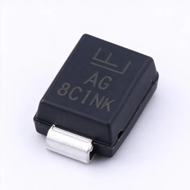
SMBJ6.0CA - 600W 6V Bi-Dir TVS Diode | Littelfuse | Surge
The Littelfuse SMBJ6.0CA is a 600 W bi-directional surface-mount transient voltage suppressor (TVS) diode with a 6.0 V reverse stand-off voltage, 6.67 V breakdown voltage, and 10.3 V maximum clamping voltage at 58.3 A peak pulse current, housed in the DO-214AA (SMBJ) package. A TVS diode is a clamping overvoltage-protection device that responds to transient events in picoseconds, diverting surge current away from sensitive ICs. Within the power-electronics hierarchy, the TVS diode sits under surge protectors and voltage references in the broader family of circuit-protection components, complementing fuses and varistors in a layered protection scheme. Key features of the SMBJ6.0CA include a 600 W peak pulse power rating (10/1000 us waveform per the SMBJ family datasheet), glass-passivated chip construction for low leakage current, and a bi-directional configuration (the C suffix) that clamps transients of both polarities - ideal for AC lines and bidirectional signal interfaces. The package supports surface-mount reflow assembly on standard land patterns. The device protects against voltage transients induced by inductive load switching and lightning per the Littelfuse SMBJ series datasheet, and the ST SMBJ series variant is designed for ESD protection per IEC 61000-4-2 and MIL STD 883 Method 3015. Response time is at the nanosecond level, making it effective against fast-rising ESD and switching spikes that slower varistors cannot catch. Typical applications include protection of I/O interfaces, VCC power buses, 5V and 3.3V logic rails, automotive inductive-load switching nodes, and industrial control equipment. Placing the SMBJ6.0CA directly across the rail to be protected clamps surges before downstream ICs see destructive voltage levels. Design tip: choose a stand-off voltage at or above the maximum continuous operating voltage of the rail - at 6.0 V stand-off, the SMBJ6.0CA suits 5V logic rails with margin, while its leakage current remains low at normal operating voltage. This page synthesizes distributor pricing, verified drop-in alternatives from Littelfuse, STMicroelectronics, Diodes Incorporated, Microchip and Yangjie, plus practical design notes not found in a single manufacturer datasheet.

SMBT2907AE6327HTSA1 - 60V 600mA PNP BJT | Infineon
Infineon Technologies SMBT2907AE6327HTSA1 is a general-purpose PNP bipolar junction transistor rated for 60 V collector-emitter voltage, 600 mA collector current, and 200 MHz transition frequency, with 330 mW device power in a three-pin SOT-23 surface-mount package. The automotive-qualified ordering code is associated with AEC-Q101 qualification, and the Pb-free package is identified as RoHS compliant in the retrieved manufacturer-family data. A bipolar junction transistor, or BJT, is a three-terminal semiconductor device that uses charge carriers to control current between a collector and emitter. In a PNP transistor, the emitter is normally biased above the base, and the collector current is controlled by base drive. The BJT belongs to the transistor hierarchy, which also includes NPN devices, and is widely used for switching, amplification, level translation, biasing, and driver stages. The SMBT2907A family provides low collector-emitter saturation voltage, a characteristic explicitly identified in the retrieved Infineon data. Its 60 V voltage rating supports higher-voltage control and switching circuits than lower-voltage general-purpose transistors, while the 200 MHz transition frequency supports faster switching behavior. The 600 mA collector-current and 330 mW power figures define the headline electrical limits used when selecting the part. The device is suitable for low- and medium-frequency signal stages, transistor-switched loads, bias networks, and complementary switching arrangements. In automotive and industrial systems, the AEC-Q101 qualification designation can simplify qualification work when the exact ordering variant and all operating requirements are acceptable. The SOT-23 footprint also supports compact PCB layouts, although correct pin orientation is essential because the emitter, base, and collector functions are not interchangeable. Designers should verify the maximum ratings, DC current, power dissipation, thermal conditions, and switching behavior against the manufacturer datasheet before applying the device as a direct replacement. Base current must be sufficient to keep the transistor in the intended operating region; otherwise, saturation voltage and switching performance may suffer. The retrieved data does not provide verified pricing tiers, so commercial values are represented by the required data-needed markers rather than guessed. This page combines verified manufacturer-family specifications, distributor listings, cross-reference evidence, package details, application guidance, and engineering selection notes to provide a practical reference for engineers evaluating this PNP transistor.
SMCJ33A - 1500W 33V Uni-Directional TVS Diode | Littelfuse
The Littelfuse SMCJ33A is a 1500W peak-pulse-power unidirectional Transient Voltage Suppressor (TVS) diode rated at 33V working standoff voltage, supplied in the industry-standard DO-214AB (SMC) surface-mount package. The device clamps at 53.3V maximum and absorbs up to 28.2A of peak pulse current (Ipp) on a 10/1000µs waveform, providing robust secondary protection against lightning-induced transients, inductive load switching, and ESD events on DC power rails and signal lines. A TVS diode is a solid-state avalanche device engineered to remain non-conductive at normal circuit voltages and to conduct sharply above its breakdown threshold, shunting transient energy away from sensitive downstream components. The 1500W SMCJ family belongs to the broader class of voltage-clamp suppressors, which sit between linear regulators and Zener diodes in a power-tree-of-compromise breakdown hierarchy. SMCJ parts are the 1500W successors to the older 600W SMBJ and 400W SMAJ series, sharing identical DO-214 family footprints but offering 2.5x to 3.7x higher surge handling. Key features include a glass-passivated die for stable leakage characteristics, low incremental surge resistance, fast response time of less than 1 ps from 0 V to Vbr minimum, and a low profile suitable for pick-and-place assembly. The DO-214AB package provides a flat heatslug and built-in strain relief that improves board-level reliability under thermal cycling. The Littelfuse variant is halogen-free and RoHS compliant, with a typical reverse leakage below 1 µA at the working voltage. The SMCJ33A uses a uni-directional avalanche junction fabricated in a single-polarity die construction. Because the device is uni-directional it must be oriented correctly with the cathode connected to the protected node, otherwise forward conduction will occur on negative transients. The 33V standoff is the optimal match for 24V industrial buses (with ±20% tolerance) and 28V avionics rails, clamping before downstream components reach their 40-50V absolute-maximum ratings. Typical applications include 24V industrial PLC input protection, telecom equipment -48V rectifier side protection (paired with a bidirectional part), automotive 24V truck body controller protection, RS-485/Profibus transceiver protection, and PoE port protection on the secondary side. The DO-214AB footprint allows reuse of existing land patterns designed for the SMCJ series. The wide operating temperature range of -55°C to +150°C supports both outdoor industrial and under-hood automotive deployments. When designing with the SMCJ33A, observe maximum lead soldering temperature, and place the device as close as possible to the input terminal or connector to minimize parasitic inductance in the protected loop. For applications exposed to negative surges, select the SMCJ33CA bidirectional variant instead. This page synthesizes distributor pricing, drop-in alternatives, and practical design notes not found in the manufacturer datasheet.
SMCJ33A-AT - 1500W 33V Uni-Directional TVS | DO-214AB
The SMCJ33A-AT is a 1500 W uni-directional surface-mount transient voltage suppressor (TVS) diode housed in a DO-214AB (SMC) package, designed to clamp voltage transients on power and signal lines. It features a working standoff voltage of 33 V, a minimum breakdown voltage of 36.7 V, and a maximum clamping voltage of 53.3 V at the 28.2 A peak pulse current (Ipp), with a peak pulse power rating of 1500 W for a 10/1000 µs waveform. The device is uni-directional (A-suffix), making it suitable for DC bus protection where only positive transients are of concern. A Transient Voltage Suppressor (TVS) diode is a clamping semiconductor device that diverts destructive transient energy away from sensitive downstream circuitry. When the line voltage exceeds the breakdown threshold, the TVS transitions from a high-impedance state to a low-impedance avalanche mode within picoseconds, shunting surge current to ground and clamping the voltage to a safe level. The DO-214AB (SMC) package family is the 1500 W workhorse of the TVS market, sitting in the hierarchy: TVS diode → ESD/transient protection → discrete semiconductor → circuit protection component. Key features of the SMCJ33A-AT include a fast response time of typically less than 1 ps from 0 V to VBR(min), glass-passivated junction construction for stable leakage and long-term reliability, a low-profile body for compact board layouts, built-in strain relief for robust surface-mount soldering, and excellent clamping capability per IEC 61000-4-2 (ESD) and IEC 61000-4-4/5 (EFT/surge) guidelines. The repetitive duty cycle is rated at 0.05%, with typical reverse leakage under 1 µA at the working voltage. The SMCJ33A-AT is widely used for secondary protection of 24 V industrial buses, automotive 12 V/24 V load-dump suppression, telecom -48 V rectifier output rails, and protection of DC/DC converter inputs from inductive kickback. It also appears in USB Type-C PD, RS-485/RS-232 transceiver protection, and surveillance/PoE line-card protection circuits. When designing with the SMCJ33A-AT, confirm that the system's maximum continuous working voltage never exceeds 33 V, and that the PCB land pattern follows the DO-214AB (SMC) recommendations. Note that for bidirectional requirements (positive and negative transients) the SMCJ33CA variant should be selected instead. This page consolidates verified distributor pricing (as of 2026-10-05), DO-214AB drop-in alternatives from multiple TVS manufacturers, and design guidance not found in any single manufacturer datasheet — enabling engineers to qualify second sources and reduce BOM risk.
SMCJ33A-AT-TR13 - 1500W 33V TVS Diode | YAGEO | DO-214AB
The YAGEO SMCJ33A-AT-TR13 is a 1500W peak-pulse-power unidirectional transient voltage suppressor (TVS) diode in an automotive-grade-qualified SMC (DO-214AB) surface-mount package. It features a 33V working standoff voltage (VWM), 36.7V minimum breakdown voltage, and a maximum clamping voltage of 53.3V at 28.2A peak pulse current (IPP). The -AT suffix denotes AEC-Q101 automotive qualification, and TR13 specifies 13-inch tape-and-reel packaging. The DO-214AB (SMC) package provides a robust footprint for high-power transient suppression in automotive and industrial environments. A TVS diode (transient voltage suppressor) is a discrete semiconductor designed to clamp voltage spikes and divert surge energy away from sensitive downstream circuitry. TVS diodes sit in the broader protection taxonomy alongside MOVs (metal-oxide varistors), Zener diodes used for clamping, and gas-discharge tubes; the TVS is differentiated by its sub-nanosecond response time and precise clamping voltage. The SMCJ series occupies the high-energy tier of TVS products, between smaller SMA-packaged parts (400W) and larger SMD packages such as SMCJ/SMDJ (1500W/3000W), serving as a key building block in the surge-protection hierarchy of power-management and circuit-protection subsystems. Key features include 1500W peak pulse power dissipation at a 10/1000µs waveform, glass-passivated die construction for stable breakdown characteristics, and a low leakage current of typically 1µA at the working voltage. The diode offers unidirectional clamping polarity (A suffix), excellent clamping capability, fast response time (typically <1 ns), and RoHS-compliant, halogen-free termination finish. The -AT variant adds automotive-grade reliability screening per AEC-Q101, making it suitable for under-the-hood and chassis electronics. Technically, the SMCJ33A-AT uses a silicon avalanche-junction structure that conducts in reverse breakdown when the applied voltage exceeds the breakdown threshold. At the 53.3V clamping voltage, the device can sink up to 28.2A for a brief pulse without failing, diverting energy that would otherwise damage downstream ICs. The peak pulse power is rated for a 10/1000µs exponential waveform per IEC 61000-4-2 and similar surge standards. Steady-state power dissipation is limited to 5W on a standard FR-4 PCB with adequate copper. Typical applications include 24V automotive load-dump protection (ISO 7637-2), CAN/LIN bus transceiver protection, industrial PLC I/O surge protection, USB and HDMI port ESD suppression on automotive infotainment, and protection of DC-DC converter input rails from inductive load transients. The wide 33V standoff is also useful in 24V industrial bus systems and battery-management protection circuits. When designing with this device, observe the derating of peak pulse power with pulse duration and temperature - the 1500W rating is at 25°C and a 10/1000µs waveform; shorter pulses and lower temperatures give higher ratings. Place the TVS as close as possible to the connector or entry point where transients enter the PCB, with wide, short traces to minimize parasitic inductance. The junction temperature should not exceed 150°C under any operating condition, including during surge events. This page synthesizes distributor pricing, drop-in alternatives, and practical design notes for the SMCJ33A-AT-TR13 that complement the manufacturer datasheet.
SMCJ33A-E - 1500W 33V Uni-Directional TVS Diode DO-214AB | Littelfuse
The Littelfuse SMCJ33A-E is a 1500 W peak-pulse-power uni-directional transient voltage suppressor (TVS) housed in a surface-mount DO-214AB (SMC) package with standoff voltage of 33 V and 5 % tolerance. It clamps at 53.3 V typical with a peak pulse current of 28.2 A (8/20 µs), providing robust suppression of inductive transients, ESD, and lightning-induced surges on power and data lines. A transient voltage suppressor (TVS) is a clamping semiconductor device designed to protect sensitive downstream electronics by limiting overvoltage transients to a controlled clamp voltage. In the system protection hierarchy, TVS diodes sit at the first line of defense, ahead of series PTCs/fuses, and downstream of common-mode chokes. They combine sub-nanosecond response time with high peak-current handling, making them ideal for IEC 61000-4-2 ESD, IEC 61000-4-4 EFT, and IEC 61000-4-5 surge events on industrial, automotive, and telecom interfaces. Key features include a 1500 W peak pulse power rating (10/1000 µs waveform), a maximum clamping voltage of 53.3 V at 28.2 A Ipp, a minimum breakdown voltage of 36.7 V, and a maximum leakage current on the order of 1 µA at standoff. The DO-214AB (SMC) package provides a compact, low-profile surface-mount footprint with gull-wing leads that support visual solder-joint inspection, and the -E suffix designates a 13-inch tape-and-reel (TR13) packaging variant per Littelfuse ordering nomenclature. The SMCJ33A-E uses a uni-directional avalanche junction architecture; its breakdown characteristic is asymmetric, clamping positive transients only. The device is constructed with a glass-passivated die that delivers stable Vbr across temperature and long-term reliability. Its thermal performance allows operation across -55 °C to +150 °C Tj, and the SMC package's thermal resistance of approximately 30 °C/W on a standard JEDEC FR-4 board supports repetitive surge events without derating. The SM-JT550 family also meets moisture sensitivity level 1 (MSL1) per JEDEC J-STD-020, simplifying storage and board-level handling. Typical applications include 24 V industrial bus protection (RS-485, CAN, Profibus), DC power-rail transient suppression in telecom equipment, secondary protection behind telecom line drivers, USB and HDMI port protection, and automotive load-dump protection up to 35 V continuous. Designers commonly place the SMCJ33A-E on 24 V supply rails and signal lines exposed to outdoor or industrial transients. Unlike polymer PTCs or MOVs, TVS diodes offer fast, repeatable, sub-nanosecond response and tight clamp-voltage tolerance. When designing with this device, ensure the clamping voltage stays below the absolute maximum rating of downstream ICs. Place the TVS diode as close as possible to the connector entry point and use a low-inductance ground return; keep the PCB trace between the protected line and the TVS anode shorter than 5 mm. This page synthesizes pricing across major distributors, drop-in alternatives, and practical design notes not found in the bare datasheet.
SMCJ45A-E3/57T - 1500W TVS Diode, 45V Standoff, Uni-Directional | Vishay
The Vishay General Semiconductor SMCJ45A-E3/57T is a 1500 W peak-pulse-power unidirectional Transient Voltage Suppressor (TVS) housed in the surface-mount DO-214AB (SMC) package. It provides a 45 V reverse-standoff voltage, a minimum breakdown voltage of 50 V, a maximum clamping voltage of 72.7 V, and a peak-pulse current rating of 20.6 A on a 10/1000 µs waveform. The /57T suffix designates the part for Tape-and-Reel packaging (850 pcs per 7" reel). The part belongs to Vishay's TransZorb SMCJ series (SMCJ5.0A through SMCJ188CA). A Transient Voltage Suppressor (TVS) is a semiconductor protection device designed to clamp fast over-voltage transients (ESD, lightning, inductive load switching) to a safe level, thereby protecting downstream components. TVS diodes operate in the avalanche-breakdown mode when the applied voltage exceeds their breakdown voltage, shunting transient current away from the protected circuit. The TVS belongs to the broader circuit-protection category alongside varistors (MOVs), surge protectors, and PTC resettable fuses, and sits below voltage regulators and power MOSFETs in the power-management hierarchy. Key features include a glass-passivated chip junction for long-term reliability, low-profile DO-214AB (SMC) package ideal for automated placement, uni-directional polarity, built-in strain relief, low inductance, excellent clamping capability, fast response time (typically < 1 ps from 0 V to BV min), low reverse leakage at standoff, and a repetition-rate (duty cycle) of 0.05%. The series is RoHS compliant and lead-free. Technically, the 1500 W P_PPM is measured at a 10/1000 µs exponential waveform per IEC 61000-4-5 / IEEE C62.41 surge standards. The DO-214AB (SMC) package has a typical thermal resistance of approximately 50 °C/W junction-to-ambient on a standard JEDEC test board, which is important when calculating steady-state power dissipation under repetitive surges. Typical applications include DC power-line protection on 24 V industrial buses, automotive load-dump protection (with appropriate derating), telecom equipment surge protection, USB / HDMI port protection, and protection of microcontroller I/O pins in industrial PLCs. In all these use cases the 45 V standoff aligns with 24 V rails and 28 V avionics rails. For higher-voltage systems the SMCJ series includes variants up to 170 V standoff in the same footprint. Design consideration: derate peak-pulse power for non-standard pulse widths. The 1500 W rating is specified on a 10/1000 µs waveform; shorter pulses (e.g. 8/20 µs lightning surges) must use the device's pulse-power curve, and longer pulses (e.g. 10/100 ms load-dump) must use the load-dump curve with substantially lower P_PPM. Always refer to the published derating curves in the manufacturer datasheet. This page synthesizes distributor pricing, drop-in pin-equivalent alternatives, and practical surge-protection design notes not found in the manufacturer datasheet.
SMMBTA56LT1G - 80V PNP Driver BJT 500mA | onsemi SOT-23
The onsemi SMMBTA56LT1G is a PNP silicon bipolar junction transistor (BJT) designed for linear and switching driver applications, rated at 80V VCEO, 500mA continuous collector current, and 225mW power dissipation in a SOT-23-3 (TO-236) surface-mount package. It features 50MHz transition frequency, PNP polarity for high-side switching or low-side load-driving roles, and is qualified to AEC-Q101 standards for automotive and other demanding environments. A bipolar junction transistor (BJT) is a three-terminal semiconductor device consisting of an emitter, base, and collector, in which a small base current controls a much larger collector current. The PNP variant conducts when the base is pulled below the emitter, enabling low-side switching of loads tied to a positive rail. BJTs sit in the broader taxonomy: PNP transistor -> BJT -> bipolar device -> discrete semiconductor. They remain preferred over MOSFETs for low-cost analog amplification, saturation-mode switching, and high-current linear regulation where their current-handling per unit area is favorable. Key differentiating specifications: 80V collector-emitter breakdown gives wide margin above 24V industrial rails; 500mA continuous collector current handles relays, solenoids, and LED strings; 50MHz transition frequency supports medium-speed switching such as PWM audio or low-frequency SMPS drivers; and SOT-23-3 footprint enables compact PCB designs. The 225mW power dissipation requires thermal management via copper pours rather than large heatsinks. Technically, the SMMBTA56LT1G uses an epitaxial planar construction with the S-prefix marking indicating onsemi's automotive-grade qualification (AEC-Q101) and PPAP capability, distinct from the MMBTA56 series. The device is Pb-Free, Halogen Free/BFR Free, and RoHS compliant, with MSL 1 moisture sensitivity enabling unlimited floor-life storage. Typical applications include automotive load drivers (relays, lamps, solenoids), industrial control switching, linear amplifiers, MOSFET gate drivers, level shifters, and general-purpose switching circuits where compact SOT-23 packaging and automotive-grade reliability are required. Compared to its MMBTA56 predecessor, the SMMBTA56LT1G adds AEC-Q101 qualification and PPAP support. A key design consideration: PNP transistors at 500mA in SOT-23 typically require thermal relief - at full load the 225mW dissipation can push junction temperature near limits, so designers should allocate copper area or limit continuous duty cycle. This part is intended for low-power surface mount applications where its SOT-23 footprint is acceptable. This page synthesizes distributor pricing, drop-in alternatives, and practical design notes not found in the manufacturer datasheet, giving engineers a single source for parametric comparison, sourcing decisions, and PCB layout guidance.

SP720ABTG - 14-Input 30V ESD TVS Array | Littelfuse
The Littelfuse SP720ABTG is a 14-input mixed-technology TVS diode array designed for electrostatic-discharge and over-voltage protection of sensitive external signal or bus lines. The device provides a listed 30 V rating, 1 A protection rating, 3 pF capacitance, and a 16-pin SOIC package. According to Littelfuse, each input uses two SCR/diode bipolar protection structures, while pins 1-7 and 9-15 are protected inputs and pin 8 provides the V+ or V- protection reference. A TVS diode array is a circuit-protection device that diverts transient current to a supply or ground rail while limiting voltage at a sensitive interface. The SP720 belongs to the transient-voltage-suppressor, mixed-technology, ESD-protection, and circuit-protection hierarchy. It is intended for systems in which exposed conductors or connectors can receive electrostatic discharge before reaching a protected logic, data, control, or communication circuit. The verified product data identifies 14 protection circuits in a surface-mount 16-SOIC package. Its 3 pF capacitance is particularly relevant to high-speed interfaces because parasitic capacitance can reduce signal rise time and disturb data timing. The 30 V and 1 A values characterize the protection device for design selection, but engineers should verify the complete datasheet limits, pulse conditions, and application configuration before relying on any rating. The SP720 architecture uses fast SCR structures together with diode protection paths. Littelfuse positions this family for general-purpose logic protection, data-bus protection, industrial process equipment, and systems requiring transient protection across many external lines. The array consolidates fourteen protected inputs into one package, reducing the number of discrete protection devices required when many connector pins need common ESD handling. Typical applications include industrial control interfaces, communication ports, instrumentation, data acquisition, embedded systems, and general-purpose connector protection. Protection is most effective when the protected traces are routed close to the connector, the array is connected to the appropriate supply or ground reference, and the signal integrity budget accounts for the array's capacitance. The part should not be treated as a substitute for surge-protection coordination outside the transient conditions covered by its manufacturer documentation. Designers should compare capacitance, protected-line count, voltage limits, current ratings, package dimensions, and exact pin mapping against the protected interface. For a data bus, the 3 pF capacitance must be checked against edge rate and receiver timing. For industrial equipment, the manufacturer’s IEC electromagnetic-compatibility guidance should be reviewed, while the exact applicable standard, system test level, and installation conditions remain design-specific and are not established by the supplied snippets. This page consolidates the verified manufacturer and distributor information, distinguishes the 14-input protection architecture from generic discrete TVS diodes, and provides practical selection and placement guidance. It does not infer unprovided production tolerances, temperature grades, surge endurance, or cross-manufacturer pin compatibility.
SP720ABTG-L - 14-Input ESD TVS Array | Littelfuse
The Littelfuse SP720ABTG-L is a 14-input transient-voltage-suppressor diode array for electrostatic-discharge and over-voltage protection of sensitive logic and data-bus circuits. The device is packaged in a surface-mount 16-SOIC and is identified as a lead-free/green SP720-series protection product. What is a TVS diode array? A TVS diode array is a semiconductor protection component placed between an external signal or bus line and sensitive circuitry. It diverts transient current away from the protected device while allowing normal low-voltage logic signals to pass. The SP720 family uses SCR/diode bipolar protection structures, with two structures associated with each input according to the Littelfuse datasheet. The verified product information identifies 14 available input-protection channels, surface mounting, and a 16-SOIC package. A distributor listing describes the related SP720ABTG variant as a mixed-technology TVS device with 14 circuits and a 16-SOIC package. The SP720ABTG-L ordering suffix is treated as the specified Littelfuse variant; electrical details beyond the supplied verified values are not independently expanded here. SP720 protection is appropriate for general-purpose logic protection, data buses, communication interfaces, and other exposed external lines where ESD transients can enter through connectors or cables. The array format provides centralized protection in one package, reducing the number of individual discrete protection devices required when several lines need protection. Placement close to the board entry point or connector is important because the protective device must intercept the transient before it propagates into the protected logic. Trace geometry, return paths, grounding, and the choice between the array and a discrete low-capacitance solution should be checked against the signal speed and operating requirements. This page combines the verified Littelfuse and distributor information with practical placement guidance and clearly marks unavailable specifications. Review the manufacturer datasheet and application note AN9734 before production release, especially for system-level ESD validation, signal integrity, and the exact electrical limits of the ordered suffix.

SPP11N80C3XKSA1 - 800V 11A CoolMOS C3 N-Channel MOSFET | Infineon
The Infineon SPP11N80C3XKSA1 is an N-Channel 800 V CoolMOS C3 power MOSFET delivering 11 A continuous drain current (Tc) and 156 W power dissipation (Tc) in a PG-TO220-3-1 through-hole package. Built on Infineon's revolutionary high-voltage CoolMOS C3 superjunction technology, it combines ultra-low effective output capacitance, ultra-low gate charge, and extreme dv/dt ruggedness, qualifying it for high-density switched-mode power conversion stages. A power MOSFET is a voltage-controlled three-terminal semiconductor switch (gate, drain, source) that converts DC or pulsed drive into a low-resistance conduction path between drain and source. The 800 V drain-source breakdown (V(BR)DSS) places this device in the high-voltage MOSFET class used in offline SMPS front ends, while the 11 A continuous rating places it in the mid-power segment, suitable for PFC stages, primary-side switches in flyback/forward converters, and industrial welding and motor-drive inverters. Hypernyms: power MOSFET -> MOSFET -> discrete semiconductor -> power semiconductor -> semiconductor. Synonyms: N-FET, N-channel enhancement-mode MOSFET, superjunction MOSFET, CoolMOS. Key features include 800 V drain-source breakdown (V(BR)DSS), 11 A continuous drain current at case temperature (ID @ Tc), 156 W maximum power dissipation (Ptot @ Tc), ultra-low gate charge (Qg) for reduced driver loss, ultra-low effective output capacitance (Coss(eff)) for higher switching frequency, high peak current capability for inductive loads, and extreme dv/dt rating for hard-switched topologies. The PG-TO220-3-1 package provides a low thermal-resistance path through the central mounting tab. Technically, CoolMOS C3 uses a vertical superjunction (SJ) structure that breaks the silicon area-resistance tradeoff of planar MOSFETs. The result is an order-of-magnitude lower specific on-resistance (RDS(on) x area) at the same voltage class. The trade-off is a non-linear Coss that decreases with VDS, which benefits zero-voltage-switching (ZVS) topologies like LLC and PFC boost. Pb-free lead plating and RoHS compliance support modern manufacturing directives, and JEDEC qualification assures reliability under industrial thermal and humidity stress. Typical applications include switch-mode power supplies (SMPS) for industrial 380-400 V AC-DC front ends, power factor correction (PFC) boost stages, telecom rectifier modules, solar inverter primary switches, induction-heating resonant half-bridges, and welding inverter power stages. The wide safety margin of an 800 V rating on a 230/400 V AC mains-rectified bus (peak ~565 V) gives designers additional headroom for surge and ring transients. When designing with this device, observe avalanche energy (EAS) limits during inductive turn-off, and add a low-impedance gate-drive loop to control dv/dt. For hard-switched topologies above 50 kHz, plan thermal dissipation carefully - the 156 W rating assumes a 25 C case temperature, and real PCB heatsinking typically derates this to 60-80 W. This page synthesizes distributor pricing, drop-in CoolMOS C3 alternatives, and practical design notes not found in the manufacturer datasheet alone.

SPP17N80C3XKSA1 - 800V 17A CoolMOS C3 MOSFET | Infineon
The Infineon SPP17N80C3XKSA1 is an 800 V, 17 A N-channel power MOSFET from Infineon's third-generation CoolMOS C3 family, housed in a through-hole PG-TO220-3-1 package with continuous drain current of 17 A at Tc and maximum power dissipation of 208 W at Tc. Built on Infineon's superjunction (SJ) technology platform introduced in 2001, it targets high-voltage switched-mode power supplies and industrial converters requiring low conduction and switching losses. A power MOSFET is a voltage-controlled semiconductor switch in which the gate field modulates a conduction channel between source and drain. Within the broader taxonomy, MOSFETs belong to discrete transistors, which sit under discrete semiconductors alongside diodes and thyristors; the CoolMOS superjunction family is a specialized MOSFET sub-family optimized for high breakdown voltages with markedly lower specific on-resistance (RDS(on) x area) than conventional planar MOSFETs. The C3 generation specifically reduces gate charge, output capacitance, and reverse-recovery charge relative to C2, enabling higher switching frequencies and smaller magnetics in offline SMPS designs. Key features of the SPP17N80C3XKSA1 include an 800 V drain-source breakdown voltage, 17 A continuous drain current at 25 C case temperature, 208 W maximum power dissipation at Tc, low intrinsic drain-source on-resistance for the voltage rating, and fast body-diode behavior suitable for hard-switched bridge converters. The through-hole PG-TO220-3-1 package provides a robust mechanical footprint with a metal tab that can be bolted to a heatsink for thermal management. Typical applications include switch-mode power supplies (SMPS) for telecom and server AC-DC front-ends, uninterruptible power supplies (UPS), solar inverters, welding equipment, and high-voltage industrial drives. The CoolMOS C3 series is well known for rugged avalanche capability and high dv/dt immunity, making it suitable for hard-switched PFC and half-bridge topologies. When designing with this part, ensure the gate driver delivers at least 10 V Vgs for full enhancement and that snubber or RCD protection is considered for hard-switched bridge circuits. Heatsink selection must account for the 208 W power rating and thermal resistance of the TO-220 package. This page synthesizes distributor pricing from DigiKey/Mouser/LCSC, drop-in TO-220-3 equivalents, and practical design notes not consolidated in the manufacturer datasheet. All specifications are anchored to the Infineon SPA/SPP 17N80C3 datasheet and the CoolMOS C3 product family documentation.

SPP80P06PHXKSA1 - P-Ch 60V 80A 340W TO-220 MOSFET | Infineon
The Infineon SPP80P06PHXKSA1 is a P-channel enhancement-mode power MOSFET rated at -60 V VDS and -80 A continuous drain current (at TC), with a maximum power dissipation of 340 W (TC), housed in a through-hole PG-TO220-3-1 (TO-220-3) package. Built on Infineon's mature OptiMOS P-channel silicon process, this part targets high-current switching on the high-side of a load (low-side switching with source tied to ground is also supported), replacing PNP bipolar transistors and P-channel MOSFETs from older process generations. A P-channel MOSFET (PMOS) is a voltage-controlled field-effect transistor in which the channel is formed by holes; turning the gate ON requires pulling the gate voltage below the source by at least the threshold voltage VGS(th), which simplifies high-side drive circuits because no charge pump or bootstrap is needed when the source is tied to the supply rail. P-channel MOSFETs sit inside the broader power MOSFET taxonomy (P-channel/N-channel, enhancement-mode/depletion-mode, planar/trench), which in turn belongs to the discrete power semiconductor family (MOSFET -> transistor -> discrete semiconductor -> power management component). Key features include a low on-state resistance for the voltage class, avalanche-rated single-pulse robustness, an operating junction temperature range of -55 C to +175 C, and a TO-220-3 through-hole footprint with a metal tab that doubles as the drain connection and a thermal mounting surface. The package accepts standard M3 screws and clip-on heatsinks, enabling straightforward thermal management in motor-drive, battery-protection, and power-ORing circuits. Internally, the device uses a trench-cell structure that minimizes RDS(on) per unit silicon area while keeping gate charge Qg low, so a logic-level gate driver can switch the part at moderate PWM frequencies without excessive driver loss. The body diode supports inductive commutation, simplifying half-bridge and flyback topologies. Compared with an equivalent N-channel MOSFET, this P-channel part eliminates the bootstrap/charge-pump network required for high-side switching, reducing BOM cost and PCB area at the expense of slightly higher RDS(on) at a given die size. Typical applications include high-side load switching in 12 V / 24 V automotive and industrial systems, reverse-battery protection, DC motor reverse-polarity switching, power-ORing between redundant supplies, USB Type-C VBUS hot-swap switches, and battery management systems (BMS) charge/discharge FETs. The P-channel polarity is particularly attractive when the load sits on the low side and the supply must be switched. When designing with this device, ensure the gate drive pulls below the source by at least 10 V to fully enhance the channel and minimize conduction loss. The metal tab must be mechanically fastened to a heatsink or copper pour with thermal interface material, because at -80 A the part dissipates substantial heat even at low RDS(on). This page synthesizes distributor pricing as of 2026-09-14, drop-in TO-220-3 alternatives from the Infineon OptiMOS P-channel family, and practical design notes that complement the manufacturer datasheet rather than restate it.

SPSB100G - 100A Power Semiconductor Module | [Brand]
The SPSB100G is a high-current power semiconductor module designed for demanding industrial and automotive power conversion applications. It delivers a continuous current rating of 100A and is housed in a robust module package suitable for chassis mounting. The module integrates advanced semiconductor technology to provide low conduction and switching losses, ensuring high efficiency in power stages. A power semiconductor module is a packaged assembly of multiple power semiconductor devices, such as IGBTs, MOSFETs, or diodes, configured in a specific topology (e.g., half-bridge, full-bridge, or three-phase) to handle high voltage and current levels. These modules are the building blocks of modern power electronics systems, converting and controlling electrical energy in applications ranging from motor drives to renewable energy inverters. They sit at the top of the power hierarchy, bridging raw power sources and the controlled loads that require precise energy management. Key features of the SPSB100G include a 100A continuous collector current, a collector-emitter voltage rating of [DATA_NEEDED: V_CES], and a low saturation voltage that minimizes conduction losses. The module also offers fast switching speeds, reducing switching losses and enabling higher frequency operation. Its isolated baseplate ensures safe heat dissipation and simplifies system integration, while the integrated temperature sensor provides real-time thermal monitoring for enhanced reliability. Technically, the SPSB100G leverages a trench-gate field-stop IGBT structure, which balances low on-state voltage drop with fast switching characteristics. The freewheeling diode is co-packaged with the IGBT, featuring soft-recovery behavior to reduce electromagnetic interference (EMI) and improve overall system performance. The module's internal layout is optimized for low parasitic inductance, which is critical for high-current, high-speed switching applications. Typical applications include industrial motor drives, uninterruptible power supplies (UPS), solar inverters, and electric vehicle (EV) traction inverters. In motor drives, the SPSB100G's high current capability and robust thermal performance enable precise speed and torque control. In solar inverters, its high efficiency contributes to maximum energy harvest, while in EV traction inverters, it delivers the power density and reliability required for automotive-grade operation. When designing with the SPSB100G, ensure adequate gate drive voltage and current to achieve optimal switching performance. Proper thermal management, including a suitable heatsink and thermal interface material, is essential to maintain junction temperature within safe limits. Additionally, consider the module's internal inductance when designing the DC-link layout to minimize voltage overshoots during switching transients.

SPW47N60C3 - 650V 47A CoolMOS C3 Power MOSFET | Infineon
The Infineon SPW47N60C3 is a 650V, 47A N-channel power MOSFET from the CoolMOS C3 series, housed in a TO-247-3 through-hole package. As a third-generation high-voltage superjunction device, it delivers a low specific on-state resistance (RDS(on)*A) and very low energy storage in output capacitance (Eoss at 400V), making it a benchmark 600V-class switching transistor for SMPS and motor drive topologies. A CoolMOS power transistor is a superjunction MOSFET architecture in which alternating p-type columns in the drift region compensate the electric field, breaking the silicon limit of conventional planar MOSFETs. Within the power semiconductor hierarchy, superjunction MOSFETs sit between standard planar MOSFETs and emerging SiC/GaN wide-bandgap devices, offering the best cost-per-ampere figure of merit for 500-650V applications. Key features include a 650V drain-source breakdown (V(BR)DSS), 47A continuous drain current at Tc, a typical on-state resistance of approximately 70 mΩ, and a 415W maximum power dissipation rating. The C3 platform improves switching losses versus the C2 series and supports high-frequency operation. Built-in source-connected Kelvin source pin and low gate charge (Qg) reduce driver stress. The SPW47N60C3 is engineered into PFC boost stages, LLC half-bridge converters, and three-phase inverter bridges for industrial drives. Typical use cases include server/telecom SMPS primary-side switches, solar micro-inverters, induction-heating resonant tanks, and welding inverter modules where 600V-class switching at >100kHz is required. When designing with this part, observe the avalanche rating during turn-off transients and respect the TO-247-3 thermal envelope. Use a low-inductance gate-driver layout (Kelvin connection) and add a TVS or RC snubber for high-dV/dt conditions to keep ringing below the V(BR)DSS margin.
SQ2325ES-T1 - 150V P-Ch TrenchFET MOSFET | Vishay | SOT-23
The Vishay Siliconix SQ2325ES-T1 is an automotive-grade P-Channel TrenchFET power MOSFET rated 150 V VDS and 840 mA continuous drain current, housed in a SOT-23-3 (TO-236) surface-mount package. It is qualified to AEC-Q101 and tested for 100% Rg and UIS, targeting harsh-environment switching and load-management circuits. A P-Channel MOSFET is a voltage-controlled device in which a negative gate-source voltage (relative to the source) creates a conducting channel between drain and source. As a member of the TrenchFET family, the SQ2325ES-T1 uses a vertical trench-gate cell pitch (sub-micron) that dramatically reduces on-resistance per unit silicon area compared with legacy planar P-Channel devices. The P-Channel topology sits within the broader taxonomy of enhancement-mode MOSFETs, which themselves belong to the power-MOSFET category of discrete semiconductors used for switching and amplification in power management, motor drive, and analog signal-path applications. Key features of the SQ2325ES-T1 include: 150 V drain-source breakdown voltage (V(BR)DSS), 840 mA continuous drain current (ID) at TC, 3 W power dissipation (PD) at TC, and a typical SOT-23-3 (TO-236) footprint with the standard JEDEC pinout (Pin 1 Gate, Pin 2 Source, Pin 3 Drain). The TrenchFET Gen-IV-style process delivers low on-resistance for the voltage class, and the device is rated to operate across -55 C to +175 C junction temperature, matching automotive under-hood requirements. The -T1 suffix denotes 7-inch tape-and-reel packaging, while the -GE3 suffix denotes lead-free (Pb-free) and RoHS-compliant terminal finish. Typical applications for the SQ2325ES-T1 include high-side and low-side load switching in automotive body electronics (lighting, HVAC valves, mirror fold), battery protection and reverse-polarity blocking in 12 V/24 V systems, level-shifters and high-side drivers for MCU GPIO, hot-swap insertion circuits, and small-signal analog switches in instrumentation. Its 150 V rating provides substantial headroom over the 12 V and 24 V automotive buses, with ample margin for inductive load transients. Designers should keep in mind that the SOT-23-3 thermal pad is the drain terminal; PCB copper area connected to the drain pad is the primary heat-dissipation path. For continuous operation above ~500 mA, recommend at least 1 square inch of 2-oz copper on the drain pad to keep junction temperature within safe limits. This page consolidates distributor pricing, qualified drop-in alternatives, and engineering design guidance that augments the manufacturer datasheet.
SQ2325ES-T1_GE3 - P-Ch 150V 840mA AEC-Q101 MOSFET | Texas Instruments
The Vishay Siliconix SQ2325ES-T1_GE3 is an automotive-grade P-Channel TrenchFET power MOSFET rated at 150 V drain-to-source voltage, 840 mA continuous drain current (Tc), and 3 W power dissipation (Tc), housed in a SOT-23-3 (TO-236) surface-mount package. As part of Vishay's SQ automotive MOSFET family, it is AEC-Q101 qualified and 100 % tested for Rg (gate resistance) and UIS (unclamped inductive switching) ruggedness, ensuring reliable operation under harsh electrical and thermal stress. A P-Channel MOSFET is a type of field-effect transistor where the conducting channel is formed by holes rather than electrons; it is activated by pulling the gate voltage below the source potential. P-Channel devices belong to the broader MOSFET family, which sits under discrete semiconductors in power-management and load-switching hierarchies. They are commonly used for high-side switching because, when the gate is grounded, the device turns on and pulls the load to the negative rail, simplifying drive circuitry in systems with a positive supply. Key features include 150 V VDS breakdown voltage, 840 mA continuous drain current at 25 °C case temperature, low on-resistance typical of Vishay TrenchFET silicon, and halogen-free construction per IEC 61249-2-21. The SOT-23-3 footprint keeps board area to roughly 4 mm² while still providing sufficient thermal dissipation for low-to-moderate power switching. Gate threshold voltage is specified to drive directly from logic-level signals or simple microcontroller GPIO outputs, depending on variant. Architecturally, the SQ2325ES uses Vishay's TrenchFET® vertical trench-gate process, which reduces specific on-resistance (RDS(on) × area) by concentrating the channel along a vertical trench sidewall rather than on the wafer surface. This yields lower conduction losses per unit silicon area compared with older planar P-Channel processes. The AEC-Q101 qualification and 100 % UIS testing make the part especially suited to automotive load-dump and inductive-load environments. Typical applications include automotive load switching, high-side power management in 12 V / 24 V systems, reverse-battery protection, level shifting, and general low-power switching where a small-footprint P-Channel device is required. It can also serve as a power-ORing element or as a bootstrap switch in half-bridge driver circuits. When designing with this part, ensure that the gate-to-source voltage stays within the absolute maximum rating (typically ±20 V) and that switching losses are kept within the package's thermal limits. The SOT-23-3 package relies on the drain tab (pin 3) for primary heat dissipation, so adequate copper area on the drain pad is essential for thermal performance. This page synthesizes distributor pricing, AEC-Q101 qualification status, drop-in equivalents, and practical design notes that go beyond the manufacturer datasheet's spec table.