MOSFETs
Produtos (1294)

IRFB4410PBF - 100V N-Channel HEXFET MOSFET TO-220AB | Infineon
The Infineon IRFB4410PBF is a 100V single N-Channel HEXFET power MOSFET housed in a TO-220AB through-hole package, delivering a continuous drain current of 88A at 25°C case temperature and 200W of power dissipation. Built on Infineon's proprietary HEXFET technology, it achieves a typical on-resistance of 10 mOhm at VGS=10V and supports avalanche-rated switching with low gate charge of 120 nC. A HEXFET power MOSFET is a metal-oxide-semiconductor field-effect transistor built around a hexagonal cell layout that maximizes channel density per unit silicon area, lowering RDS(on) and improving switching efficiency compared to legacy planar MOSFETs. Within the broader power-semiconductor hierarchy, it sits below insulated-gate bipolar transistors (IGBTs) for higher voltage/current roles but above small-signal MOSFETs in current handling, and it belongs to the discrete-semiconductors > MOSFETs product family. Key features include fully avalanche-rated ruggedness, an improved gate structure for dynamic dV/dt immunity, fast intrinsic body diode with low reverse recovery, and a logic-level compatible 10V VGS(th) that simplifies gate drive from standard PWM controllers. The TO-220AB package provides a thermal resistance of 0.75 C/W junction-to-case, enabling high continuous dissipation when mounted to a small clip-on heatsink. This device is targeted at high-efficiency synchronous rectification in switch-mode power supplies, hard-switched and high-frequency circuits, uninterruptible power supplies (UPS), DC motor drives, and class-D audio amplifiers where low conduction loss and high peak current handling are required. Designers benefit from Infineon's well-known TO-220 family tooling, robust transient ruggedness, and broad second-source availability.

IRFB52N15DPBF - 150V 51A N-Channel HEXFET MOSFET | Infineon
The Infineon IRFB52N15DPBF is a 150V N-channel HEXFET power MOSFET rated for 51A continuous drain current (Tc) and 32mΩ maximum on-resistance, housed in a TO-220AB through-hole package. It combines low gate charge (60nC typical) with fully characterized capacitance including effective COSS, simplifying high-frequency DC-to-DC converter design and synchronous rectification layouts. A power MOSFET (Metal-Oxide-Semiconductor Field-Effect Transistor) is the dominant switching element in modern power electronics, sitting one level above BJTs in the switch-mode power conversion hierarchy. Within the MOSFET family, N-channel enhancement-mode devices like the IRFB52N15DPBF are the workhorses of high-side and low-side switching because their higher electron mobility yields lower RDS(on) per unit silicon area than equivalent P-channel parts. The HEXFET process is Infineon's (originally International Rectifier's) proprietary vertical DMOS cell architecture using a hexagonal cell geometry that maximises channel density per die. Key electrical specifications include a drain-source breakdown voltage (V(BR)DSS) of 150V, continuous drain current of 51A at 25°C case temperature, pulsed current capability up to roughly 200A, gate threshold voltage of 2V to 4V, and a maximum power dissipation of 230W at Tc. The 32mΩ RDS(on) at VGS=10V minimises conduction losses in high-current switching paths, while the 60nC typical gate charge enables fast switching transitions at frequencies above 100 kHz. This device targets high-frequency DC-DC converters, plasma display panels, uninterruptible power supplies, motor drive H-bridges, and solar inverters. The industrial-grade qualification standard (per IR/Infineon) supports harsh-environment deployment. Designers benefit from the device's avalanche-rated single-pulse capability and dv/dt ruggedness for snubber-less operation in half-bridge topologies. When designing with this MOSFET, careful attention to gate-drive voltage (10V recommended for full RDS(on) enhancement) and thermal management is essential - the TO-220AB can dissipate approximately 230W with adequate heatsinking. The body diode is suitable for freewheeling in bridge configurations but exhibits moderate reverse recovery, so for hard-switched bridges above 50 kHz consider an external SiC Schottky in parallel.
IRFB7437PBF - 40V 195A 2.0mΩ StrongIRFET N-MOSFET | Infineon
The Infineon IRFB7437PBF is a 40 V N-channel power MOSFET from Infineon's StrongIRFET family, delivering 195 A continuous drain current (Tc) and an ultra-low typical on-resistance of 1.5 mΩ (max 2.0 mΩ at VGS=10 V) in a TO-220AB through-hole package. According to the manufacturer datasheet, the part dissipates up to 230 W at Tc=25°C and is built on a silicon-limited die that supports transient drain currents up to 250 A. The 150 nC total gate charge and 49 nC Miller plateau charge enable high-frequency switching for motor control and synchronous rectification. A power MOSFET is a voltage-controlled semiconductor switch that uses the gate electric field to modulate conduction between drain and source. The IRFB7437PBF belongs to the N-channel enhancement-mode MOSFET family, a subtype of power transistors (hypernyms: MOSFET → field-effect transistor → transistor → discrete semiconductor). Its low R_DS(on) minimizes conduction loss, while the TO-220 through-hole package allows straightforward PCB mounting and direct attachment to an external heatsink for high-current applications. Key features include a -55°C to +175°C operating junction temperature range, an avalanche-rated body diode, and a logic-level VGS(th) that supports standard 10 V gate drive. The TO-220AB package provides a thermal resistance of approximately 0.62°C/W (junction-to-case), enabling the 230 W power rating. The part is also lead-free (PBF suffix indicates Pb-free plating) and fully RoHS compliant. The IRFB7437PBF uses Infineon's StrongIRFET trench cell technology, which optimizes the cell pitch and gate geometry for the lowest possible R_DS(on) × Qg figure of merit in the 40 V class. This makes the device competitive with discrete GaN FETs in cost-sensitive high-current applications while retaining the ruggedness and avalanche capability of silicon. According to the Infineon datasheet, the die supports a single-pulse avalanche energy rating and is fully characterized for linear-mode operation. Typical applications include brushed DC motor drives, BLDC motor drives, battery protection circuits, half-bridge and full-bridge topologies, synchronous rectification in DC/DC converters, resonant mode power supplies, OR-ing and redundant power switches, and DC/AC inverters. The 40 V rating suits 12 V and 24 V automotive/industrial buses, while the 195 A current rating supports high-power tools, e-bike controllers, and battery management systems. When designing with this device, ensure that VGS is driven to 10 V for full enhancement and that the gate driver can source/sink the 49 nC Miller charge within the required rise/fall time. The body diode has a slow reverse recovery; pair with an anti-parallel FET or Schottky if hard switching. A low-impedance Kelvin source connection (using TO-220 tab as source) is critical at high di/dt. This page synthesizes distributor pricing, drop-in TO-220AB alternatives, and practical thermal design notes not found in the manufacturer datasheet alone.
IRFB7534PBF - 60V 195A StrongIRFET N-Channel MOSFET | Infineon
The Infineon IRFB7534PBF is a 60 V N-channel power MOSFET in the StrongIRFET™ family, rated for 195 A continuous drain current (Tc) and 294 W power dissipation (Tc), housed in a through-hole TO-220AB package. It is optimized for low RDS(on) (2.4 mΩ max at VGS=10 V) and high inrush current capability, making it well-suited to brushed motor drive, BLDC motor drive, battery-powered circuits, and half-/full-bridge topologies. A power MOSFET is a voltage-controlled three-terminal switch that conducts current between drain and source when a sufficient gate-to-source voltage is applied. Within the broader taxonomy, the IRFB7534PBF sits at: N-channel MOSFET → power MOSFET → discrete semiconductor → power management building block. The TO-220AB package places it in the through-hole, single-die, three-pin family (TO-220 family → THT discrete semiconductor → JEDEC-recognized outline). The "PbF" suffix indicates lead-free (Pb-free) terminal finish compliant with RoHS. Key features include an ultra-low on-state resistance of 2.4 mΩ max, low gate charge for fast switching, an avalanche-rated body diode for unclamped inductive switching, and a logic-level-friendly threshold that drives cleanly from standard 10 V gate drive. The TO-220AB's metal tab doubles as a heatsink mount, and the device is qualified to MSL1 (unlimited floor life) for simplified handling. Built on Infineon's StrongIRFET™ planar process, the IRFB7534PBF balances low conduction loss with robust short-circuit-withstand capability. The 195 A continuous rating (case-referenced) is de-rated by PCB layout and heatsinking; designers must use the thermal resistance curve to size the heatsink for their specific load profile. Typical applications include brushed and BLDC motor drives, battery protection and switching, low-voltage DC-DC converter high-side switches, e-bike and power-tool controllers, and high-current load switches in 24 V/48 V industrial rails. When designing with this MOSFET, ensure the gate driver delivers at least 10 V VGS for full enhancement and consider a gate-source pull-down resistor (10 kΩ) to prevent inadvertent turn-on from Miller capacitance during high dV/dt events. This page synthesizes distributor pricing, drop-in alternatives, and practical design notes not found in the manufacturer datasheet, giving engineers a one-stop reference for part selection, sourcing, and PCB implementation.
IRFB7545PBF - 60V 95A N-Channel HEXFET MOSFET | Infineon
The Infineon IRFB7545PBF is an N-channel power MOSFET rated at 60 V VDS max, 95 A continuous drain current (Tc), and 125 W power dissipation (Tc), housed in a lead-free TO-220AB through-hole package. Built on Infineon's StrongIRFET™ trench technology, it delivers a maximum on-resistance of 5.9 mOhm at VGS = 10 V, optimized for low conduction loss in high-current switching applications. A power MOSFET (Metal-Oxide-Semiconductor Field-Effect Transistor) is a voltage-controlled semiconductor switch used in power electronics to switch and amplify DC/DC, DC/AC, and motor-drive circuits. The StrongIRFET™ family sits within the broader N-channel MOSFET hierarchy: MOSFET → power MOSFET → N-channel enhancement-mode → HEXFET/StrongIRFET → Infineon OptiMOS/StrongIRFET line. TO-220 remains one of the most widely used through-hole power packages because its metal tab doubles as both an electrical drain connection and a thermal path for an external heatsink. Key specifications include R_DS(on) max of 5.9 mOhm at 10 V VGS, VDS of 60 V, continuous ID of 95 A at Tc, pulsed current capability of 380 A, and avalanche-rated single-pulse current of 57 A. The thermal resistance junction-to-case (RthJC) is 1.0 C/W, allowing effective heat extraction with a modest clip-on heatsink. Gate threshold voltage is typically 3.5 V, supporting standard 10 V logic-level drive and providing sufficient margin for gate-drive induced ringing. The IRFB7545PBF is targeted at brushed motor drive applications, where its low R_DS(on) and high pulsed-current handling enable cooler operation and higher torque density. Additional uses include synchronous-rectifier secondary-side switches in sub-60 V DC/DC converters, high-current solenoid drivers, and OR-ing FETs in redundant 48 V telecom supplies where avalanche ruggedness is mandatory. Designers should size the heatsink to keep Tj below 125 C under worst-case continuous load, and route the gate drive with a series resistor of 10–33 ohm to suppress ringing. The TO-220 tab is electrically connected to the drain — a clearance of at least 2 mm between the tab and any grounded heatsink is required when an insulated pad is not used. This page synthesizes distributor stock, cross-reference alternatives, and application guidance not always visible on the manufacturer product page.

IRFH4253DTRPBF - 25V Dual N-Ch MOSFET, 1.45mΩ PQFN | Infineon
The Infineon IRFH4253DTRPBF is a 25 V dual N-channel MOSFET in a 5 mm x 6 mm PQFN (Power QFN) surface-mount package, integrating a low-charge control FET and a low-Rdson synchronous FET plus an intrinsic Schottky diode in a single die. The control MOSFET section is characterized by typical Qg of 31 nC, while the synchronous FET section delivers a typical on-resistance of 1.45 mΩ at 10 V VGS and supports continuous drain current up to 64 A (per MOSFET section, 25 °C), giving a combined package power dissipation of 31 W to 50 W depending on mounting and PCB copper area. A dual MOSFET (also called a half-bridge co-pack or asymmetric co-pack MOSFET) combines a high-side control FET and a low-side synchronous FET, or two synchronous FETs, in one thermally efficient PQFN. The co-pack approach shortens the high-current loop between the two FETs, reducing parasitic inductance, ringing, and switching losses versus two discrete MOSFETs - critical for high-frequency synchronous buck converters, point-of-load regulators, and OR-ing applications. The IRFH4253D targets point-of-load (POL) DC-DC conversion where small footprint, low Rdson, and integrated Schottky diode operation are required to maximize power density. Key features of the IRFH4253D include low charge on the control FET for fast switching, very low Rdson on the synchronous FET for reduced conduction loss, an integrated Schottky diode with low forward voltage to suppress body-diode reverse-recovery losses, and the PQFN 5x6 package which provides a low thermal resistance path from junction to PCB. The device is RoHS compliant, lead-free, and qualified to MSL1 moisture sensitivity, simplifying board-level reliability and assembly. The 'TRPBF' suffix indicates tape-and-reel packaging with a lead-free, Pb-free finish. Typical applications include synchronous buck converters in POL regulators, high-frequency DC-DC bricks, voltage regulator modules (VRMs), and OR-ing FETs for redundant power architectures. The dual-FET integration is especially useful in space-constrained telecom, server, and graphics card designs where two discrete SO-8 or smaller MOSFETs cannot match the combined Rdson, charge, and thermal performance of this co-pack. When designing with this part, follow the layout recommendations in the manufacturer datasheet to keep the high-current loop minimal, use sufficient copper pour on the PQFN thermal pad, and respect the maximum junction temperature of 150 °C. Because the device integrates an asymmetric pair plus a Schottky, it cannot be used as a generic dual N-channel - one section is optimized for switching speed and the other for conduction.
IRFH5015TRPBF - 150V N-Ch 31mOhm HEXFET MOSFET | Infineon
The Infineon IRFH5015TRPBF is a 150V N-channel power MOSFET built on IR HEXFET technology, housed in a SuperSO8 (5x6) surface-mount package with 8 pins. It delivers a maximum drain-source voltage (VDS) of 150V, continuous drain current of 10A at TA and 56A at TC, with a maximum on-resistance (RDS(on)) of 31 mOhm and total gate charge (Qg) of 33 nC. The device is optimized for 10V gate drive, which simplifies driver selection in standard half-bridge and synchronous-rectification topologies. What is a HEXFET power MOSFET? A HEXFET is Infineon's (originally International Rectifier's) brand name for a power MOSFET built on a hexagonal-cell vertical DMOS process, where each cell contains a hexagonal geometry that maximizes channel density per unit die area. HEXFET MOSFETs sit within the broader product hierarchy of: MOSFET -> power MOSFET -> discrete semiconductor -> N-channel enhancement-mode device. The IRFH5015 belongs to the medium-voltage N-channel family designed for switching power supply primary-side switches, motor drive H-bridges, and DC-DC converter high-side switches. Key features of the IRFH5015TRPBF include industry-standard SuperSO8 5x6 packaging, JEDEC-qualified reliability, low RDS(on) of 31 mOhm at VGS=10V, and a single N-channel configuration with built-in body diode. The Power-SO8 variant is pin-compatible with the standard SO-8 footprint used by many competing N-channel MOSFETs, enabling drop-in second-source opportunities in existing layouts. The product is qualified per JEDEC standard and optimized for broadest availability from distribution partners. Architecturally, the IRFH5015 uses a planar-cell N-channel enhancement-mode HEXFET structure. The die is rated for 3.6W continuous power dissipation at TA=25C, scaling to 156W at TC=25C. The combination of 150V breakdown, 33 nC Qg, and 31 mOhm RDS(on) places it in the sweet spot for 48V telecom bus converters, 24V industrial motor drives, and offline flyback/forward converter primary switches. The 8-PQFN 5x6 layout provides a low thermal-resistance path (theta_JC) for the higher-power TC ratings. Typical applications include synchronous rectification in 48V-input DC-DC converters, primary-side switching in telecom brick power supplies, Class-D audio amplifier output stages, e-bike and power-tool motor control, and hot-swap controllers in 24V/48V industrial bus systems. Designers also use the IRFH5015 in half-bridge configurations with companion gate drivers such as the IR2304 or IR2110 family. A critical design consideration is the power dissipation budget. The SuperSO8 5x6 package with exposed lead frame provides acceptable thermal performance, but the 31 mOhm RDS(on) means at 10A continuous drain current the conduction loss alone is approximately 3.1W. For high-duty-cycle synchronous-rectifier applications, careful PCB thermal via stitching and copper-pour design are essential to keep the junction within the rated operating temperature. This page synthesizes distributor pricing, parametrically similar drop-in alternatives, and practical PCB thermal design notes that complement the manufacturer datasheet for the Infineon IRFH5015TRPBF N-channel power MOSFET.
IRFH5020TRPBF - 200V 5.1A N-Channel HEXFET MOSFET | Infineon
The Infineon IRFH5020TRPBF is a 200V, 5.1A N-channel HEXFET power MOSFET housed in a surface-mount 8-PQFN (5x6 mm) SuperSO8 package, originally designed by International Rectifier. It delivers a maximum drain-source on-resistance (RDS(on)) of 55 mΩ at VGS=10V, a continuous drain current of 5.1A at TA=25°C, and a pulsed drain current rating of 63A. The device dissipates 3.6W at TA and 8.3W at TC, with an industry-leading low thermal resistance to PCB of just 0.8°C/W and a low profile height of ≤ 0.9 mm. A power MOSFET (Metal-Oxide-Semiconductor Field-Effect Transistor) is a voltage-controlled switching device used to switch or amplify electronic signals in power-conversion circuits. The IRFH5020 belongs to the N-channel enhancement-mode MOSFET category within the broader power-semiconductor hierarchy, and it sits inside the HEXFET process family that uses a hex-cell vertical DMOS structure to minimize conduction loss. In a typical system architecture, this part is used after an upstream DC-DC controller and before the load, where it acts as a synchronous-rectifier or switching element. Key features include: low RDS(on) for reduced conduction losses; low thermal resistance to PCB (0.8°C/W) enabling compact PCB layouts; 100% Rg tested; an industry-standard SuperSO8 pinout compatible with existing surface-mount techniques; JEDEC-standard product qualification at the normal level; and gate-drive optimization for 10V VGS. The SuperSO8 5x6 mm PQFN footprint matches the industry-standard layout pattern, allowing drop-in placement alongside competitor parts. From a technical-design standpoint, the IRFH5020 employs Infineon's IR MOSFET trench technology, which combines a vertical cell structure with optimized gate-oxide thickness to balance switching speed and ruggedness. Its low gate charge (Qg ≈ 11 nC per Mouser datasheet entry) keeps driver losses low in high-frequency synchronous-rectifier loops, while the 200V VDS rating provides ample headroom for 120V offline-derived rails and 48V telecom buses. Typical applications include secondary-side synchronous rectification in isolated DC-DC converters, DC-motor inverters, DC-DC brick modules, and boost converters. The wide VDS margin and low RDS(on) make it especially attractive for 48V telecom point-of-load stages and industrial motor-drive half-bridges. The automotive-grade version, IRFH5020TRPBF's sister part IRFHS8241TRPBF (PQFN-8 family), shares the same 5x6 mm land pattern. When designing with this device, ensure the PCB copper-pour area beneath the exposed pad is maximized to take advantage of the 0.8°C/W junction-to-board thermal resistance; this is the single largest contributor to keeping junction temperature low in surface-mount MOSFETs. Designers should also observe the 100% Rg-tested gating requirement - this guarantees matched gate resistances for paralleled-device use, simplifying high-current designs.

IRFH5300TRPBF - 30V N-Channel HEXFET MOSFET | Infineon
The Infineon IRFH5300TRPBF is a 30 V single N-channel HEXFET power MOSFET in a 5 mm x 6 mm PQFN (8-pin) surface-mount package, part of Infineon's StrongIRFET family. It is rated for 40 A continuous drain current at TA=25 C, 100 A continuous at TC=25 C, and a pulsed drain current of 336 A, with an ultra-low maximum on-resistance of 1.4 mOhm at VGS=10 V and a typical gate charge of 50 nC. The device is logic-level optimized for 5 V gate drive and is qualified per JEDEC standards, making it a drop-in fit for low-voltage, high-current synchronous rectification and OR-ing tasks. A power MOSFET is a voltage-controlled semiconductor switch that uses an insulated gate to modulate current flow between drain and source. The N-channel enhancement-mode variant is the workhorse of low-voltage, high-current DC power conversion because electrons carry the current, giving lower on-resistance per unit silicon area than P-channel devices. Within the wider taxonomy, the IRFH5300 sits in the StrongIRFET sub-family of Infineon's HEXFET portfolio, targeting 20-30 V rails such as 12 V buses, multi-cell lithium battery packs, and high-current point-of-load converters. The headline figures of 1.4 mOhm RDS(on) at 10 V VGS, 50 nC total gate charge, and 336 A pulsed current combine to give very low conduction loss and fast switching in 5x6 mm PQFN outline. Its logic-level threshold allows direct drive from 5 V microcontrollers and dedicated gate-driver ICs without charge-pump or bootstrap biasing. The exposed-drain pad provides junction-to-PCB thermal resistance below 0.8 C/W when soldered to a sufficiently large copper plane, supporting high continuous current in space-constrained boards. Architecturally, the die uses Infineon's proven HEXFET cellular planar stripe layout with a 30 V breakdown voltage that is over-specified for most 12 V applications, giving ample derating margin against transients such as load-dump and inrush on automotive 12 V rails. The PQFN-8 (5x6) package also integrates the source and gate bond wires inside the lead frame, keeping the loop inductance low for hard-switched topologies. Typical applications include 12 V OR-ing FETs in redundant telecom and server power systems, low-side switches in DC motor drives, battery protection circuits in cordless tools and e-bikes, and synchronous rectifier FETs on the secondary side of 12 V isolated DC-DC bricks. The device is also widely used as a hot-swap controller pass element on 12 V distribution boards. When designing with this part, prioritize a large top-side copper pour under the exposed pad to maintain junction temperature below 150 C. Drive the gate with a 10-ohm series resistor to damp ringing, and ensure the VGS stays well below the +/-20 V absolute maximum during switching transients.
IRFH5301TRPBF - 30V 100A N-Channel HEXFET MOSFET | Infineon
The Infineon IRFH5301TRPBF is a 30 V single N-channel HEXFET power MOSFET rated for 35 A continuous drain current at TA (100 A at TC) with an industry-leading 1.85 mOhm maximum on-resistance, packaged in a surface-mount PQFN (5x6) single-die outline. Logic-level optimized, it is designed to be fully driven from a 5 V gate supply while still offering the low RDS(on) of higher-threshold parts. The device dissipates 3.6 W at TA and 110 W at TC, and is qualified to JEDEC standards for high-reliability power applications. An N-channel power MOSFET is a voltage-controlled three-terminal device whose drain-source channel conductivity is modulated by a gate electric field. In modern synchronous buck converters, OR-ing stages, and battery protection circuits, the MOSFET replaces a Schottky diode or bipolar pass element to achieve dramatically lower conduction loss. The "HEXFET" cell architecture pioneered by International Rectifier (now Infineon) lays thousands of parallel cells across the die to minimize RDS(on) per unit silicon area, and the "StrongIRFET" technology line extends this approach with optimized figures of merit for 30 V-100 V rails. Key features include 1.85 mOhm max RDS(on) at VGS=10 V, 100 A peak TC current handling, gate charge of 37 nC typical, and JEDEC-qualified reliability. The PQFN (5x6) package uses an exposed drain pad that doubles as the thermal pad, yielding a very low junction-to-case thermal resistance. Logic-level drive eliminates the need for a gate-driver charge pump in 5 V systems, simplifying PCB area and BOM cost. Architecturally, the IRFH5301TRPBF uses a single N-channel die without an integrated Schottky or co-packaged driver. Its low Qg of 37 nC keeps switching loss low in 12 V synchronous-rectification applications, while the wide safe operating area (SOA) supports transient in-rush conditions such as bus hot-swap. Compared to a Schottky diode, the MOSFET reduces forward drop from ~0.4 V to <0.05 V at 35 A, cutting rectifier loss by an order of magnitude. Typical applications include OR-ing MOSFETs in 12 V redundant power buses, synchronous rectifiers for buck converters, battery-operated DC motor inverters, and in-rush current limiters on plug-in cards. The 30 V rating also makes it ideal for low-side switching in USB-PD, PoE, and e-fuse subsystems. When designing with this part, ensure the gate drive rise/fall times are fast enough to avoid linear-region heating, and use a Kelvin-source connection when high di/dt is expected. The exposed pad must be soldered to a sufficient copper area (>=1 sq inch) to keep the junction within its thermal rating under full load. This page synthesizes distributor pricing, drop-in alternatives in the same PQFN (5x6) footprint, and practical PCB thermal notes that are not present in the manufacturer datasheet.
IRFH6200TRPBF - 20V N-Ch StrongIRFET MOSFET, 8-PQFN 5x6 | Infineon
The Infineon IRFH6200TRPBF is a 20V single N-channel StrongIRFET power MOSFET rated for 49A continuous drain current at Ta (25C ambient) and 100A pulsed at Tc (case), housed in an 8-pin PQFN 5x6 package. The TRPBF suffix denotes lead-free, RoHS-compliant tape-and-reel packaging. It uses Infineon's StrongIRFET silicon technology to deliver an ultra-low typical on-state resistance of 1.2 mOhm at 10V VGS and a total gate charge of 155 nC, making it well suited to high-current, low-voltage switching stages. A power MOSFET (Metal-Oxide-Semiconductor Field-Effect Transistor) is a voltage-controlled three-terminal switch used to efficiently route or interrupt current in power-conversion circuits. It belongs to the broader hierarchy: power MOSFET -> discrete semiconductor -> power management component -> electronic switch. The N-channel enhancement mode variant (this part) turns on when the gate is pulled above the source by the threshold voltage, allowing current to flow from drain to source. Low RDS(on) directly reduces conduction loss, which is critical in battery and synchronous-rectification applications where every milliohm translates into measurable thermal and efficiency penalties. Key features of the IRFH6200TRPBF include a maximum drain-to-source voltage VDS of 20V, a maximum pulsed drain current IDM of 100A, an avalanche-rated single-pulse energy rating suitable for harsh switching transients, and a Power PQFN 5x6 footprint with an exposed drain pad for top-side cooling. Its low gate charge of 155 nC keeps driver losses small, while its strong dv/dt immunity supports fast-switching topologies. The part is specified over a junction temperature range of -55C to +150C, making it appropriate for industrial and automotive under-hood environments when used within derating guidelines. Architecturally, the IRFH6200TRPBF uses a strip-layout HEXFET-style cell structure on an advanced trench process, which minimizes both RDS(on) and gate charge simultaneously - a typical trade-off in older planar MOSFET generations. The SuperSO8 / PQFN 5x6 package keeps the source connection short to reduce parasitic inductance, while the large exposed pad provides a low thermal-resistance path to the PCB copper. Together these design choices target high-frequency DC-DC converters and OR-ing switches where both conduction loss and switching loss matter. Typical applications include battery charge/discharge switches in 1- to 4-cell lithium-ion packs, secondary-side synchronous rectification in 12V buck converters, DC motor drive H-bridges, hot-swap controllers, and load-side OR-ing in redundant power architectures. It is also used in eMobility and light electric-vehicle motor controllers, where the small footprint and high current density simplify PCB layout. When designing with this MOSFET, pay close attention to gate-drive voltage: a 10V VGS achieves the lowest RDS(on), but many low-voltage controllers output only 5V, which roughly doubles on-state loss. Use a dedicated gate-driver IC and place it within 10mm of the gate pad to suppress ringing. The exposed pad must be soldered to a sufficiently large copper pour (recommended at least 1 square inch on inner layers) to keep junction temperature within safe limits at full load. This page synthesizes distributor pricing, drop-in alternatives, and practical design notes not found in the manufacturer datasheet. Specifications below are extracted from the Infineon StrongIRFET datasheet family for the IRFH6200 series and cross-checked against distributor listings, with all figures rounded to the manufacturer-published values.
IRFH7084TRPBF - 40V 100A N-Ch StrongIRFET PQFN | Infineon
The Infineon IRFH7084TRPBF is an N-channel power MOSFET rated at 40 V VDS, 100 A ID (package-limited) and 156 W power dissipation, housed in a surface-mount 8-PQFN (5x6) SuperSO8 package. It is built on Infineon's StrongIRFET™ technology and delivers a maximum on-resistance of 1.25 mΩ at VGS = 10 V, with a typical RDS(on) of 0.95 mΩ. The silicon-limited continuous drain current is 265 A, allowing very high peak current handling in short pulses. A power MOSFET (Metal-Oxide-Semiconductor Field-Effect Transistor) is a voltage-controlled switch used to route or modulate current in power-conversion circuits. MOSFETs sit within the broader hierarchy of discrete semiconductors, under the category of transistors, and are sub-classified by channel type (N-channel vs P-channel) and by the voltage class (low-voltage <100 V, medium-voltage 100-500 V, high-voltage >500 V). The IRFH7084 belongs to the low-voltage, high-current StrongIRFET™ family optimised for synchronous rectification, DC/DC converters and motor-drive half-bridge stages. Key features include a logic-level-compatible gate threshold (VGS(th) in the 1.7-2.7 V range), ±20 V maximum gate-source voltage rating, and very low input capacitance relative to its current rating, supporting fast switching at frequencies from 100 kHz to over 1 MHz. Improved gate, avalanche and dynamic dV/dt ruggedness make it tolerant of the harsh switching transients found in half-bridge and full-bridge topologies. The drain tab on the underside is the thermal pad and must be soldered to a sufficiently large copper pour for rated power dissipation. Architecturally the IRFH7084 uses a trench-style vertical DMOS cell that maximises channel density per unit area, which is why RDS(on) is so low at this die size. The 5x6 mm PQFN outline is the de-facto industry-standard footprint (sometimes called SO-8 5x6 or SuperSO8) and is footprint-compatible with many competing 40 V and 30 V parts from onsemi, Vishay, ST and Toshiba, simplifying second-source design. Typical applications include synchronous rectifiers on the secondary side of isolated DC/DC converters (e.g. 12 V bus converters for telecom and server rails), high-current point-of-load (POL) buck stages, motor-drive H-bridges in the 12-24 V class, hot-swap and OR-ing controllers, and battery-protection FETs in multi-cell packs. The combination of 40 V rating and 1.25 mΩ RDS(on) makes it a workhorse for any 12 V or 19 V switched-power design. When designing with the IRFH7084TRPBF, ensure the gate-drive voltage swings fully above 10 V to achieve datasheet RDS(on); 6 V drive is insufficient and will significantly increase conduction loss. Place the gate-source resistor (typ. 10 kΩ) close to the IC pins, and keep the high-di/dt loop (input cap → high-side FET → low-side FET → GND) tight to limit voltage overshoot. This page synthesises distributor pricing, pin-compatible StrongIRFET family alternatives, and practical layout notes not found in the bare manufacturer datasheet.
IRFH7440TRPBF - 40V StrongIRFET N-MOSFET, 85A, 2.4mΩ | Infineon
The Infineon IRFH7440TRPBF is a 40V single N-channel StrongIRFET™ power MOSFET rated at 85A continuous drain current (Tc) and 2.4mΩ maximum on-resistance, housed in a surface-mount 8-PQFN (5x6mm) package optimized for 10V gate drive and switching below 100kHz. An N-channel power MOSFET (Metal-Oxide-Semiconductor Field-Effect Transistor) is a voltage-controlled three-terminal device used as a fast electronic switch or amplifier in power-conversion circuits. It belongs to the broader discrete-semiconductor hierarchy: MOSFET -> FET -> transistor -> discrete semiconductor. Power MOSFETs sit below IGBTs in voltage rating but offer far faster switching, making them the workhorse for DC-DC converters, motor drives, and load switches from sub-1V to roughly 600V rails. Key specifications include 40V drain-source breakdown, 2.4mΩ typical RDS(on) at VGS=10V, 92nC total gate charge, and 104W continuous power dissipation at case temperature 25°C. The StrongIRFET™ silicon platform trades slightly higher RDS(on) for substantially improved avalanche ruggedness and linear-mode safe operating area compared to standard trench MOSFETs, suiting it to harsh load-dump and inductive-switching environments. The 8-PQFN (5x6mm) package exposes the die directly to a top-side thermal pad, achieving an ultra-low junction-to-case thermal resistance that enables sustained high current from a small footprint. Combined with the part's optimized gate-charge and Miller plateau, the IRFH7440TRPBF delivers high efficiency in hard-switched topologies from 12V/24V automotive and industrial buses. Typical applications include brushed DC motor drives, solenoid switching, high-current DC-DC buck/half-bridge stages, battery protection, and power-ORing circuits. The 10V gate-drive optimization matches standard gate-driver ICs such as the IR2104 and bootstrap half-bridges common in motor-control designs. When designing with this part, observe the safe operating area at high junction temperatures and provide sufficient copper pour on the PCB thermal pad. Avoid exceeding the linear-mode dissipation boundary; use a proper gate-driver to minimize turn-on/turn-off losses. This page synthesizes distributor pricing, drop-in alternatives, and practical design notes not found in the manufacturer datasheet alone.
IRFH8201TRPBF - 25V N-Channel StrongIRFET MOSFET | Infineon
The Infineon IRFH8201TRPBF is an N-channel power MOSFET rated at 25V VDS, featuring a maximum drain current of 49A (Ta) / 100A (Tc) and an extremely low RDS(on) of 0.95 mOhm at VGS=10V, housed in a SuperSO8 5x6 (PQFN-8) surface-mount package. Built on Infineon's StrongIRFET technology, it delivers 156W of peak power dissipation at 25C case temperature and is specifically engineered as an OR-ing MOSFET for 12V typical bus in-rush current applications. A power MOSFET (Metal-Oxide-Semiconductor Field-Effect Transistor) is a voltage-controlled semiconductor switch used to amplify or switch electronic signals in power conversion, motor drive, and load management circuits. The StrongIRFET family targets low-voltage (<=40V), high-current synchronous rectification, OR-ing, and hot-swap roles where ultra-low on-resistance minimizes conduction loss; the IRFH8201TRPBF belongs to this StrongIRFET hierarchy. Key specifications include a 1.35V maximum gate threshold voltage, 56nC total gate charge at VGS=10V, and a 7.33nF output capacitance with 850pF reverse transfer capacitance. The SuperSO8 5x6 (PQFN-8) footprint with bottom-side exposed pad provides a low thermal resistance path, enabling 156W Tc dissipation. StrongIRFET silicon trench technology optimizes the figure-of-merit (FOM = RDS(on) x Qg) for switching applications. The device architecture uses an advanced trench-gate cell design that minimizes both conduction loss and switching loss simultaneously. The combination of sub-milliohm RDS(on) and moderate gate charge supports switching frequencies well into the 100s of kHz for synchronous rectification, while its robust 324A pulsed ID rating provides ample SOA margin for transient events. Typical applications include 12V OR-ing in redundant power systems, hot-swap controllers on server backplanes, DC-DC converter synchronous rectifiers, battery management load switches, and motor drive low-side switches. The 25V VDS rating also makes it suitable for USB-PD and 19V notebook adapter switching stages. When designing with this part, minimize gate-loop inductance by placing the gate driver within 5mm of the gate pin and using a Kelvin-source connection whenever possible. The exposed pad must be soldered to a sufficiently large copper pour to achieve rated thermal performance - aim for at least 25mm^2 of 2oz copper on both top and bottom layers. This page synthesizes distributor pricing from LCSC and Octopart, drop-in alternatives from the Infineon cross-reference tool, and practical PCB layout notes not found in the manufacturer datasheet.
IRFH8318TRPBF - 30V N-Ch StrongIRFET, 3.1mΩ | Infineon
The Infineon IRFH8318TRPBF is a 30 V N-channel power MOSFET from the StrongIRFET™ family, housed in a PQFN 5x6 (SuperSO8) surface-mount package with an exposed thermal pad. It is rated for 27 A continuous drain current at Ta and up to 120 A at Tc, with a maximum RDS(on) of 3.1 mΩ at VGS=10 V and a total gate charge of 41 nC, making it a synchronous-rectifier optimized device for high-frequency buck converters. Key features include an extremely low on-state resistance of 3.1 mΩ max, a 30 V drain-source breakdown voltage, 41 nC total gate charge optimized for high-frequency switching, and a maximum power dissipation of 3.6 W at Ta (59 W at Tc). The SuperSO8 (PQFN 5x6) package provides a low thermal resistance path and is widely accepted as the de-facto footprint for 30 V synchronous MOSFETs in point-of-load and CPU/GPU VR applications. The StrongIRFET™ silicon platform is engineered to balance low RDS(on), low Qg, and robust avalanche ruggedness. This part is built on Infineon's advanced trench MOSFET process, delivering a low figure-of-merit (FOM = RDS(on) × Qg) that minimizes conduction and switching losses simultaneously. Its low gate charge supports multi-MHz operation in buck converters, while its low on-resistance keeps conduction losses negligible at high currents, making it ideal for high-density, high-efficiency synchronous rectification in switched-mode power supplies. Typical applications include synchronous rectification in high-frequency buck converters for computing platforms (servers, workstations, graphics cards), DC-DC point-of-load (POL) modules, OR-ing FETs in redundant power architectures, and high-current low-voltage motor drives. The combination of 30 V rating and 120 A pulsed current capability also makes it well-suited for battery management and protection circuits in 12 V rail systems. When designing with this device, ensure the gate driver can source/sink sufficient peak current to charge the 41 nC Qg quickly, and use Kelvin-source PCB layout where possible to keep the gate loop inductance low. The exposed pad must be soldered to a sufficiently large copper pour to achieve the rated 59 W Tc power dissipation, and an appropriate TVS or snubber may be required in avalanche-prone topologies. This page synthesizes distributor pricing, drop-in alternatives, and practical PCB-layout notes not found in the bare manufacturer datasheet, providing engineers a single source for selection, sourcing, and design considerations.

IRFL014NTRPBF - 55V N-Channel HEXFET MOSFET 1.9A SOT-223 | Infineon
The Infineon IRFL014NTRPBF is a fifth-generation HEXFET N-Channel power MOSFET rated at 55 V VDS and 1.9 A continuous drain current, housed in a surface-mount SOT-223 (TO-261-4) package. The device features an ultra-low on-resistance of 160 milliohms maximum at VGS = 10 V, 7 nC typical gate charge, and 1 W power dissipation in free air, making it suitable for compact switching applications where board area and thermal budget are constrained. Originally introduced by International Rectifier (now part of Infineon Technologies), this part leverages advanced process technology to deliver low RDS(on) per silicon area. A MOSFET (Metal-Oxide-Semiconductor Field-Effect Transistor) is a voltage-controlled semiconductor switch used for switching and amplifying electronic signals. Within the broader taxonomy, MOSFETs sit under discrete transistors -> discrete semiconductors -> active components. The N-Channel variant requires a positive gate-to-source voltage to enhance conduction between drain and source, and is the dominant polarity for low-voltage switching due to higher electron mobility. HEXFET is Infineon's trade name for its planar-gate N-channel MOSFET family optimized for low on-resistance and high switching speed. Key differentiating features include advanced process technology that minimizes on-resistance per silicon area, dynamic dv/dt rating for reliable switching into inductive loads, fast switching speed with low gate charge of 7 nC, fully avalanche-rated ruggedness, and lead-free surface-mount construction. These attributes position the IRFL014NTRPBF as a general-purpose building block for both low-side switch and load-management circuits. The SOT-223 package with an exposed tab provides a thermal pad for PCB heatsinking while keeping the footprint compact at approximately 6.5 mm x 3.5 mm. Typical applications include DC-DC converter synchronous rectification, load switching in battery-powered portable devices, motor-driver low-side switches in small fans and pumps, solenoid and relay drivers, and power-ORing in redundant supply architectures. Designers select this part when a balance of moderate current handling, low gate drive, and small PCB footprint is required, especially where a discrete N-channel switch must replace or supplement a bipolar transistor. The fully avalanche rating also makes it a fit for driving inductive loads such as small solenoids and relays. A primary design consideration is thermal management: although the SOT-223 tab is electrically connected to the drain, mounting it to a copper pour of at least 100 mm squared reduces thermal resistance substantially below the 1 W free-air rating. Drive requirements call for VGS of 10 V for full enhancement and guaranteed low RDS(on); logic-level microcontrollers producing only 3.3 V or 5 V will not fully enhance this part and should be paired with a gate-driver stage or replaced with a logic-level MOSFET. This page synthesizes distributor pricing, drop-in alternatives, and practical design notes not found in the manufacturer datasheet alone, with cross-references to the SOT-223 footprint family and Infineon's HEXFET portfolio.

IRFL024ZTRPBF - 55V N-Channel HEXFET MOSFET | Infineon
The Infineon IRFL024ZTRPBF is a 55 V, 5.1 A N-channel HEXFET power MOSFET housed in a surface-mount SOT-223 package with an on-resistance of 57.5 mOhm maximum and a typical gate charge of 9.1 nC. The device is built using Infineon's HEXFET advanced process technology, delivering low conduction loss in a compact footprint suited to space-constrained power switching applications. A power MOSFET (Metal-Oxide-Semiconductor Field-Effect Transistor) is a voltage-controlled switching device used to drive loads, regulate current, or perform synchronous rectification in power electronics. The IRFL024ZTRPBF sits in the N-channel enhancement-mode category, which is the most common topology for low-side switching, DC-DC conversion, and motor control because N-channel carriers offer lower on-resistance per unit silicon area than P-channel equivalents. Within the broader taxonomy, this part belongs to: discrete semiconductor -> transistor -> MOSFET -> power MOSFET -> N-channel enhancement-mode MOSFET. Key features include a continuous drain current of 5.1 A at 25 C case temperature, a pulsed drain current rating higher than the continuous rating for transient load handling, and a 1 W power dissipation figure in the SOT-223 package. The HEXFET process reduces cell pitch and optimizes gate charge, achieving a 9.1 nC total gate charge that minimizes driver losses at high switching frequencies. The SOT-223 surface-mount package exposes the drain tab for direct PCB heatsinking, enabling usable current well above the bare SOT-23-class parts. Architecturally, the device uses a planar HEXFET cell structure with a vertical DMOS current path. The 57.5 mOhm Rds(on) at 10 V Vgs translates into roughly 290 mW of conduction loss at 2.3 A continuous drain current, allowing efficient low-side switch operation without elaborate thermal management at moderate loads. The SOT-223 thermal pad attaches directly to PCB copper, providing a low thermal resistance path for heat removal. Typical applications include low-side switching in DC-DC converters, relay and solenoid drivers, motor speed control, load switching in automotive body modules, battery protection circuits, and LED driver stages. The 55 V drain-source rating provides ample margin for 12 V and 24 V bus systems where inductive transients can approach several tens of volts. When designing with this part, ensure the gate is driven to at least 10 V for full enhancement and use a gate resistor to control ringing. The exposed drain tab must be soldered to a copper pour sized to limit the junction-to-ambient thermal rise. Verify SOA at the target DC and pulsed operating points. This page synthesizes distributor pricing, verified drop-in alternatives, and practical PCB design guidance that complements the Infineon datasheet with engineering context for sourcing and design decisions.

IRFL4315TRPBF - 150V N-Ch MOSFET, 2.6A, 185mΩ | Infineon
The Infineon IRFL4315TRPBF is a 150 V N-channel power MOSFET rated at 2.6 A continuous drain current (Ta) with a maximum on-resistance of 185 mΩ, built using Infineon's IR MOSFET™ technology and housed in a SOT-223 surface-mount package. It is supplied on tape and reel (TRPBF) for high-volume automated assembly. A power MOSFET is a voltage-controlled semiconductor switch used to efficiently route or switch currents in power-conversion and load-driving circuits. The IR MOSFET™ process used here is a planar/HEXFET-style technology optimized for low gate charge and low conduction loss, sitting within the broader hierarchy: MOSFET → discrete semiconductor → power switch → power management IC companion device. Key features include a 150 V drain-to-source breakdown voltage (V(BR)DSS), 185 mΩ maximum R_DS(on) at V_GS = 10 V, 12 nC total gate charge (Q_G), and an avalanche-rated single-pulse body-diode (I_S ≤ 1.6 A, di/dt ≤ 230 A/μs) per the manufacturer datasheet. The SOT-223 package combines a small PCB footprint with a large drain tab, allowing power dissipation up to 2.8 W (Ta) when the tab is soldered to adequate copper area. The IRFL4315TRPBF is a logic-/standard-level compatible N-channel device qualified for industrial environments, making it suitable for use as a low-side or high-side switch in DC-DC converters, relay/solenoid drivers, and general switching power applications. The exposed drain pad acts as both electrical terminal and heatsink, and the part is qualified to Infineon's Industrial market standard. Typical applications include DC-DC converter synchronous rectifiers, motor and solenoid drivers, LED backlight drivers, and battery protection/disconnect switches in 12–48 V systems. The 150 V rating provides ample margin over 24 V and 48 V industrial buses, while the 2.6 A continuous rating suits sub-100 W load segments. Designers should pay close attention to the SOT-223 PCB layout: the drain tab must be soldered to a copper pour of at least 1 square inch to achieve the rated 2.8 W dissipation. For switching applications, a gate-drive resistor of 10–47 Ω is recommended to control the 230 A/μs di/dt rating and limit ringing. This page synthesizes distributor pricing, drop-in alternatives, and practical design notes not found in the manufacturer datasheet, giving engineers an AEO/GEO-ready reference for the IRFL4315TRPBF.

IRFML8244TRPBF - 25V 5.8A N-Ch MOSFET, 24mOhm | Infineon
The Infineon IRFML8244TRPBF is an N-channel HEXFET power MOSFET rated at 25V VDS, 5.8A continuous drain current, with a maximum on-resistance of 24 mOhm at VGS=10V and a total gate charge of 5.4 nC, housed in an industry-standard SOT-23-3 surface-mount package. It uses Infineon's IR MOSFET technology optimized for low RDS(on) and low Qg in a tiny footprint. What is an N-channel MOSFET? An N-channel MOSFET (metal-oxide-semiconductor field-effect transistor) is a voltage-controlled switch whose majority carriers are electrons. Within the broader semiconductor taxonomy it sits in the discrete transistors -> MOSFETs -> power MOSFETs -> N-channel enhancement-mode MOSFETs branch. MOSFETs are the dominant switching element in modern DC-DC converters, motor drivers, and load switches because they switch fast, dissipate little power in the on-state, and require only a voltage on the gate (no continuous gate current). Key features of the IRFML8244TRPBF include a logic-level-capable gate (RDS(on) is fully enhanced at VGS=4.5V typical), a low threshold voltage for direct microcontroller GPIO drive, a typical Qg of 5.4 nC that keeps gate-drive losses small at high switching frequencies, and an industry-standard SOT-23 pinout that drops onto existing layouts. The device is MSL1 (consumer-grade moisture sensitivity) and is qualified for industrial and consumer switching applications. The IRFML8244TRPBF uses Infineon's HEXFET power MOSFET cell geometry. This generation focuses on reducing FOM (figure of merit = RDS(on) x Qg) which directly controls conduction plus switching loss. The 24 mOhm RDS(on) at 10V VGS translates into only about 0.14 W conduction loss at 2.4 A, so the part can drive moderate loads continuously in a SOT-23 footprint without exceeding its 1.25 W power dissipation limit. Typical applications include high-side load switching in USB Type-C power delivery, DC-DC converter synchronous rectifiers, battery protection and charging circuits in single-cell Li-ion packs, low-voltage motor and solenoid drivers, and small-signal analog switches for instrumentation. The wide VGS rating of +/-20V also makes it suitable for hot-swap and inrush-limited rails. When designing with this part, observe the SOA carefully: at 5.8A the part is at its thermal limit in SOT-23 and must be operated below approximately 3A continuously without an additional copper pour on the drain pad. Gate drive should swing at least 4.5V for full enhancement, and a gate-source pull-down resistor is recommended to prevent accidental turn-on during MCU reset. This page synthesizes authorized distributor pricing, drop-in alternatives, application notes, and practical design notes not aggregated on any single manufacturer or distributor page, giving engineers a one-stop reference for selecting, sourcing, and designing with the IRFML8244TRPBF.

IRFP1405PBF - 55V 95A N-Channel HEXFET MOSFET | Infineon
The Infineon IRFP1405PBF is a 55 V single N-Channel HEXFET Power MOSFET rated for 95 A continuous drain current at 25 °C case temperature and 310 W power dissipation, housed in a TO-247AC through-hole package. It achieves an extremely low typical on-resistance of 5.3 mΩ at VGS = 10 V while supporting a 175 °C maximum junction temperature, making it suitable for high-current switching applications. What is a HEXFET power MOSFET? HEXFET is a hex-cell power MOSFET technology that places vertical hexagonal cells in parallel to dramatically reduce on-resistance per unit silicon area. As a member of the discrete semiconductor family, it sits within the broader taxonomy of MOSFET -> transistor -> semiconductor. Power MOSFETs in the TO-247 family are the workhorse of medium- to high-current switching stages where efficiency and thermal performance are critical. Key features of the IRFP1405PBF include a 55 V V(BR)DSS breakdown voltage, 5.3 mΩ R_DS(on) at VGS = 10 V (per Mouser listing), 95 A continuous drain current at Tc, 310 W maximum power dissipation, fast switching speed, improved repetitive avalanche rating, and 175 °C maximum junction temperature. The planar cell structure is optimized for broad availability through distribution and is qualified to JEDEC standards for industrial-grade reliability. The IRFP1405PBF uses advanced process technology and a planar cell structure that delivers industry-leading low on-resistance per silicon area. The wide Safe Operating Area (SOA) and optimized repetitive avalanche capability allow the device to absorb transient energy during switching events. The TO-247AC through-hole package provides robust mechanical mounting and superior thermal conductivity compared to surface-mount alternatives, supporting high continuous current with proper heatsinking. Typical applications include DC motor drives, uninterruptible power supplies (UPS), synchronous rectifier stages, solar inverters, switching power supplies, welding equipment, battery management systems, and high-current buck/boost converters. The combination of low R_DS(on), high current rating, and TO-247 thermal performance makes it well-suited for sub-100 kHz switching topologies. When designing with this MOSFET, ensure adequate heatsinking to maintain junction temperature below 175 °C under worst-case load. The repetitive avalanche rating should be evaluated against actual switching transients in the application; for hard-switched topologies above 100 kHz, a part optimized for higher switching frequencies may offer better figure-of-merit. This page synthesizes distributor pricing, drop-in pin-compatible alternatives, and practical thermal design notes not found in the manufacturer datasheet alone, helping engineers shorten the component-selection and qualification cycle.
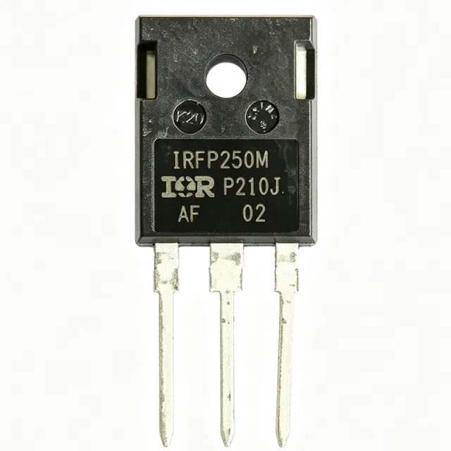
IRFP250MPBF - 200V 30A N-Channel HEXFET MOSFET | Infineon
The Infineon IRFP250MPBF is an N-channel 200V, 30A HEXFET power MOSFET housed in a TO-247AC (3-pin through-hole) package. It uses Infineon's advanced IR MOSFET process technology to deliver an extremely low on-resistance of 75 mΩ (max) per silicon area, combined with fast switching speed and rugged avalanche-rated device design. A power MOSFET (Metal-Oxide-Semiconductor Field-Effect Transistor) is a voltage-controlled semiconductor switch used to switch or amplify power in electronic circuits. Within the semiconductor taxonomy, MOSFETs sit under discrete semiconductors -> transistors -> MOSFETs; the N-channel enhancement-mode variant is the most common type used in switching power supply, motor drive, and inverter applications because it offers lower on-resistance per die area than equivalent P-channel parts. Key features include a 200V drain-to-source breakdown voltage (Vds), 30A continuous drain current (Id) at Tc=25°C, 75 mΩ maximum static on-resistance (RDS(on)) at Vgs=10V, and a power dissipation rating of 214W (Tc). The device is avalanche-rated and characterized for fast switching, making it well suited for hard-switched topologies. A typical gate threshold Vgs(th) of 4V and total gate charge of 82 nC (Qg) allow simple gate-drive compatibility with standard 10V MOSFET drivers. Internally, the IRFP250MPBF uses Infineon's proprietary HEXFET cell geometry with a vertical DMOS structure, achieving low RDS(on) while preserving a robust body diode for inductive-load switching. The TO-247AC package provides a low thermal resistance path through the metal tab, enabling the 214W power rating at case temperatures up to 25°C and supporting high-current pulsed operation above 100A for short durations. Typical applications include switch-mode power supplies (SMPS), DC-DC converters, motor drives, uninterruptible power supplies (UPS), solar inverters, and high-current switching circuits. The wide 200V rating also makes it suitable for offline PFC stages, full-bridge converters, and automotive 48V mild-hybrid systems where avalanche ruggedness is required. When designing with this part, verify that the switching frequency and gate-drive circuit stay within the safe operating area (SOA) at the worst-case load. Always use a gate resistor (typically 10-100 Ω) to control dv/dt and ringing, and ensure the heatsink is sized so the junction temperature stays below 175°C under maximum steady-state dissipation. This page synthesizes distributor pricing, drop-in alternatives, and practical design notes not found in the manufacturer datasheet.
IRFP250N - 200V 30A N-Channel HEXFET MOSFET | Infineon (Lead-Free (Pb-Free))
The Infineon IRFP250N is a fifth-generation N-Channel HEXFET power MOSFET rated at 200 V VDS, 30 A continuous drain current (at TC), and 214 W power dissipation (at TC), housed in a through-hole TO-247AC package. It leverages advanced process technology to achieve extremely low on-resistance per silicon area, paired with the fast switching speed and ruggedized device design HEXFET MOSFETs are renowned for. The PBF suffix confirms lead-free (Pb-free) construction compliant with RoHS directives. A power MOSFET is a voltage-controlled semiconductor switch that uses an electric field at the gate to modulate current flow between drain and source. Within the broader hierarchy, the IRFP250N sits as: power MOSFET -> discrete semiconductor -> N-channel enhancement-mode device -> HEXFET family (Infineon/IR proprietary planar cell technology). The planar cell structure gives a wide safe operating area (SOA), which is essential for inductive switching loads such as motors and transformers. Key features include dynamic dv/dt rating, ease of paralleling, fully avalanche-rated performance, simple drive requirements, and fast switching. The TO-247AC through-hole package provides low thermal resistance and is a long-standing industry-standard footprint, which simplifies PCB layout, mounting hardware selection, and heatsink attachment. The part is silicon-optimized for applications switching below 100 kHz and is qualified per JEDEC standards. The fifth-generation HEXFET process reduces conduction losses (low RDS(on)) while preserving the ruggedness that designers expect from earlier generations. Avalanche energy rating ensures the device can absorb unclamped inductive switching transients without destructive failure, an important attribute in motor drive and solenoid circuits where back-EMF is unavoidable. Typical applications include high-power DC-DC converters, uninterruptible power supplies (UPS), solar inverters, motor drive circuits (H-bridge and three-phase), welding equipment, induction heating, and switched-mode power supplies (SMPS) at the 1-5 kW power level. The 200 V rating also makes it suitable for 120 V rectified bus and PFC boost stages. When designing with this part, carefully calculate worst-case power dissipation (P = I^2 x RDS(on)) and verify that the chosen heatsink keeps Tj below 175 C. The gate drive voltage should swing between 10 V and 12 V for full enhancement and minimum RDS(on); under-driven gates dramatically increase conduction loss. This page synthesizes distributor pricing, drop-in alternatives in the TO-247AC footprint, and practical design notes not found in the manufacturer datasheet alone.
IRFP250NPBF - 200V 30A N-Channel HEXFET MOSFET | Infineon
The Infineon IRFP250NPBF is a fifth-generation N-Channel HEXFET power MOSFET rated at 200 V VDS, 30 A continuous drain current (at TC), and 214 W power dissipation (at TC), housed in a through-hole TO-247AC package. It leverages advanced process technology to achieve extremely low on-resistance per silicon area, paired with the fast switching speed and ruggedized device design HEXFET MOSFETs are renowned for. The PBF suffix confirms lead-free (Pb-free) construction compliant with RoHS directives. A power MOSFET is a voltage-controlled semiconductor switch that uses an electric field at the gate to modulate current flow between drain and source. Within the broader hierarchy, the IRFP250NPBF sits as: power MOSFET -> discrete semiconductor -> N-channel enhancement-mode device -> HEXFET family (Infineon/IR proprietary planar cell technology). The planar cell structure gives a wide safe operating area (SOA), which is essential for inductive switching loads such as motors and transformers. Key features include dynamic dv/dt rating, ease of paralleling, fully avalanche-rated performance, simple drive requirements, and fast switching. The TO-247AC through-hole package provides low thermal resistance and is a long-standing industry-standard footprint, which simplifies PCB layout, mounting hardware selection, and heatsink attachment. The part is silicon-optimized for applications switching below 100 kHz and is qualified per JEDEC standards. The fifth-generation HEXFET process reduces conduction losses (low RDS(on)) while preserving the ruggedness that designers expect from earlier generations. Avalanche energy rating ensures the device can absorb unclamped inductive switching transients without destructive failure, an important attribute in motor drive and solenoid circuits where back-EMF is unavoidable. Typical applications include high-power DC-DC converters, uninterruptible power supplies (UPS), solar inverters, motor drive circuits (H-bridge and three-phase), welding equipment, induction heating, and switched-mode power supplies (SMPS) at the 1-5 kW power level. The 200 V rating also makes it suitable for 120 V rectified bus and PFC boost stages. When designing with this part, carefully calculate worst-case power dissipation (P = I^2 x RDS(on)) and verify that the chosen heatsink keeps Tj below 175 C. The gate drive voltage should swing between 10 V and 12 V for full enhancement and minimum RDS(on); under-driven gates dramatically increase conduction loss. This page synthesizes distributor pricing, drop-in alternatives in the TO-247AC footprint, and practical design notes not found in the manufacturer datasheet alone.
IRFP260MPBF - 200V 50A N-Channel MOSFET | Infineon TO-247AC
The Infineon IRFP260MPBF is a 200V N-channel power MOSFET rated at 50A continuous drain current (Tc) and 300W power dissipation (Tc), housed in a TO-247AC through-hole package. It belongs to Infineon's HEXFET Power MOSFET family and uses IR MOSFET advanced process technology to achieve very low on-resistance per silicon area combined with fast switching speed and rugged avalanche-rated device design. A power MOSFET (Metal-Oxide-Semiconductor Field-Effect Transistor) is a voltage-controlled semiconductor switch used for high-current, high-voltage power conversion. N-channel MOSFETs such as the IRFP260MPBF conduct when the gate is pulled high relative to the source, and they form the active element in synchronous rectifiers, half-bridge and full-bridge converters, and motor drive stages. The TO-247AC package is a three-lead through-hole outline with an exposed metal tab that doubles as the drain terminal and as a mounting surface for heatsinking. Key specifications for the IRFP260MPBF include a maximum drain-source voltage (VDS) of 200V, continuous drain current of 50A at 25C case temperature, pulsed drain current capability that supports short-duration overloads, a typical on-resistance (RDS(on)) of 40 mOhm, and an input capacitance (Ciss) of approximately 1560 pF. The device is avalanche-rated, meaning it can dissipate the energy of an unclamped inductive load transient without destruction. Architecturally, the IRFP260MPBF uses a planar cell layout optimized for low conduction loss. The 200V breakdown rating, combined with the low RDS(on), places this part in the sweet spot for offline switch-mode power supplies below 1 kW, high-current DC motor drives, and welding inverter front ends. The rugged avalanche energy rating reflects Infineon's qualification methodology for industrial stress conditions. Typical applications include switch-mode power supplies (SMPS), uninterruptible power supplies (UPS), DC motor control, welding inverters, and DC choppers. The TO-247AC package allows single-screw isolated mounting for clean heatsink assembly. When designing with the IRFP260MPBF, ensure the gate driver can source and sink the gate charge required to switch the device within the desired transition time. A gate-source pull-down resistor of 10 kOhm is recommended to prevent accidental turn-on from Miller current during the drain transition. This page synthesizes distributor pricing, pin-compatible drop-in alternatives, and practical design notes that complement the manufacturer datasheet for fast engineering evaluation.