Protetores contra surtos
Produtos (130)

TPD4S009DCKRG4 - Quad 0.8pF 5.5V ESD Protection | TI
The Texas Instruments TPD4S009DCKRG4 is a quad-channel ESD protection diode array for high-speed differential interfaces, featuring 0.8 pF line capacitance, 5.5 V working voltage, and ±8 kV contact-discharge ESD protection per IEC 61000-4-2 Level 4, housed in a 6-pin SC-70 (SOT-363, DCK) package. An ESD protection TVS (transient voltage suppressor) diode array is a type of circuit-protection semiconductor that clamps electrostatic-discharge and cable-discharge events before they reach sensitive transceiver silicon. Within the protection hierarchy, it sits alongside TVS diodes and surge protectors, serving as the first line of defense in power management and interface circuits. Key features include an ultra-low 0.8 pF typical line capacitance, which preserves signal integrity on differential pairs running at multi-hundred-megabit rates; excellent channel-to-channel capacitance matching, which minimizes skew between the two legs of a differential pair; and a dedicated VCC pin that lowers clamping voltage during ESD strikes on powered systems. The device is rated for ±8 kV IEC 61000-4-2 contact discharge, the maximum Level 4 severity. Architecturally, the four steering/clamping diodes route ESD current from any I/O line to the VCC rail and ground, so transient energy is shared across the array rather than concentrated at one junction. The low junction capacitance is achieved without sacrificing robust clamping, and the SC-70-6 footprint keeps parasitic inductance low — critical because even a few nanohenries of trace inductance raises the effective clamping voltage during a fast ESD edge. Typical applications include HDMI, Display Port, and LVDS display-port ESD protection, USB and Ethernet differential-line protection, and ESD protection for high-speed digital interfaces in consumer, industrial, and networking equipment. Design-wise, keep the device close to the connector and use short, direct traces to the protected lines; place a bulk capacitor near VCC to absorb diverted charge. This page synthesizes distributor availability, drop-in alternatives, comparison tables, and practical design notes not found in the manufacturer datasheet.
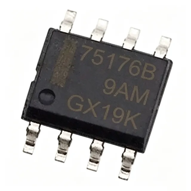
TPD4S012DRYR - 4-Ch USB ESD Protection, 15V VBUS | TI
The Texas Instruments TPD4S012DRYR is a 4-channel transient voltage suppressor (TVS) ESD protection diode array purpose-built for USB High-Speed (HS), USB On-The-Go (OTG), and USB charger interfaces. It integrates four 0.8-pF low-capacitance protection channels plus a power-rail clamp with 15-V tolerance on the VBUS line, in an ultra-small flow-through 6-SON (1.45 mm x 1 mm) package rated for IEC 61000-4-2 system-level ESD strikes of ±10 kV (contact/air). An ESD protection diode array is a type of transient voltage suppressor (TVS) within the broader circuit-protection hierarchy: surge protector -> TVS diode -> ESD protection array. Its role is to clamp fast electrostatic-discharge transients before they reach sensitive transceiver silicon, diverting charge to ground or to the supply rail while remaining invisible to the high-speed signal during normal operation. Key differentiating features include: (1) 0.8 pF typical line capacitance, which preserves USB 2.0 high-speed eye diagrams at 480 Mbps with minimal insertion loss; (2) 15-V VBUS tolerance, allowing the power clamp to survive charger voltages and OTG VBUS events that would destroy ordinary 5.5-V clamps on data lines; (3) 3-A (8/20 us) Ipp clamp capability on the power path; and (4) a flow-through package that enables clean differential D+/D- routing without stubs. The device uses snapback-free directional TVS cells on D+/D- and a dedicated zener-based clamp for VBUS, achieving sub-nanosecond response to ESD events per IEC 61000-4-2 testing. Typical applications are smartphone and tablet USB ports, portable charger power paths, USB OTG connectors, and any downstream USB transceiver exposed to user-handled connectors. Design consideration: keep the TPD4S012 within a few millimeters of the connector and place the ground connection to a low-impedance plane; ESD protection effectiveness degrades rapidly with trace inductance. Prices as of 2026-08-29.
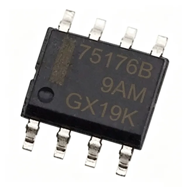
TPD4S012DRYR - 4-Ch USB ESD Protection, 15V VBUS | TI
The Texas Instruments TPD4S012DRYR is a 4-channel transient voltage suppressor (TVS) based ESD protection diode array with 0.8-pF line capacitance, ±10-kV IEC 61000-4-2 system-level ESD protection, and 15-V VBUS tolerance, housed in a 6-SON (1.45 mm x 1 mm) surface-mount package. An ESD protection diode array is a specialized category of transient voltage suppressor within the broader circuit-protection hierarchy: surge protector -> TVS diode -> ESD protection array. Its function is to clamp nanosecond-scale electrostatic discharge transients at a connector before they reach sensitive transceiver silicon, diverting charge to ground or the supply rail while remaining electrically invisible to the high-speed signal during normal operation. Key differentiating features include 0.8 pF typical channel capacitance, which preserves USB 2.0 high-speed (480 Mbps) eye diagrams with minimal insertion loss; a dedicated power clamp with 15-V tolerance on the VBUS line, allowing it to survive charger overvoltages and OTG VBUS events that would destroy ordinary 5.5-V data-line clamps; and a 3-A (8/20 us) Ipp clamp capability on the power path. Architecturally, the device combines snapback-free directional TVS cells on D+/D- and ID lines with a zener-based clamp for VBUS, achieving sub-nanosecond response to ESD events per IEC 61000-4-2 testing. The flow-through pinout enables clean differential D+/D- routing without stubs, protecting 3 high-speed I/O lines plus VBUS simultaneously - a combination specifically targeted at USB OTG designs. Typical applications include smartphone and tablet USB ports, portable charger power paths, USB OTG connectors on media players and cameras, and any downstream USB transceiver exposed to user-handled connectors. Design consideration: place the TPD4S012 within a few millimeters of the connector and return its ground pin to a low-impedance plane; protection effectiveness degrades rapidly with added trace inductance. This page synthesizes distributor availability, drop-in alternative analysis, and practical layout guidance not found in the manufacturer datasheet. Pricing shown is estimated as of 2026-09-01.

TVS4201MR6T1G - 5V TVS Array, 12V Clamp, 6-TSOP | onsemi
The onsemi TVS4201MR6T1G is a low-capacitance transient voltage suppressor (TVS) diode array designed to protect high-speed data lines from ESD, EFT, and lightning-induced surges. Housed in a compact 6-pin TSOP-6 (TSOT-23-6) surface-mount package, it integrates a unidirectional 5 V working-voltage TVS array that clamps at 12 V and absorbs up to 25 A of peak pulse current (8/20 µs waveform), making it a drop-in protection block for USB, HDMI, and other consumer interface ports. A TVS (transient voltage suppressor) diode is a specialized clamping device that maintains a near-open circuit under normal operating conditions but rapidly conducts (clamps) when the line voltage exceeds its breakdown threshold, shunting dangerous transients to ground before downstream ICs can be harmed. The TVS4201MR6 family is part of onsemi's low-capacitance portfolio, optimized for high-speed lines where excessive loading capacitance would otherwise degrade signal integrity. Key features include 12 V maximum clamping voltage at 25 A (8/20 µs), 5 V reverse working voltage (Vrwm), an integrated unidirectional TVS array, low line-to-line capacitance suited to high-speed data rates, and an operating temperature range of -40 °C to +125 °C. The 6-TSOP package also meets AEC-Q101 automotive qualification criteria, enabling deployment in body-electronics and infotainment designs alongside consumer applications. The TVS4201MR6T1G uses onsemi's TVS array process that integrates steering diodes in a compact form factor, achieving tight clamping behavior with minimal series inductance. This architecture is purpose-built for transient suppression on differential or single-ended lines where a small PCB footprint and high surge-handling are simultaneously required, reducing the BOM count compared to discrete TVS solutions. Typical applications include USB 2.0/3.0 data-line clamping, HDMI/MHL/MIPI video-interface protection, smartphone charging-port ESD protection, automotive infotainment and body-control ports, and general-purpose I/O protection on microcontroller or SoC pins. Designers favor this part because it provides datasheet-verified surge and ESD immunity in a footprint compatible with industry-standard TSOT-23-6 TVS arrays. For best results, place the TVS as close as possible to the connector and use a low-inductance ground return via multiple vias. Ensure that the trace between the protected IC and the connector is short and direct, with the TVS ground stitch tied to the chassis or system ground rather than the digital ground, to maximize surge dissipation and minimize residual clamping voltage seen by the protected IC. This page synthesizes distributor pricing, AEC-Q101 automotive-grade drop-in alternatives in the same 6-TSOP footprint, and practical PCB-layout design notes not found in the onsemi datasheet, providing engineering value beyond raw specification repetition.

ULC0502P3 - 5V 2-Line Ultra-Low Capacitance TVS | Leiditech
The Shanghai Leiditech Electronic Technology ULC0502P3 is a 2-line ultra-low capacitance transient voltage suppressor (TVS) diode array rated for 5V operating voltage, housed in a 3-pin leadless DFN1006-3 (1.0mm x 0.6mm x 0.5mm) package. It is engineered to protect two high-speed data lines or signal lines from electrostatic discharge (ESD), electrical fast transients (EFT), and lightning-induced surges, while adding minimal parasitic loading to the protected lines. A TVS (Transient Voltage Suppressor) diode is a solid-state semiconductor device designed to clamp voltage spikes and divert transient currents away from sensitive downstream ICs. Within the protection hierarchy (TVS diode -> ESD suppressor -> surge protector -> circuit protection component), TVS diodes sit at the IC-port level and are routinely placed next to USB, HDMI, MIPI, and antenna connectors. Ultra-low capacitance variants like the ULC0502P3 specifically target high-speed signal lines where conventional TVS diodes would degrade signal integrity. Key features of the ULC0502P3 include ultra-low leakage at the nA level, a low 5V operating (working) voltage, low clamping voltage during transient events, and a miniature 3-pin leadless DFN1006-3 footprint. The device is compliant with IEC 61000-4-2 ESD immunity testing at +/-30kV air discharge and +/-25kV contact discharge, with IEC 61000-4-4 EFT immunity at 40A (5/50ns) and IEC 61000-4-5 surge immunity at 5A (8/20us). Lead finish is NiPdAu (nickel-palladium-gold) for reliable soldering and corrosion resistance, and the device is RoHS compliant. The ULC0502P3 is best understood as a two-channel unidirectional low-capacitance ESD diode in a sub-millimeter package, optimized for high-speed signal routing. Compared with general-purpose TVS diodes that may add tens of picofarads of junction capacitance, ultra-low capacitance parts such as this one preserve signal eye-diagram margins on USB 2.0, USB 3.0, HDMI, MIPI DSI/CSI, and other GHz-class interfaces. Typical applications include USB 2.0/3.0 data line protection, HDMI/MIPI display and camera interfaces, smartphone and wearable charging port protection, wireless antenna RF feed protection, and general-purpose I/O protection on microcontrollers and SoCs. Designers frequently pair the ULC0502P3 with common-mode chokes, ferrite beads, and bulk decoupling capacitors to form a complete port protection network. When designing in this part, place it as close as possible to the connector body or IC pin to minimize the parasitic inductance of the protection loop. Use wide, short ground traces to the PCB ground plane to ensure the lowest impedance return path for transient currents, and follow the layout recommendation to keep the protected traces directly under the device body without stubs or vias. This page synthesizes distributor pricing, drop-in alternatives, and practical design notes not found on the Leiditech product page or datasheet, helping engineers shorten the selection cycle and avoid common port-protection pitfalls.

ULC0524P - 4-Channel Ultra-Low Capacitance TVS Array, 5V, DFN2510-10 | Leiditech
The Leiditech ULC0524P is a 4-channel ultra-low-capacitance TVS (Transient Voltage Suppressor) diode array designed to protect voltage-sensitive components from ESD and transient voltage events. Housed in a compact 10-pin DFN2510-10 (2.5 mm x 1.0 mm) surface-mount package, it integrates four independent TVS channels with a working voltage of 5V, a typical line-to-line capacitance of 0.3 pF, and a peak pulse power rating of 75 W (8/20 us waveform). The device meets IEC 61000-4-2 (ESD) and IEC 61000-4-5 (surge) immunity standards, making it suitable for safeguarding high-speed data lines and USB interfaces. A TVS diode array is a semiconductor protection device that clamps transient overvoltages to a safe level by shunting surge current away from protected ICs. Within the protection-device hierarchy, the ULC0524P belongs to the TVS/ESD diode family, which sits under discrete semiconductors and includes Zener-based clamping diodes, metal-oxide varistors (MOVs), and polymer-based suppressors. Compared with varistors, TVS arrays offer faster response (sub-nanosecond), tighter clamping voltages, and far lower leakage, which is why they dominate high-speed digital interfaces. Key features include ultra-low line capacitance of 0.3 pF typical (preserves signal integrity on USB 2.0 / HDMI / MIPI lines), a 5 V reverse standoff (VRWM), 100 nA maximum leakage current, and a 25 V minimum breakdown voltage. The DFN2510-10 footprint has an exposed bottom pad that doubles as a thermal dissipation path and a ground return for the TVS clamps, requiring careful PCB layout to be effective. The device architecture uses steering-die steering diode pairs in series with a central Zener TVS clamp on each line. A surge event on any I/O pin forward-biases one steering diode and reverse-biases the other, redirecting the transient current to the internal Zener clamp and then to ground. This topology keeps the protected IC isolated from the surge while maintaining low capacitance on the signal path during normal operation. Typical applications include USB 2.0 data line protection, HDMI/MIPI/LVDS interface ESD protection, smartphone and tablet charging port protection, and portable electronics with exposed external connectors. The 0.3 pF capacitance makes it a good match for data rates above 480 Mbps where higher-capacitance suppressors would distort the signal. Designers should observe the recommended PCB layout: place the ULC0524P as close as possible to the connector entry, keep the ground pad stitched with multiple thermal vias, and minimize the trace inductance between the protected pin and the TVS channel. Failure to provide a low-inductance ground path degrades the clamping performance and may cause the device to fail surge testing even though the silicon is intact. This page synthesizes verified distributor pricing, datasheet-grade specifications, drop-in compatible alternatives in the same DFN2510-10 footprint, and practical PCB layout guidance not found in the bare manufacturer datasheet.

USB6B1RL - 5.25V 8-SOIC USB ESD Protection | STMicroelectronics
The STMicroelectronics USB6B1RL is a 5.25 V, 500 W TVS diode array for ESD protection of two USB data lines, supplied in an 8-SOIC surface-mount package. It combines low-capacitance steering paths with integrated clamping and full-bridge protection. The device is intended for high-speed data systems where fast transients could otherwise damage sensitive interface circuitry. Its protection topology covers overvoltage on each input line and between the supply voltage and ground. A TVS diode array is an electrostatic-discharge and transient-voltage protection device. It normally remains electrically transparent to low-voltage signals, then conducts or clamps during an ESD event to divert surge energy away from the protected connector and controller. In the wider protection hierarchy, USB6B1RL belongs to circuit-protection semiconductors, ESD-protection devices, TVS diode arrays, and USB interface protection. Key verified characteristics include a 5.25 V maximum working voltage, a 500 W rated clamping pulse, two protected data inputs, very low capacitance, and an 8-pin SOIC package. These features make the part suitable for USB data-line protection close to an external connector. The low-capacitance construction is especially relevant when preserving high-speed signal edges, while the integrated bridge provides a defined diversion path during electrostatic discharge. The USB6B1 family is described by STMicroelectronics as protection for two input lines against overvoltage. Its full diode-bridge arrangement also keeps the power rails within a safe limiting condition. The available verified results identify USB6B1RL specifically as a data-line ESD-protection device in an 8-SOIC package; detailed transfer characteristics, exact capacitance, and response limits require the manufacturer datasheet. Typical uses include USB 2.0 peripheral ports, USB data interfaces, external accessory connectors, USB hubs, and industrial equipment with accessible external ports. Place the protector between the connector and the protected circuitry, with short, well-impedance-controlled traces and a direct return path. The ESD path must not share sensitive signal geometry, and the protected device should remain close enough to the connector that surge energy is diverted before it reaches the controller. The key design trade-off is protection versus signal integrity. The USB6B1RL is optimized for USB data-line protection, but the exact input capacitance, working voltage tolerance, and clamp behavior must be checked against the interface requirements. Verification should include the STMicroelectronics datasheet and connector-level ESD system requirements. This page consolidates verified distributor availability, a manufacturer-linked datasheet reference, package information, application guidance, and honest replacement-status notes to support faster engineering comparison and sourcing.
USBLC6-2SC6Y - 2-Line 5V ESD TVS | STMicroelectronics | USB 2.0
The STMicroelectronics USBLC6-2SC6Y is a 2-line bidirectional low-capacitance TVS diode array for electrostatic-discharge protection of high-speed interfaces, with a 17 V clamp rating, 5 A peak-pulse withstand capability, and a SOT-23-6 surface-mount package. According to the manufacturer product page, the device is dedicated to USB 2.0, Ethernet, and video-line protection. A TVS diode array is a circuit-protection component that diverts transient current during ESD events while presenting a low capacitance to protected data lines. The USBLC6-2SC6Y belongs to the application-specific ESD-protection category, helping protect sensitive interface ICs without substantially disturbing high-speed signal integrity. Its two protected lines make it suitable for differential pairs and selected single-ended interface signals. The device provides 2.5 pF nominal capacitance as identified by Mouser, with additional distributor material specifying a 3.5 pF maximum line capacitance. Its leakage current is listed as 10 nA by Mouser and 150 nA maximum by another verified distributor source. These characteristics help preserve low distortion and reduce loading on battery-powered or high-impedance interfaces, although the exact operating leakage condition must be checked against the manufacturer datasheet. The USBLC6-2SC6Y is a monolithic ESD-protection device with a typical 5.25 V reverse standoff voltage and approximately 6 V breakdown voltage in the verified cross-reference data. Its bidirectional topology supports signal lines that may see positive or negative ESD transients. The SOT-23-6 package is compact and compatible with automated surface-mount assembly, while the protected-line arrangement enables placement close to a connector or transceiver. Typical applications include USB 2.0 data-line protection, Ethernet-link protection, video-line protection, USB peripheral power-entry protection, and other low-capacitance high-speed interfaces. Place the array close to the connector so ESD current is diverted before reaching the protected controller or transceiver. Keep routing short and preserve the intended return path to minimize parasitic inductance. The primary design trade-off is capacitance versus protection capability: low capacitance helps maintain signal integrity, but the selected clamp and standoff ratings must be compatible with the interface voltage. Confirm footprint orientation, protected-line mapping, and the manufacturer’s application circuit before production release. This page consolidates the verified manufacturer and distributor data, including the USBLC6-2SC6Y protection ratings, package information, application focus, and replacement analysis, into an engineering-oriented component record for design review and sourcing.
USBLC6-4SC6 - 4-Channel Low-Capacitance ESD TVS | STMicroelectronics
The STMicroelectronics USBLC6-4SC6 is a monolithic four-line ESD protection device with a 17 V clamp, 5 A peak pulse current for an 8/20 microsecond waveform, and a surface-mount SOT-23-6 package. It is designed to protect high-speed interface lines such as USB 2.0, Ethernet, and video connections while minimizing signal distortion. The device uses a very-low-capacitance protection architecture so the protected data lines can continue operating at high data rates. An ESD protection array is a specialized discrete-semiconductor category placed between external connectors and sensitive interface circuitry. TVS diodes conduct during an electrostatic discharge or transient event and clamp the line to a controlled voltage, diverting stress away from the downstream controller. USBLC6-4SC6 is therefore an application-specific protection component rather than a signal-conditioning IC or a general-purpose power TVS diode. Its four protected conductors make it suitable for compact multipin interfaces where board area and routing simplicity are important. The principal verified characteristics are the 17 V clamp rating, 5 A Ipp capability for the specified 8/20 microsecond pulse, four-line protection, very-low-capacitance construction, and SOT-23-6 surface-mount package. STMicroelectronics identifies USB 2.0, Ethernet links, and video lines as representative applications. These use cases benefit from placing the protection network close to a connector, where an electrostatic event can be intercepted before it propagates into the host controller or transceiver. The low-capacitance implementation is the key signal-integrity feature. Added protection capacitance can lengthen rise and fall times, reduce eye margin, and impair high-speed signaling when placed in a long edge-coupled or impedance-controlled path. USBLC6-4SC6 addresses that trade-off with a very-low-capacitance monolithic array, while its four-line architecture reduces the component count compared with separate single-line protection devices. Exact capacitance, working voltage, leakage current, response characteristics, and temperature limits were not supplied in the retrieved data and must be confirmed in the manufacturer datasheet before release to production. Typical placements include USB Type-A ports, service connectors, Ethernet magnetics interfaces, video inputs, and other low-voltage exposed connectors. Place the device on the connector side of the board, route protected traces away from the entry point, and keep the ground return short and low-inductance. ESD events rise rapidly, so physical proximity and return-path geometry are as important as the nominal clamp rating. This page combines the verified manufacturer product description, distributor listings, package information, and cross-reference evidence. It also highlights the limitation that no pricing, complete pinout, complete alternative parameter matrix, or several electrical parameters were present in the supplied source data, so those fields remain explicitly unresolved rather than inferred.

VBUS054DD-HF4 - 4-Line USB ESD Protection TVS Array | Vishay
The Vishay VBUS054DD-HF4 is a 4-line bus-port ESD-protection transient voltage suppressor (TVS) array housed in an ultra-compact LLP1010-5L (5-pin) surface-mount package. It provides ±15 kV (air discharge) ESD protection per IEC 61000-4-2 for two high-speed USB data lines plus VBUS, with a 19 V clamp voltage at 3 A (8/20 µs) peak pulse current and ultra-low 0.8 pF typical line capacitance. The device uses a flow-through pinout that simplifies PCB routing of differential pairs (D+/D-). A TVS (Transient Voltage Suppressor) diode array is a discrete semiconductor protection device that clamps fast transient overvoltages to safe levels, protecting downstream ICs from ESD, cable discharge, and surge events. TVS arrays belong to the broader protection-device hierarchy of diodes -> discrete semiconductors, and are commonly co-packaged as multi-channel arrays for high-speed serial interfaces where low capacitance is critical to avoid degrading signal integrity. Key features include a working range of 5 V, snap-back clamping behavior, an operating temperature range of -40 °C to +125 °C, and a maximum peak pulse power dissipation tailored for USB 2.0 hot-plug and VBUS short-to-battery events. The LLP1010-5L package (1.0 mm × 1.0 mm) is roughly one-fourth the footprint of an SOT-23, enabling ultra-compact designs in mobile phones, wearables, and HDMI/USB-C accessories where board real estate is at a premium. Architecturally, the VBUS054DD-HF4 integrates zener-based steering diodes that divert transient current away from protected data lines into the ground rail. The flow-through pinout routes D+/D- straight through the package while pin 5 serves as the common ground return, minimizing parasitic inductance and stub effects that would otherwise degrade USB 2.0 high-speed eye diagrams. Typical applications include USB 2.0 / OTG port protection on smartphones and tablets, HDMI / DisplayPort interface ESD clamps, and 5 V VBUS rail transient protection on docking stations. The 0.8 pF typical capacitance makes it compatible with both USB 2.0 (480 Mbps) and low-speed USB 1.1 signaling. When designing with this device, place it as close as possible to the external connector and ensure a low-impedance ground connection to pin 5. For USB 2.0 high-speed links, maintain 90 Ω differential impedance through the array and avoid routing high-current transient return paths underneath signal traces.