Устройства защиты от импульсных перенапряжений
Товары (67)

0402ESDA-05N - 5V Bidirectional Polymer ESD Suppressor | BORN
The BORN 0402ESDA-05N is a bidirectional polymer ESD suppressor with a 5V working voltage, 50V clamp-side breakdown capability, ultra-low 1.5 pF line capacitance, and 1 nA leakage current, housed in a 2-terminal 0402 (1005 metric) surface-mount package. It is qualified to suppress electrostatic discharge events per IEC 61000-4-2 and operates over a -40C to +85C industrial temperature range. A polymer ESD suppressor is a type of transient voltage suppression device within the broader family of TVS diodes and circuit protection components. Unlike silicon avalanche TVS diodes, polymer suppressors use a conductive polymer material that switches from a high-impedance state to a low-impedance state within nanoseconds when an ESD transient exceeds its trigger threshold, shunting the surge energy away from the protected IC. This technology enables extremely low parasitic capacitance, which is the defining parameter for high-speed data line protection. Key features of the 0402ESDA-05N include its 1.5 pF typical capacitance, which minimizes signal insertion loss on USB 2.0, HDMI, and other multi-gigabit interfaces; its bidirectional 5V standoff rating suited to both single-ended and symmetric data lines; and its nanosecond response time to IEC 61000-4-2 contact and air discharges. The 1 nA reverse leakage keeps standby power consumption negligible in battery-powered designs. The polymer construction provides no DC clamping action under normal operating conditions, so the line sees essentially the suppressor capacitance only. During an ESD event, the device transitions to a conductive state and recovers automatically after the transient passes, requiring no replacement or reset. The compact 0402 footprint allows placement directly adjacent to the connector pins. Typical applications include high-speed data port protection on smartphones, tablets, and set-top boxes; ESD protection for USB, HDMI, and antenna lines in consumer electronics; and protection of sensitive RF front-ends where capacitance must stay below 2 pF. Design tip: place the suppressor as close to the connector as possible with minimal stub length, following the zero-stub pad guidance common to polymer ESD devices, so the transient is clamped before it propagates down the trace. This page synthesizes distributor pricing, drop-in alternatives, and practical design notes not found in the manufacturer datasheet.

1.5KE11CA - 1500W Bidirectional TVS, 9.4V VRWM | Littelfuse
The Littelfuse 1.5KE11CA is a 1500W bidirectional axial-leaded Transient Voltage Suppressor (TVS) diode designed to clamp voltage transients induced by lightning, inductive load switching, and ESD events on sensitive electronic equipment. According to the Littelfuse datasheet, it features a Reverse Working Standoff Voltage (VRWM) of 9.4V, a Breakdown Voltage range of 10.5V to 11.6V, a maximum clamping voltage of 15.6V at 97.4A peak pulse current, and is housed in a DO-201 through-hole axial package. A TVS diode is a solid-state avalanche device engineered to shunt large transient currents away from downstream circuitry in microseconds, providing far faster response than MOVs or PTC fuses. TVS diodes sit at the bottom of the protection hierarchy as discrete semiconductors, fall under the surge-protector family, and serve as the first-line defense on DC power rails, signal lines, and automotive bus networks where predictable clamping behavior is mandatory. Key differentiating specifications include 1500W peak pulse power dissipation at a 10/1000 microsecond waveform, a peak pulse current (IPPM) of 97.4A, glass-passivated chip junction construction for long-term reliability, low Zener impedance, and a maximum clamping voltage of 15.6V that keeps downstream 12V logic rails well within their absolute-maximum ratings during surge events. The bidirectional (CA suffix) variant conducts transients of either polarity, eliminating orientation errors during PCB assembly. Architecturally, the 1.5KE11CA is a silicon PN-junction avalanche suppressor with a glass-passivated surface that suppresses leakage and stabilizes breakdown characteristics across the -55C to +175C operating range. The avalanche breakdown mechanism provides sub-microsecond response, ensuring that fast-rise transients such as those defined by IEC 61000-4-2 are clamped before sensitive ICs see the overvoltage. Typical applications include 12V automotive load-dump protection per ISO 7637-2, industrial PLC 24V rail transient suppression, telecom -48V battery backplane protection, USB and HDMI port ESD/lightning protection on consumer devices, and protection of SMPS auxiliary windings from flyback spikes. The wide standoff-voltage range and 1500W rating also suit PoE PSE input protection. When designing with this part, derate surge power for temperatures above 75C using the derating curve in the datasheet, ensure lead bend radius exceeds 1.5mm to avoid axial-package cracking, and place the TVS within 50mm of the protected connector for maximum effectiveness. For multi-stage protection, pair the 1.5KE11CA with an upstream GDT or PTC to coordinate energy dissipation. This page synthesizes current distributor pricing, drop-in cross-brand equivalents, parametric comparison tables, and practical design notes not found in the manufacturer datasheet alone - giving the engineer a one-stop reference for sourcing and qualifying the 1.5KE11CA in new or existing designs.
1.5KE11CA-B - 1500W Bi-Directional TVS Diode 9.4V | Littelfuse
The Littelfuse 1.5KE11CA-B is a 1500 W axial-leaded bidirectional Transient Voltage Suppressor (TVS) diode rated at 9.4 V working standoff voltage (VRWM), 10.5 V minimum breakdown voltage, and 15.6 V maximum clamping voltage at 97.4 A peak pulse current, housed in a DO-201 (DO-27) through-hole axial package. It is designed to clamp fast transient overvoltages such as those induced by lightning, inductive load switching, and ESD, protecting downstream sensitive electronics. A TVS diode (Transient Voltage Suppressor) is a semiconductor protection device belonging to the surge protector / discrete semiconductor family. Under normal operation it presents a high-impedance path; when a transient exceeds its breakdown voltage, it avalanches into a low-impedance state within picoseconds, shunting surge energy away from protected circuits. TVS diodes sit hierarchically under discrete semiconductors -> diodes -> surge protectors, and are commonly used alongside MOVs, gas discharge tubes, and PTC resettable fuses in multi-stage protection networks. The bidirectional ('CA') construction means a single device clamps both positive and negative transients, making it ideal for AC lines and differential signal interfaces. Key specifications include 1500 W peak pulse power (10/1000 µs waveform), 97.4 A peak pulse current (IPP), <1 ps typical response time, low clamping factor (15.6 V VC / 9.4 V VRWM = 1.66), and an operating temperature range that supports industrial environments. The 5 % voltage tolerance ('A' suffix) and bidirectional polarity ('C') make the 1.5KE11CA-B particularly suited for protecting 12 V system rails, RS-485 interfaces, and telecom line cards where induced surges from outdoor cabling are common. The 1.5KE11CA-B uses a silicon PN-junction avalanche structure manufactured in a glass-passivated die, packaged in a transfer-molded DO-201 body with tin-plated axial leads for wave or hand soldering. Its robust construction supports IEC 61000-4-2 (ESD) and IEC 61000-4-5 (surge) immunity testing when properly designed into the protection network. Typical applications include 12 V automotive load-dump suppression, telecommunications line-card secondary protection, industrial 24 V PLC and sensor protection, and consumer electronics AC/DC adapter input protection. Designers should place the TVS as close to the connector or transient entry point as possible, with short, wide PCB traces to minimize parasitic inductance. Design tip: combine the 1.5KE11CA-B with a PTC resettable fuse or series resistor upstream to limit sustained fault current and extend device lifetime under repeated surge events. This page synthesizes distributor pricing, drop-in equivalents from multiple brands, and practical protection-design guidance not consolidated on any single manufacturer page.
1.5KE16ARL4G - 1500W 16V Unidirectional TVS | onsemi
The onsemi 1.5KE16ARL4G is a 1500 W axial-leaded unidirectional Transient Voltage Suppressor (TVS) diode in the Surmetic DO-201AA package, designed to clamp high-energy transients and protect voltage-sensitive downstream components. The part delivers a working standoff of 13.6 V, a minimum breakdown of 15.2 V, and a maximum clamping voltage of 22.5 V at the rated 67 A peak pulse current (Ipp) per the 10/1000 µs waveform. A Transient Voltage Suppressor (TVS) is a specialized clamping diode that operates in avalanche breakdown when the line experiences a fast over-voltage event such as an ESD pulse, inductive load kickback, or lightning-induced surge. TVS diodes sit at the front of the protection topology, upstream of bulk protection (fuses, PTCs) and downstream of the exposed connector; their job is to divert surge current away from sensitive ICs within microseconds. The 1.5KE family is the workhorse 1500 W industrial/automotive grade series defined by JEDEC register DO-201AA axial outlines. Key features of the 1.5KE16ARL4G include 1500 W peak pulse power (10/1000 µs waveform), 67 A peak pulse current (Ipp), unidirectional polarity, a typical clamping voltage of 22.5 V at Ipp, low Zener impedance in breakdown, fast response time (sub-nanosecond), and a maximum clamping factor that ensures the protected downstream rail stays within its absolute-maximum rating. The Surmetic axial package is a through-hole DO-201AA body with robust leads suitable for wave-soldering and high-vibration environments. Technically, the 1.5KE16ARL4G uses a large-junction silicon die designed for non-repetitive high-energy avalanche. Peak pulse power is specified for a 10/1000 µs exponential waveform per the industry-standard TVS test method; steady-state power dissipation is rated at 5 W (with appropriate lead length derating). Reverse leakage at standoff is in the µA range, allowing the part to remain in-circuit without measurable quiescent loss. Typical applications include DC power-line protection on 12 V industrial bus rails, automotive 12 V load-dump protection, secondary protection behind a primary TVS or PTC on long signal lines, protection of telecom line drivers, and suppression of inductive kickback from relays, solenoids, and motor windings. It is also widely used in switch-mode power supply (SMPS) output rectification and snubbing. When designing with this part, derate peak pulse power for shorter pulses (the 8/20 µs waveform allows higher Ipp) and ensure lead length matches the datasheet's thermal derating curve. Avoid continuous operation in breakdown - this part is intended for transient clamping only, not as a voltage regulator.
1.5KE18AG - 18V 1500W Unidirectional TVS | onsemi
The onsemi 1.5KE18AG is a 1500 W unidirectional Mosorb Zener Transient Voltage Suppressor (TVS) in an axial-leaded through-hole package, designed to protect voltage-sensitive components from high-voltage, high-energy transients. The "1.5KE" series defines a family of glass-passivated-junction transient voltage suppressors widely used as circuit-protection devices. A TVS diode is a solid-state silicon device that clamps an overvoltage event by avalanche breakdown, shunting transient energy away from downstream circuitry. Within the broader protection hierarchy, TVS diodes sit alongside metal-oxide varistors (MOVs) and gas discharge tubes as fast-response (< 1 ns) suppressors, prized over fuses because they self-recover after the transient has decayed. Key features of the 1.5KE18AG include a working standoff voltage of 15.3 V, a maximum clamping voltage of 25.2 V at 59.5 A peak pulse current, and a peak pulse power rating of 1500 W for an 8/20 us waveform (per IEC 61000-4-5). The device offers unidirectional polarity, a glass-passivated die for stability, and a Surmetic axial package with operating junction temperature up to 175 C. The 1.5KE18AG uses an avalanche-mode silicon-junction Zener die, where the junction is glass-passivated for long-term stability and moisture resistance. Its low Zener impedance and fast response time allow it to clamp transient events from ESD, inductive load kickback, and lightning-induced surges within nanoseconds. Typical applications include protection of 12 V and 15 V dc power rails, automotive ECU inputs, industrial PLC I/O lines, telecom -48 V system protection, and USB/HDMI interface guarding on consumer equipment. When selecting layout, mount the 1.5KE18AG as close as possible to the protected connector or IC pin and minimize lead length to reduce parasitic inductance, which otherwise degrades clamping effectiveness at high dv/dt. This page synthesizes distributor pricing, drop-in alternatives, and practical design notes not found in the manufacturer datasheet, giving engineers a single anchor for board-level protection decisions.

1.5SMC8.2A-E3/9AT - 1500W 8.2V Uni-Dir TVS | Vishay
The Vishay 1.5SMC8.2A-E3/9AT is a 1500W peak-pulse-power unidirectional TRANSZORB transient voltage suppressor (TVS) diode rated at a 8.2V working standoff voltage, packaged in the industry-standard DO-214AB (SMCJ) surface-mount outline. It is engineered to clamp 12.1V at a peak pulse current of 124A (10/1000 µs waveform) and protect downstream electronics from induced lightning, load-dump, and ESD transients on DC rails. A TVS diode (Transient Voltage Suppressor) is a clamping semiconductor that operates in avalanche breakdown when the voltage across it exceeds a defined threshold. It belongs to the protective-component hierarchy: TVS diode → ESD/surge protector → discrete semiconductor → circuit protection device. Under normal operation the part presents a high-impedance path; when a transient pushes the line above its breakdown voltage (8.2V nominal / 7.02V reverse standoff), it conducts in nanoseconds and shunts the surge energy to ground, holding the protected rail to a safe clamping voltage. Key specifications include a 1500W peak pulse power dissipation on a 10/1000 µs waveform, 124A peak pulse current (Ipp), 12.1V maximum clamping voltage at Ipp, and a glass-passivated chip junction that improves long-term reliability under repetitive surge events. The TRANSZORB series uses a low-profile DO-214AB package suitable for automated placement and offers uni-directional (suffix A) polarity. Architecturally, the device is a silicon avalanche junction that has been glass-passivivated for environmental stability and given a low-inductance, large-area die bond to handle the 1500W transient. The flip-chip-style construction minimizes lead inductance so the clamping response remains sub-nanosecond, preserving the protected IC's input stage during fast-edge ESD events. Typical applications include 12V automotive load-dump protection, industrial 24V bus transient suppression, USB Type-C VBUS line protection, and telecom port protection against secondary lightning surges. Any low-voltage DC rail driving sensitive CMOS logic, microcontrollers, or RF transceivers in harsh EMI environments can leverage this part. When designing with this device, observe the derating curve over temperature - peak pulse power falls linearly from 1500W at 25°C toward zero at the maximum TJ. Place the TVS as close as possible to the connector entry point and keep the trace to ground short and wide to minimize parasitic inductance that would otherwise let voltage overshoot above the 12.1V clamp rating. This page synthesizes distributor pricing, parametric drop-in alternatives sourced from cross-reference tools, and applied design guidance beyond what is published in the manufacturer's datasheet alone.
1.5SMCJ54C - 1500W TVS Diode 54V Bidirectional SMC | Diotec
The Diotec 1.5SMCJ54C is a 1500 W peak-pulse surface-mount transient voltage suppressor (TVS) diode in a bidirectional configuration with a stand-off working voltage of 54 V, housed in a DO-214AB (SMC) plastic package. It is engineered to clamp fast transient events such as ESD, EFT, and lightning-induced surges on 48 V telecom, industrial-bus, and DC power-distribution lines, providing a maximum clamping voltage of approximately 87.1 V at the rated 1500 W peak pulse power (10/1000 µs waveform). What is a TVS diode? A transient voltage suppressor is a discrete semiconductor protection device that responds to over-voltage events in the nanosecond time domain by avalanching into a low-impedance state, shunting surge current away from sensitive downstream circuitry. TVS diodes sit within the broader hierarchy of discrete semiconductors (diodes -> protection devices -> TVS) and are commonly specified alongside metal-oxide varistors (MOVs) and gas discharge tubes (GDTs) as a second-tier clamp after primary over-current protection. The "C" suffix indicates bidirectional operation, meaning a single part protects both polarities of an AC or DC-coupled bus without orientation sensitivity. Key features include a minimum breakdown voltage of 60.0 V and a maximum breakdown of 66.0 V at 1 mA, a maximum reverse leakage of 5 µA at the rated stand-off, a peak forward surge rating suited for the SMC footprint, and a glass-passivated junction rated for 150 °C junction temperature. The low-profile DO-214AB (SMC) body has Underwriters Laboratory Flammability Classification 94V-0 and supports 260 °C / 10 s high-temperature soldering for lead-free reflow compatibility. Typical applications include 48 V PoE protection, telecom line-card secondary protection, industrial 24/48 V DC bus transient suppression, photovoltaic inverter input clamping, and DC motor drive H-bridge protection. Designers also use 1.5SMCJ54C series parts as secondary protection after a primary GDT or PTC to limit let-through energy. When designing with this device, verify that the chosen working voltage (Vrwm = 54 V) sits above the maximum continuous operating voltage of the protected bus, and confirm that the peak-pulse power derating curve at the expected surge duration does not exceed 1500 W. Bidirectional parts require no orientation marking, simplifying PCB layout and rework.

AQ15-02HTG - 15V 500W 2-Channel TVS Diode Array | Littelfuse
The Littelfuse AQ15-02HTG is a 2-channel, 500 W transient voltage suppressor (TVS) diode array designed to protect sensitive electronics from electrostatic discharge (ESD), electrical fast transients (EFT), and lightning-induced surges. Housed in a compact SOT-23-3 surface-mount package, it provides a working voltage of 15 V, a clamping voltage of 30 V at 15 A (8/20 µs), and a peak pulse power rating of 500 W (8/20 µs). A TVS diode array is a class of discrete semiconductor protection device that uses avalanche-breakdown junctions to clamp transient overvoltages to safe levels in microseconds. TVS arrays sit in the protection-component hierarchy between simple Zener clamps and multi-stage gas-discharge or polymer suppressors, and they belong to the broader category of circuit-protection semiconductors. By integrating two steering diodes and a central TVS die in a single 3-pin package, the AQxx-02HTG series provides differential or single-ended protection on data lines and power rails without requiring multiple discrete components. Key features include ±30 kV ESD protection per IEC 61000-4-2 (contact and air discharge), ultra-low capacitance of 85 pF suitable for high-speed interfaces, low clamping voltage of 30 V at 15 A peak pulse current, and a low leakage current of 1 µA at the working voltage. The SOT-23-3 package is footprint-compatible with industry-standard 3-pin SOT-23 outlines, enabling drop-in placement on existing PCB layouts. The AQ15-02HTG uses an avalanche-junction TVS structure combined with low-capacitance steering diodes, achieving sub-nanosecond turn-on time. This architecture absorbs repetitive strikes without performance degradation, making it ideal for industrial and automotive environments exposed to frequent ESD events. The 85 pF line capacitance is acceptable for CAN, RS-485, and general-purpose I/O protection but should be evaluated for USB 2.0 high-speed data lines where lower capacitance is preferred. Typical applications include industrial CAN bus protection, RS-485 transceiver protection, automotive ECU I/O protection, sensor interface protection, factory automation I/O, and consumer electronics ESD protection on USB and HDMI ports. The AQxx-02HTG series is AEC-Q101 qualified for automotive use. When designing with this device, place the AQ15-02HTG as close as possible to the connector or ESD entry point, keep the trace between the protected IC and the TVS short, and provide a low-impedance ground return to the chassis or earth ground. Avoid routing protected traces beneath the device to minimize parasitic coupling. This page synthesizes distributor pricing, drop-in alternatives, and practical layout guidance not aggregated in the manufacturer datasheet, giving engineers a single reference for component selection, BOM risk mitigation, and PCB design.

CDDFN2-T3V3SC - 3.3V Bidirectional TVS Diode, DFN-2 | Bourns
The Bourns CDDFN2-T3V3SC is a 3.3 V bidirectional surface-mount Transient Voltage Suppressor (TVS) housed in a sub-miniature DFN-2 (0402-size, 1.0 mm x 0.6 mm x 0.5 mm) package. It delivers ESD, EFT and surge protection for external ports of portable electronic devices and provides a typical clamping voltage of 9 V at 42 A peak pulse current (8/20 us waveform). The device is designed for direct PCB mounting on high-density I/O lines where a board area is impossible. A TVS diode is a semiconductor clamp that diverts over-voltage energy away from sensitive downstream circuitry. When the line voltage exceeds the device's breakdown threshold, the TVS enters avalanche breakdown within nanoseconds and shunts the transient current to ground, limiting the peak voltage seen by the protected IC. TVS diodes sit at the first tier of a protection scheme (next to gas-discharge tubes and PTC fuses) and are the fastest-responding element, making them ideal for suppressing ESD (electrostatic discharge) and EFT (electrical fast transient) events at connector pins. As a discrete protection component, the TVS diode belongs to the broader family of surge protection devices used in transient voltage suppression. Key specifications include a 3.3 V working voltage (VRWM), 9 V typical clamping voltage (VC) at 42 A Ipp (8/20 us), bidirectional polarity, and a sub-nanosecond response time. The DFN-2 (0402-style) package occupies 0.6 mm footprint area per side and operates across -55 C to +150 C. It is qualified to IEC 61000-4-2 (ESD) air-discharge ratings typical of the family, and the device is RoHS compliant and lead-free. The CDDFN2-T3V3SC uses a silicon avalanche junction in a bidirectional configuration, meaning a single device protects both polarities of an AC or differential data line. The 8/20 us surge waveform rating indicates the device can survive indirect lightning-induced surges and inductive load switching transients without degradation. Typical applications include USB 2.0/3.0 data line protection, HDMI/MIPI/MDDI interfaces, SIM card protection, headset/microphone audio jacks, portable set buttons, and any 3.3 V logic rail exposed to user contact. The DFN-2 footprint makes it especially suitable for compact handheld and wearable designs where every millimeter of PCB space counts. When designing with the CDDFN2-T3V3SC, ensure the protected signal line does not exceed the 3.3 V working voltage in normal operation, place the device as close as physically possible to the connector pin, and provide a low-impedance ground return directly beneath the package thermal pad. The device's low capacitance makes it compatible with high-speed data lines, but always verify the total channel capacitance against the interface specification.
CDDFN2-T5V0SC - 5V Bidirectional TVS Diode, 9.5V Clamp | Bourns
The Bourns CDDFN2-T5V0SC is a bidirectional surface-mount Transient Voltage Suppressor (TVS) diode rated at 5 V working voltage with a 9.5 V clamping voltage at 18 A peak pulse current (8/20 µs waveform), housed in a miniature 2-pin DFN (1.0 × 0.6 mm) package. It is engineered to absorb ESD, EFT, and surge transients on external I/O ports of portable and handheld electronics, and integrates a steering diode network for clean bidirectional clamping from either polarity. A Transient Voltage Suppressor (TVS) diode is a clamping semiconductor device designed to limit transient overvoltages by avalanching into a low-impedance state when its breakdown voltage is exceeded. Within the power management hierarchy, TVS diodes sit alongside ESD protection arrays and varistors as the first line of defense for sensitive downstream ICs, providing sub-nanosecond response and a defined non-linear V-I curve. Bidirectional TVS parts such as the CDDFN2-T5V0SC are particularly suited to AC-coupled signal lines and differential data buses where polarity can reverse. The CDDFN2-T5V0SC delivers 18 A peak pulse handling on the 8/20 µs surge waveform and is rated to absorb ESD strikes per IEC 61000-4-2 at both contact and air discharge levels. Its ultra-small 1.0 × 0.6 mm DFN footprint allows placement immediately at the connector, minimizing parasitic loop area and improving coupling efficiency into the suppressor. Low clamping factor and low dynamic resistance keep the residual voltage seen by downstream ICs well below their absolute-maximum ratings. Internally the device uses a Zener-based avalanche junction combined with a steering-diode bridge, giving symmetric positive and negative clamping. The low leakage at 5 V bias preserves battery life in always-connected portable designs, while the wide operating temperature range supports industrial and outdoor deployments. The leadless DFN-2 package offers a low-inductance current path that outperforms leaded alternatives such as SOD-123 at multi-kilovolt ESD. Typical applications include USB Type-C data line protection on smartphones, tablets, and laptops, HDMI/MIPI/LVDS interface protection on display panels, antenna port ESD protection on cellular and Wi-Fi modules, headset audio jack protection, and portable medical handheld devices. The wide surge rating also covers industrial sensor interfaces and IoT edge nodes that may be exposed to EFT or lightning-induced surges on long cable harnesses. Place the CDDFN2-T5V0SC as close as physically possible to the external connector pin, with a short, direct ground return to the chassis or board ground pour. Keep the trace between the protected line and the device under 2 mm to maximize ESD suppression, and avoid routing any sensitive analog signal traces underneath the pad to prevent coupling of residual transients. This page synthesizes distributor pricing tiers, verified drop-in alternatives, and PCB-layout guidance that go beyond what is shown on the Bourns datasheet, giving engineers a single source for selection, sourcing, and design-in.
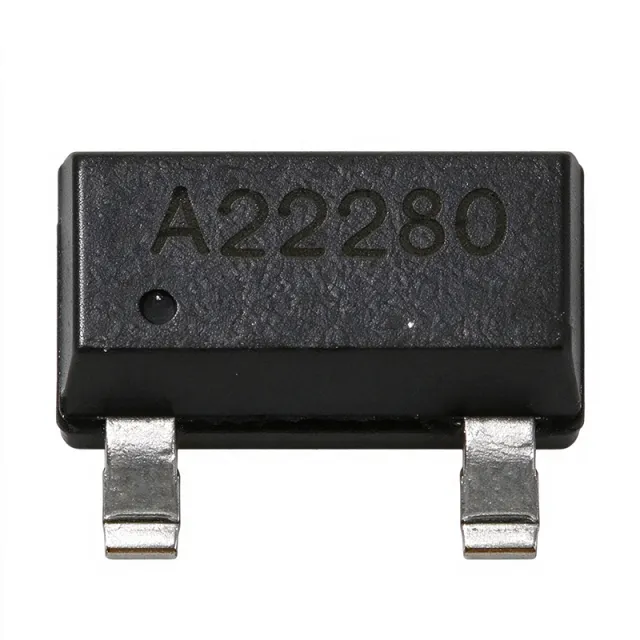
CDSOT23-SM712 - 7V/12V Asym RS-485 TVS Array 400W | Bourns
The Bourns CDSOT23-SM712 is a surface-mount transient voltage suppressor (TVS) diode array housed in a SOT-23-3 package, providing 400 W peak pulse power per line for asymmetrical protection of RS-485/RS-422 data lines. The device integrates two TVS diodes with a Working Peak Reverse Voltage of 7 V (positive side) and 12 V (negative side), Minimum Breakdown Voltage of 7.5 V and 13.3 V respectively, and maximum clamping voltages of 14 V and 26 V at 17 A (8/20 us waveform). The asymmetry is intentional - it tracks the wider negative common-mode range of RS-485 transceivers that must tolerate -7 V to +12 V. A TVS diode array is a specialized class of transient voltage suppressor that integrates multiple steering/clamps in one package to protect differential data ports. The CDSOT23-SM712 belongs to the diode array > TVS array > ESD protection IC > circuit protection hierarchy. These arrays are essential companions to bus transceivers (RS-485, CAN, Profibus), where the transceiver's own absolute-maximum ratings are routinely violated by ESD, EFT, or surge events on the bus cable. Key features include IEC 61000-4-2 (ESD) protection to +/-30 kV air and +/-30 kV contact, IEC 61000-4-4 (EFT) to 40 A (5/50 ns), and IEC 61000-4-5 (surge) to 17 A (8/20 us). The device provides low capacitance (per datasheet typical application) to preserve signal integrity at high data rates, and the SOT-23-3 footprint is the industry-standard pinout for SM712-style arrays. A low leakage current at 5 V maximises battery life in quiescent-mode industrial nodes. The CDSOT23-SM712 uses an asymmetric avalanche-breakdown architecture: the 7 V TVS clamps positive transients on each data line relative to ground, while the 12 V TVS clamps the larger negative excursions permitted by RS-485. This dual-window topology is more efficient than two identical TVS diodes, because a single 12 V symmetric array would clip legitimate -7 V bus signalling, while a 7 V symmetric array would not survive the -25 V cable discharge that the RS-485 standard tolerates. The Bourns design matches the SM712 reference footprint exactly, so engineers can swap between vendors (Bourns, ST, NXP, MSKSEMI, YINT) without PCB rework. Typical applications include RS-485/RS-422 fieldbus nodes in industrial automation, Profibus and Modbus links, CAN bus nodes in heavy machinery and EV charging, HVAC controllers, building automation, smart-meter communication ports, and any line-driver exposed to ESD during cable mating or lightning-induced surge on long outdoor runs. The asymmetrical window is also useful for CAN-H and CAN-L protection where one rail must withstand -12 V cross-wiring faults. When designing with this device, place the CDSOT23-SM712 within 10 mm of the bus connector and keep the ground return path short and wide. Do not rely on the TVS alone for surge survival above 17 A - upstream PTCs or PTC+fuse combinations may be required to meet IEC 61000-4-5 level 4. The SOT-23-3 pad pattern is identical to industry-standard SOT-23, allowing use of standard land pattern footprints. This page synthesizes distributor pricing, drop-in alternatives, and practical PCB layout notes not found in the manufacturer datasheet alone - including a same-package alternative table engineers can use when second-sourcing for supply-chain resilience.
ESD5481MUT3G - 5V Bidirectional ESD Protection TVS | onsemi | X3-DFN-2
The onsemi ESD5481MUT3G is a bidirectional ESD protection Zener/TVS diode housed in an ultra-compact 2-pin X3-DFN package measuring 0.6 x 0.3 mm (0201-equivalent footprint). It is engineered to protect voltage-sensitive components on data lines from electrostatic discharge (ESD) events, with a working voltage of 5 V, a clamping voltage of 15 V at 2 A (8/20 us waveform), and exceptionally low leakage current. A TVS (Transient Voltage Suppressor) diode is a specialized semiconductor device designed to clamp fast transient overvoltages - such as those caused by ESD strikes, cable discharge events, or inductive switching - to a safe level before they damage downstream ICs. In the broader hierarchy, TVS diodes belong to circuit protection devices, which sit alongside suppressors, fuses, and varistors under the umbrella of power management and protection semiconductors. Bidirectional TVS devices like the ESD5481MUT3G protect both positive and negative transients on AC or DC-coupled signal lines, simplifying PCB layout by eliminating orientation concerns. Key features of the ESD5481MUT3G include a 5 V reverse working voltage (VRWM), 15 V clamping voltage (VC) at the rated 2 A pulse, sub-nanosecond response time typical of TVS avalanche technology, and an extremely small PCB footprint suited to portable electronics. According to the onsemi datasheet, the device is designed to deliver best-in-class ESD clamping with low leakage and fast response. The architecture is a silicon avalanche-breakdown Zener structure, which inherently clamps at its breakdown voltage and resets automatically once the transient subsides - no manual reset or replacement is required. This makes it ideal for dense, miniaturized designs where serviceability is limited. Typical applications include USB 2.0/3.0 data line protection on smartphones, tablets, and wearables; HDMI/MIPI/LVDS interface protection; MP3 players, digital cameras, and other portable consumer electronics; and general-purpose I/O protection on microcontrollers and SoCs where board space is at a premium. When designing with the ESD5481MUT3G, place the device as close as possible to the connector or vulnerable pin, keep the ground return path short and wide, and pair it with proper chassis-ground bonding to maximize ESD dissipation. Always verify clamping voltage against the absolute maximum rating of the downstream IC. This page synthesizes distributor pricing, drop-in alternatives in the same X3-DFN package, and practical design guidance beyond what is found in the onsemi datasheet.
ESD762DBZR - ±24V Bidirectional ESD/TVS Diode | Texas Instruments
The Texas Instruments ESD762DBZR is a bidirectional dual-channel ESD protection diode rated at ±24 V working voltage with ±20 kV IEC 61000-4-2 air-gap ESD discharge tolerance and 1.7 pF typical line capacitance, housed in a 3-pin SOT-23 (DBZ) package. The device integrates a TVS (transient voltage suppressor) clamp structure that activates within nanoseconds, suppressing electrostatic discharge and surge transients that could otherwise damage downstream USB-PD controllers, audio codecs, or sensitive analog front ends. The '36 V (Typ)' clamping figure listed by distributors corresponds to the peak pulse voltage reached during an 8/20 µs surge event at 2.5 A peak pulse current. A TVS diode is a semiconductor clamp designed to protect interface lines (USB, HDMI, audio, GPIO, industrial buses) by diverting transient over-voltage energy away from protected ICs. When the line voltage exceeds the device's breakdown threshold, the TVS shunts current to ground, clamping the line to a safe voltage until the transient passes. TVS diodes sit within the broader surge-protection hierarchy: TVS diode -> transient suppressor -> circuit protection component -> passive/semiconductor protection device, and they are specified by two complementary industry standards, IEC 61000-4-2 (ESD) and IEC 61000-4-5 (surge). Key features include 1.7 pF typical diode capacitance (suitable for USB 2.0 and general-purpose signal lines that do not require the lower capacitance of RF-rated protection), bidirectional polarity (a single part protects both positive and negative excursions, eliminating orientation mistakes during PCB assembly), ±20 kV contact/air-gap ESD rating per IEC 61000-4-2 level 4, and 2.5 A peak pulse current handling on the 8/20 µs waveform. The SOT-23-3 footprint offers a compact 2.9 mm x 1.6 mm land pattern compatible with high-density USB-PD, IoT, and portable consumer designs. The ESD762 uses a Zener-triggered avalanche clamp architecture. Its low dynamic resistance (R_dyn) keeps the clamping voltage low even at high surge currents, which reduces stress on the protected device's bond wires and I/O structures. Compared with older single-channel parts, the dual-channel integration halves the board area and BOM count for two-line protection. Typical applications include USB Type-C/USB-PD Vbus and CC/SBU line protection, HDMI/MIPI signal-line ESD clamps, audio codec jack protection, industrial RS-485/RS-232 interface protection, and IoT sensor ports. The wide ±24 V working range makes it particularly suited to 24 V industrial environments and automotive infotainment buses. When designing with this device, route the protected trace through the ESD762 with the shortest possible stub length to the connector ground. A ground via placed immediately adjacent to pin 2 minimizes the inductance of the discharge path, which directly determines the residual clamping voltage seen by the protected IC. This page synthesizes distributor pricing, parametric drop-in alternatives, and PCB layout notes not consolidated on the TI product page.
ESD9B3.3ST5G - Bidirectional ESD TVS Diode 3.3V SOD-923 | onsemi
The onsemi ESD9B3.3ST5G is a bidirectional transient voltage suppressor (TVS) diode for ESD protection with a 3.3 V reverse working voltage, 11.5 V clamping voltage, and 2 A (8/20 us) peak pulse current capability, housed in a 2-pin SOD-923 surface-mount package. A TVS diode is a type of clamp circuit protection device in the broader family of transient voltage suppressors and surge protection components. Placed in parallel with a sensitive signal or power line, it remains high-impedance during normal operation and conducts within nanoseconds when an ESD or surge transient exceeds its breakdown voltage, diverting the surge energy to ground and clamping the line voltage to a safe level. The ESD9B Series is designed to protect voltage-sensitive components from ESD. According to the onsemi ESD9B datasheet, the series offers excellent clamping capability, low leakage, and fast response time for best-in-class protection on designs exposed to ESD events. The bidirectional 3.3 V configuration supports symmetric positive and negative transient clamping on lines operating up to 3.3 V rails, with IEC 61000-4-2 style ESD robustness of plus or minus 18 kV (air and contact) as reported by distributor listings. Architecturally, the device uses a silicon avalanche breakdown structure that requires no external drive, no control logic, and no supply rail, making it a zero-quiescent-current protection element. Its micro-packaged SOD-923 footprint minimizes loop inductance, which directly improves clamping performance on fast-rise-time ESD waveforms; shorter loop inductance equals lower residual clamped voltage at the protected IC. Typical applications include cellular phones, MP3 players, digital cameras, tablets, and other portable electronics where board space comes at a premium. The ESD9B3.3ST5G is commonly placed on USB data lines, button/keypad inputs, audio jack lines, GPIO pins, and antenna-fed RF lines running from 3.3 V or lower rails. Design consideration: place the TVS as close as possible to the connector or entry point and route to a low-impedance ground stitch; the series inductance of a long trace will dominate the residual clamp voltage during a nanosecond ESD pulse. This page synthesizes verified distributor data, pricing tiers, drop-in alternatives, and practical ESD layout design notes not found in the manufacturer datasheet, providing selection guidance for engineers choosing between 3.3 V and 5 V bidirectional micro-packaged TVS options.
ESD9X5.0ST5G - 5V ESD TVS Diode SOD-923 | onsemi
The onsemi ESD9X5.0ST5G is a uni-directional ESD protection TVS diode with a 5V reverse working voltage, 12.3V typical clamping voltage at 8.7A (8/20us waveform) peak pulse current, housed in an ultra-small 2-pin SOD-923 surface-mount package. A TVS (Transient Voltage Suppressors) diode is a clamping device that reacts to electrostatic discharge and other fast transient overvoltage events within nanoseconds, diverting damaging current away from sensitive ICs. Within the semiconductor hierarchy, the ESD9X5.0ST5G belongs to the ESD protection diode family, a subset of the TVS diode category, which itself sits under discrete protection semiconductors in circuit-protection systems. Key features include excellent clamping capability, low leakage current, and fast response time, which onsemi describes as providing best-in-class protection for designs exposed to ESD threats. The device withstands ESD strikes up to +/-30kV per distributor listings and handles 8.7A of peak pulse current on the industry-standard 8/20us waveform. Its 5V reverse standoff voltage makes it suitable for protecting 5V and lower logic rails without significant loading. The ESD9X Series architecture uses a silicon avalanche clamping structure that activates within nanoseconds of a transient event. Unlike crowbar-type protection devices, it clamps without latching, returning to a high-impedance state automatically after the surge passes. Low junction capacitance keeps signal integrity intact on moderately fast digital lines. Typical applications include cellular phones, MP3 players, digital cameras, and other portable electronics where board space is at a premium. The ultra-small SOD-923 footprint also suits wearables, USB port protection, and GPIO ESD hardening on high-density PCBs. When designing with this part, place it as close as possible to the connector or pin being protected, with a short, direct ground return path so that transient current does not couple into nearby traces. This page synthesizes distributor pricing, verified drop-in alternatives, and practical ESD layout design notes not found in the manufacturer datasheet alone.

ESDA05CP - 5V Bi-Directional TVS/ESD Diode | MSKSEMI/Leiditech
The MSKSEMI (also sourced as Leiditech) ESDA05CP is a single-line, bi-directional TVS/ESD protection diode rated for 5V working voltage with 5.6V typical breakdown, housed in an ultra-compact DFN1006-2L (1.0 mm x 0.6 mm) surface-mount package. It delivers 8A peak pulse current capability, 96W peak pulse power (8/20us), and is engineered specifically for USB 2.0 power and data line protection. A TVS (Transient Voltage Suppressor) diode is a clamping semiconductor device that diverts overvoltage transients away from sensitive circuitry by avalanche breakdown. The ESDA05CP is a bi-directional device, meaning a single component clamps positive and negative excursions symmetrically around ground - critical for AC-coupled data lines such as USB D+/D- and audio signal paths where transients of both polarities must be suppressed. The 5V working voltage matches common logic rails (USB VBUS, 3.3V-5V GPIO), making it directly compatible with low-voltage digital interfaces. Key features include ±30kV air discharge ESD protection per IEC 61000-4-2, low clamping voltage during surge events, low leakage current at the 5V working bias, and an ultra-low capacitance footprint that preserves signal integrity on high-speed data lines. The DFN1006-2L package occupies less than 0.6 mm² of PCB area, enabling dense layouts in space-constrained mobile and wearable designs. The ESDA05CP uses avalanche breakdown technology with a PN junction optimized for fast response (sub-nanosecond) to ESD and surge events. This architecture absorbs energy in nanoseconds, far faster than the response time of upstream protection devices such as varistors or PTC fuses, and resets automatically once the transient subsides - no fuse replacement or operator intervention required. Typical applications include USB 2.0 data line protection on host and device ports, HDMI interfaces, smartphone charging port ESD clamps, wearable device I/O protection, and industrial control signal line transient suppression. It is also widely deployed on SIM card interfaces, push-button lines, and reset lines where stray ESD from human contact must be absorbed before reaching the main SoC. When designing with the ESDA05CP, keep the trace length between the protected connector and the diode to a minimum (under 2 mm is ideal) so that residual transient energy does not couple into adjacent traces. Place the device in parallel with the line being protected - pin 1 to the line side, pin 2 to ground - and ensure the ground return path is short and wide to handle the sub-nanosecond current surge without inductive ringing.

ESDALC6V1-5BTG - 5-Line ESD Protection TVS, 6.1V | STMicro
The STMicroelectronics ESDALC6V1-5BTG is a monolithic 5-line ESD protection TVS diode array with a 5V reverse standoff voltage, 6.1V minimum breakdown voltage, and 14V maximum clamping voltage at 2.5A (8/20 us), housed in a 6-pin SOT-23-6 surface-mount package. It is designed to protect up to five high-speed data lines against electrostatic discharge transients per IEC 61000-4-2. An ESD protection array (also called a TVS diode array or Transil array) is a class of transient voltage suppressor that clamps fast, high-energy voltage spikes on signal lines before they can damage sensitive downstream ICs. Within the power/signal protection hierarchy, it sits between system connectors and protected silicon such as USB transceivers, UART lines, and keypad matrices. Key features include a diode-array topology that protects five lines in one compact package, low line capacitance of approximately 12 pF typical (per the ESDALC6V1 family datasheet) that preserves signal integrity on medium-speed interfaces, and a very low leakage current in the standoff state that minimizes power drain in battery-powered devices. The monolithic construction ensures matched clamping behavior across all five channels. Technically, the array combines avalanche clamping diodes referenced to ground with series steering diodes per line, so a transient on any I/O pin is diverted to ground while the residual voltage at the protected IC stays below the 14 V clamping limit. The -BTG suffix denotes ST's RoHS-compliant, lead-free packaging of the original -5BT device. Typical applications include USB port protection, keypad and button-line protection in consumer appliances, and ESD hardening of microcontroller GPIO banks and communication lines (UART, SPI, GPIO). Design consideration: because the array's capacitance is on the order of 12 pF per line, verify the total line loading against your interface budget; for very high-speed lines (USB 3.x, MIPI), select a lower-capacitance ESD part instead. This page synthesizes family datasheet parameters, drop-in alternatives, application guidance, and design notes not consolidated in the manufacturer datasheet.

LM1K24CA - 30kW Bi-Directional TVS Diode, 24V SMB | Leiditech
The Leiditech LM1K24CA is a high-power bi-directional transient voltage suppressor (TVS) diode rated at 30 kW peak pulse power (8/20 us waveform) with a 24 V reverse stand-off voltage, housed in the SMB (DO-214AA) surface-mount package. It is engineered to clamp fast transients such as induced lightning surges, ESD strikes, and inductive load switching, protecting downstream ICs, field-effect devices, and signal interfaces in industrial and automotive environments. A TVS (transient voltage suppressor) diode is a clamping semiconductor device that operates in avalanche breakdown when the applied voltage exceeds its breakdown threshold, diverting transient energy away from sensitive circuitry. Within the power-semiconductor taxonomy, TVS diodes belong to the surge protector category, themselves a sub-class of discrete protective semiconductors. Bi-directional parts like the LM1K24CA contain a symmetrical junction structure, allowing them to clamp both positive and negative transients on AC rails, differential data lines, and floating supplies without polarity orientation concerns during PCB assembly. Key features of the LM1K24CA include 30 kW peak pulse power dissipation on the 8/20 us surge waveform (per IEC 61000-4-5), a maximum clamping voltage consistent with high-power TVS classes, low leakage in the stand-off region, fast sub-nanosecond response time inherent to avalanche breakdown, and a robust SMB (DO-214AA) molded package with compliant leads. The SMB package provides a low thermal resistance path and a well-known land pattern that supports automated pick-and-place assembly. Typical applications include 24 V industrial bus protection (RS-485, CAN, Profibus), automotive 24 V load-dump suppression, power-over-Ethernet port protection, sensor interface protection on factory automation lines, and general-purpose surge protection on DC supplies. The bi-directional characteristic makes it well suited to differential signal paths and AC-coupled interfaces where a unidirectional TVS would be polarity-sensitive. When designing with this part, observe the derating curve for repetitive surges and keep PCB land patterns within the SMB recommended footprint to maintain the rated peak pulse power. Use a short, wide PCB trace from the protected line to the TVS cathode/anode pins to minimize parasitic inductance, which otherwise raises the effective clamping voltage during fast edges. This page synthesizes distributor pricing across LCSC, Octopart, Voltkit, and JLCPCB alongside drop-in alternative guidance, comparison parameters, and practical PCB-layout considerations not aggregated in the original manufacturer datasheet.
LXES02TAA1-144 - 5pF 5.5V ESD TVS Diode 2-WLCSP | Murata
The Murata Electronics LXES02TAA1-144 is a single-channel silicon ESD (electrostatic discharge) protection TVS diode packaged in an ultra-compact 2-pin WLCSP (Wafer-Level Chip-Scale Package) measuring 0.40 mm x 0.20 mm. It features a 5.0 pF typical line-to-ground capacitance, a 7.0 V minimum breakdown voltage (VBR), a 5.5 V reverse stand-off voltage, and is rated to withstand 8 kV contact discharge per the IEC 61000-4-2 standard. According to the manufacturer datasheet, the part is qualified to consumer-equipment ESD stress profiles. An ESD protection diode (also known as a TVS diode or transient voltage suppressor) is a passive semiconductor device placed in parallel with a sensitive signal line or rail to clamp fast electrostatic discharge transients and prevent damage to downstream ICs. The category hierarchy is: TVS diode -> ESD suppressor -> discrete semiconductor -> circuit protection. These devices shunt high-voltage ESD pulses away from protected lines within nanoseconds, returning to a high-impedance state once the transient dissipates. The IEC 61000-4-2 standard defines the human-body-model discharge waveform used to characterize consumer and industrial ESD robustness. Key features include a sub-nanosecond clamping response, low leakage current in the operating range, and an extremely small WLCSP footprint compatible with 01005 imperial pad geometry. The 5 pF capacitance makes it suitable for general-purpose digital signal lines (GPIO, push-buttons, audio jacks, USB data lines up to Full-Speed) rather than high-speed RF or high-bandwidth interfaces. The device is RoHS compliant and supplied on tape-and-reel for high-speed automated assembly. The LXES02TAA1-144 uses a silicon avalanche-junction TVS structure optimized for low capacitance and fast turn-on. At 5.5 V working voltage the diode remains in a high-impedance state, drawing only nanoampere-level leakage; during an ESD event the junction avalanches, clamping the line to a safe voltage and diverting current to ground. The 7 V minimum VBR provides adequate margin for 3.3 V and 5 V rails. Typical applications include ESD protection for consumer handheld devices, smartphone accessory lines, wearables, audio codec jack pins, GPIO buttons, low-speed data interfaces, and battery-management contact pins. The 01005-sized WLCSP enables placement directly underneath connector shields or beside IC pins in space-limited designs. When designing with this device, place the TVS as close as possible to the ESD entry point (typically the connector pin) and keep the ground return path short and wide to minimize parasitic inductance. Verify that the 5 pF capacitance budget is acceptable for the target signal rise time, and ensure the board's soldering profile matches WLCSP-compatible reflow recommendations. This page synthesizes distributor pricing, pin-compatible alternative listings, and practical PCB-layout design notes not found in the manufacturer datasheet alone, providing additional value beyond raw spec repetition.

LXES02TAA1-145 - 5.5V 0.35pF WLCSP ESD TVS Diode | Murata
The Murata LXES02TAA1-145 is a single-channel ESD protection TVS diode housed in an ultra-compact 2-pin WLCSP (0.40 x 0.20 mm) package, also referenced as CSP0402. Per the Murata official product page, the device provides a reverse stand-off voltage of 5.5V, a breakdown voltage (VBR) of 7V, an ultra-low capacitance of 0.35 pF, and IEC 61000-4-2 contact discharge ratings of 8 kV, making it well-suited for protecting high-speed signal lines on space-constrained consumer PCBs. What is a TVS diode? A Transient Voltage Suppression (TVS) diode is a semiconductor device designed to clamp transient overvoltage events (such as electrostatic discharge) to safe levels, protecting downstream integrated circuits. Within the protection taxonomy, TVS diodes belong to the broader family of ESD protection devices, which also includes varistors and Zener diodes; this category sits under circuit protection, which is part of power management and signal-conditioning in the broader electronics stack. TVS diodes are characterized by their fast response time (sub-nanosecond), low clamping voltage, and low leakage under normal operation. Key features include an extremely low capacitance of 0.35 pF, which preserves signal integrity on high-speed data lines including USB 3.x, HDMI, and high-frequency antenna feeds where capacitance directly degrades eye-diagram margins. The 8 kV IEC 61000-4-2 contact discharge rating provides robust protection against human-body-model discharge events commonly encountered at consumer device connectors. The 5.5V working voltage covers standard 3.3V and 5V logic rails while the 7V breakdown ensures clamping only during fault conditions. The WLCSP-2 package measures only 0.40 x 0.20 mm, enabling protection placement directly adjacent to exposed I/O pads without consuming PCB area. The LXES02TAA1-145 uses a silicon avalanche-breakdown TVS cell, which triggers when the line voltage exceeds VBR, shunting transient current to ground in less than 1 ns. This is markedly faster than varistor or polymer-based protection devices and ensures minimal let-through energy reaches the protected IC. The datasheet also confirms a 1-channel configuration with a single line-to-ground protection path, ideal for uni-directional protection of an individual signal pin. Typical applications include USB 3.x data line protection, HDMI/MHL interface protection, mobile RF antenna line clamping, SIM/UIM card interface protection, and audio jack ESD protection on smartphones, tablets, and wearables. Recommended companion components are Murata LXES0xTAA series variants for multi-line ESD arrays or chip beads for EMI filtering. Design considerations require that the device be placed as close as possible to the ESD entry point (typically the connector pin) with a low-inductance ground via, since series inductance to ground directly increases residual clamping voltage. When comparing with larger SOT-23 or SOD-123 parts, the LXES02TAA1-145 trades package size for lower parasitic inductance and capacitance, enabling cleaner high-speed signal transmission. This page synthesizes distributor pricing, drop-in alternatives, and practical design notes not found in the manufacturer datasheet alone, providing engineers with a consolidated reference for the LXES02TAA1-145.

LXES03TAA1-199 - 1pF Bi-Dir ESD Diode 0201 | Murata | USB/HDMI
The Murata LXES03TAA1-199 is a single-channel, ultra-low capacitance bi-directional ESD protection diode housed in an industry-standard 0201 (0.6 x 0.3 mm) surface-mount package. Designed for high-speed signal interfaces, it integrates a TVS (transient voltage suppressor) clamp capable of handling 1.5 A peak pulse current (8/20 µs waveform) while presenting only 1.0 pF typical line capacitance, preserving signal integrity on data lines up to multi-Gbps speeds. The device clamps transients at a minimum breakdown voltage of 7.0 V (VBR) and offers a reverse stand-off (working) voltage of 5.5 V, making it compatible with 3.3 V and 5 V logic rails commonly used in consumer and industrial systems. A TVS diode is a specialized solid-state clamping device that diverts ESD and surge energy away from sensitive downstream ICs. In the protection hierarchy, TVS diodes sit at the connector-facing edge of a system, ahead of any series ferrite or common-mode choke and ahead of the PHY/MCU. The LXES family is specifically engineered for ultra-low parasitic capacitance to avoid attenuating or distorting high-frequency signals such as USB 2.0/3.x, HDMI, MIPI DSI/CSI-2, and antenna RF feeds. Bi-directional polarity allows placement across a differential pair or single-ended line without regard to DC bias direction. Key features include a 30 kV contact-discharge rating per IEC 61000-4-2, an ultra-compact 0201 footprint (0.6 x 0.3 x 0.3 mm), and RoHS-compliant lead-free reflow profile compatibility. The package integrates two back-to-back steering diodes plus a TVS cell in a single die, minimizing loop inductance and maximizing clamping response time relative to discrete alternatives. Architecturally, the LXES03TAA1-199 uses silicon avalanche technology, where the TVS junction breaks down at a controlled voltage (VBR) and shunts current to ground. The 1.0 pF typical capacitance is achieved through die geometry optimization and minimizes insertion-loss impact above 1 GHz. Source: Murata product data referenced on the official Murata EMEA product page (pim.murata.com / murata.com LXES T Series listing). Typical applications include USB 2.0/3.0 high-speed data line protection, HDMI/MHL interface ESD clamps, smartphone antenna and SIM interfaces, wearable device charging ports, and IoT sensor data lines. Its miniature 0201 size makes it suitable for boards where PCB real estate is at a premium, such as mobile phones, TWS earbuds, AR/VR headsets, and compact sensor modules. When designing in the LXES03TAA1-199, place it as close as possible to the connector with a short, wide ground return to the chassis or system ground. Avoid routing protected signal traces under the diode; the ungrounded paddle and pad geometry already provide adequate isolation but a clean ground via is essential. The 0201 size requires precise SMT stencil aperture control for reliable solder joint formation during reflow. This page synthesizes Murata datasheet specifications, distributor pricing, and cross-reference drop-in alternatives for engineers evaluating the LXES03TAA1-199 in space-constrained, high-frequency interface designs.
LXES03TBB1-141 - 0.05pF ESD/TVS Diode 2-CSP | Murata
The Murata LXES03TBB1-141 is a single-channel ultra-low-capacitance bidirectional silicon ESD protection diode housed in a miniature 2-CSP (0.60 x 0.30 mm) surface-mount package. It offers 0.45 pF typical capacitance, a 5.5 V reverse stand-off voltage, and a minimum breakdown voltage (VBR) of 7.0 V. Peak pulse power (8/20 us) is rated at 125 W, making it suitable for absorbing fast transient discharges on high-speed signal lines. A TVS (transient voltage suppressor) diode is a semiconductor clamp designed to protect sensitive downstream electronics by diverting voltage transients - electrostatic discharge (ESD), cable discharge events, and surge pulses - away from the protected IC. It belongs to the broader category of surge protectors, which also includes varistors (MOVs), gas discharge tubes, and TVS diode arrays. In modern compact PCB designs, silicon TVS diodes are preferred over MOVs because they offer faster response (<1 ns), predictable clamping, low leakage, and reflow-compatible SMD packages that integrate cleanly into high-density layouts. The LXES03TBB1-141 is engineered to meet IEC 61000-4-2 Level 4 ESD immunity, handling +/-8 kV contact discharge and up to +/-25 kV air discharge per Murata's published T-series data. Its 0.05-0.45 pF capacitance range makes it ideally suited for RF signal lines, USB 2.0 high-speed data, HDMI, antenna feeds, and other interfaces where capacitance loading would degrade signal integrity. The bidirectional construction permits placement across signal pairs regardless of polarity. Reverse leakage is minimized to keep quiescent drain on battery-fed systems negligible. Architecturally, the part uses a silicon avalanche junction optimized for low capacitance rather than high surge handling. Compared to larger TVS arrays in SOT-23 packages, the LXES03TBB1-141 sacrifices conventional pad performance by trading peak current capacity for sub-pF capacitance in a sub-millimeter outline - an excellent fit when the threat model is human-body ESD rather than lightning-induced surges. Recommended applications include smartphone RF/antenna lines, wearables, USB Type-C high-speed lines, IoT radios, and HDMI/MIPI interfaces in consumer electronics. When designing with this device, place it as close as physically possible to the connector entry point and use a solid ground reference on the inner PCB layers. A 0.1 uF decoupling capacitor at the protected IC is recommended to absorb residual transients. The 2-CSP package requires careful stencil design and reflow profiling because of its small land pattern; do not use wave soldering. This page synthesizes distributor pricing, drop-in alternatives from the same Murata T-series family, and practical design notes not found in the manufacturer's short-form datasheet - giving engineers the data needed for both first-time design and second-source decisions.

LXES1UTAA1-157 - 0.5pF 7V Bidirectional TVS ESD Diode | Murata
The Murata LXES1UTAA1-157 is a single-channel bidirectional silicon TVS (Transient Voltage Suppressor) diode optimized for high-speed transmission line ESD protection, housed in an ultra-compact 2-pin DFN1006 (1.0 x 0.6 mm) surface-mount package. According to the Murata product page, it offers 0.5 pF typical line capacitance, 7 V minimum breakdown voltage (VBR), and 6 V working voltage (VRWM), making it well suited to clamp fast ESD transients on USB 2.0, HDMI, MIPI, and other multi-gigabit data lines without degrading signal integrity. A TVS diode is a specialized semiconductor protection device that absorbs electrostatic discharge (ESD), electrical fast transients (EFT), and cable discharge events by clamping transient voltages to a safe level. Bidirectional TVS diodes protect both positive and negative polarity transients on a single line, which is essential for differential data pairs and AC-coupled signal paths. Within the broader circuit-protection taxonomy, the LXES1UTAA1-157 belongs to the silicon TVS family, which is positioned below varistors and gas discharge tubes in response time but offers far lower capacitance than either, hence its suitability for high-speed digital interfaces. The LXES1UTAA1-157 combines a sub-picofarad capacitance rating with a low clamping voltage, allowing the protection diode to be placed directly across a high-speed data line without measurable insertion loss or eye-diagram degradation. The 0402-class DFN1006 footprint enables PCB placement immediately adjacent to the connector, the standard best-practice for ESD protection. Its silicon die construction also provides extremely fast sub-nanosecond response, far faster than polymer or ceramic protection alternatives. Typical applications include USB Type-C and USB 2.0 data lines, HDMI and DisplayPort auxiliary lines, MIPI DSI/CSI interfaces in mobile platforms, SIM card protection, and audio line ESD clamping. Designers frequently select this part when they need board-area-constrained protection for portable or wearable devices where a 0402-class footprint is mandatory and capacitance budget is critical. When designing with this device, place the TVS diode as close as physically possible to the external connector pin, with the ground return trace routed directly to the chassis or system ground. Avoid using the LXES1UTAA1-157 on signals exceeding 6 V DC operating voltage - for higher-voltage interfaces, choose a higher-VRWM Murata LXES series variant. The standard tape-and-reel packaging (10,000 pieces per reel) supports high-volume SMT production. This page synthesizes Murata datasheet specifications, real-time distributor pricing from DigiKey, Mouser, Arrow, Octopart, and TTI, drop-in alternatives from the Murata LXES family, and application guidance that goes beyond the manufacturer datasheet to support component selection and PCB layout.

P4KE150CA_R2_10001 - 400W 128V Bidirectional TVS | Panjit DO-41
The Panjit P4KE150CA_R2_10001 is a 400 W peak-power bidirectional Transient Voltage Suppressor (TVS) diode housed in an axial-lead DO-41 package, designed to clamp fast transient overvoltages on DC power lines and signal interfaces. Its nominal standoff (Vrwm) is 128 V, with a breakdown voltage of 150 V typical at 1 mA test current, and a maximum clamping voltage of 207 V at the rated 2 A peak pulse current (10/1000 µs waveform). The 'CA' suffix denotes bidirectional polarity, allowing it to clamp both positive and negative transients symmetrically without needing a series blocking diode. A Transient Voltage Suppressor (TVS) is a specialized clamping diode built around a large-junction avalanche structure. When reverse-biased, the TVS exhibits a high impedance; once the applied voltage exceeds the breakdown (avalanche) voltage, the device conducts heavily, diverting transient energy away from sensitive downstream circuitry. TVS diodes sit within the broader protection-component hierarchy: rejection-clamp-protective component-circuit protection-overvoltage protection. P4KE-series parts from multiple vendors are second-source equivalents sharing the same DO-41 package and 400 W/10/1000 µs pulse rating. Key differentiating specifications of the P4KE150CA_R2_10001 include a 400 W peak pulse power rating (10/1000 µs), a glass-passivated junction for stable avalanche behavior, an axial through-hole DO-41 form factor with 9.5 mm lead length, and a low typical reverse leakage below 5 µA at the rated standoff voltage. The bidirectional construction allows it to replace two unidirectional TVS diodes in anti-series, simplifying PCB layout on balanced signal lines and AC-rectified rails. The device is built on a glass-passivated die with a precision-controlled avalanche junction. This construction gives sub-nanosecond turn-on response and stable V-I characteristics over temperature, ensuring predictable clamping under repetitive surge events. The DO-41 axial package provides thermal resistance suitable for 1 W steady-state dissipation on moderate PCB copper, supporting long-term reliability in continuous overvoltage scenarios. Typical applications include 110/120 V AC-rectified bus protection, industrial 24 V and 48 V DC rail transient suppression, telecom line-card secondary protection, and protection of MOSFET/IGBT gate drivers exposed to inductive kickback. The wide standoff voltage range also suits photovoltaic inverter auxiliary rails and HVAC control interfaces. When designing with this part, ensure the maximum clamping voltage (207 V at 2 A) does not exceed the protected IC's absolute-maximum rating under worst-case surge conditions. Derate steady-state power to 1 W (or less at elevated ambient) and provide adequate lead-bend strain relief at the PCB through-hole. This page synthesizes distributor pricing, drop-in alternatives, and practical design notes not gathered in the manufacturer datasheet alone, enabling faster BOM validation and supply-chain risk assessment.