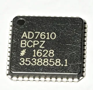
AD9228BCPZ-40 - Quad 12-bit 40 MSPS Serial LVDS ADC | Analog Devices
N.º da peça: AD9228BCPZ-40 ✓ Ativo| Qtd. | Preço unitário | Total |
|---|---|---|
| 1 | $32.5 | $32,50 |
| 10 | $29.25 | $292,50 |
| 100 | $25.75 | $2.575,00 |
| 500 | $22.95 | $11.475,00 |
| 1.000 | $20.5 | $20.500,00 |
AD9228BCPZ-40 Visão geral
An ADC (analog-to-digital converter) is a semiconductor device that converts continuous-time analog signals into discrete digital codes at a defined sample rate. The AD9228 belongs to the pipelined ADC family within the broader data-converter category, sitting between sigma-delta (high-resolution, low-speed) and SAR (medium-resolution, high-speed) converters. Quad ADCs are used when multiple channels must be sampled simultaneously - typically in medical imaging, communications base stations, and multi-antenna receivers - because integrated quad parts reduce board area, BOM cost, and channel-to-channel timing skew versus four discrete ADCs.
Key specifications include 70 dB SNR to Nyquist, 11.3-bit effective number of bits (ENOB), 82 dBc spurious-free dynamic range (SFDR) to Nyquist, ±0.3 LSB typical DNL and ±0.4 LSB typical INL. The -40 speed grade limits operation to 40 MSPS maximum; the higher-grade AD9228BCPZ-65 variant shares the same package and runs up to 65 MSPS. Programmable clock and data alignment plus built-in digital test pattern generation (deterministic, pseudo-random, and user-defined via SPI) simplify board bring-up and ATE test.
Typical applications include medical ultrasound beamforming receivers, multi-channel communications IF digitization, portable instrumentation, and multi-antenna software-defined radio front ends. The 1.8 V analog supply and LVDS digital interface minimize EMI and ease interface to modern FPGAs such as the Xilinx 7-series and Intel Cyclone families.
When designing with the AD9228, route analog inputs as 50 ohm differential pairs and place decoupling capacitors within 5 mm of each supply pin. Match trace lengths across the four channels when simultaneous sampling is required - the device's internal timing skew specification confirms the maximum acceptable mismatch budget.
This page synthesizes distributor pricing, drop-in alternative analysis, and practical design notes that are not aggregated on the manufacturer datasheet alone.
Alternativas drop-in para AD9228BCPZ-40 — mesmo encapsulamento, compatível pino a pino. Peças de encapsulamento diferente que exigem retrabalho na PCB são excluídas.
Variantes desta série
Modelos da mesma série compatíveis como drop-in com AD9228BCPZ-40 (mesmo formato e footprint) — diferindo em Analog Supply Voltage, ENOB, Input Type, Number of Channels, Package.
Ferramenta de comparação rápida — selecione peças alternativas para comparação lado a lado:
AD9228BCPZ-65
✅ Drop-In📋 Alternativa de referência (fora do catálogo)
AD9228ABCPZ-40
✅ Drop-In📋 Alternativa de referência (fora do catálogo)
AD9228BCPZRL7-40
✅ Drop-In📋 Alternativa de referência (fora do catálogo)
AD9228ABCPZRL7-40
✅ Drop-In✓ Em estoque
$21.4 / unidade
Ver ficha técnica →AD9228BCPZ-40 Classificações máximas e características elétricas
| Number of Channels | 4 (Quad) |
| Resolução | 12 bit |
| Sample Rate (max) | 40 MSPS |
| Architecture | Pipelined |
| Input Type | Differential |
| Analog Supply Voltage | 1.8 V (1.7 V to 1.9 V) |
| Digital Output Interface | Serial LVDS (ANSI-644) |
| Power Dissipation per Channel at 65 MSPS | 119 mW |
| SNR (to Nyquist) | 70 dB |
| ENOB | 11.3 bit |
| SFDR (to Nyquist) | 82 dBc |
| Encapsulamento | 48-LFCSP-VQ (7x7 mm) |
| Tipo de montagem | Surface Mount |
| Status RoHS | Compliant |
Guia de Configuração de Pinos do AD9228BCPZ-40 48-lfcsp-vq (7x7 mm)
Configuração de pinos para AD9228BCPZ-40 (pacote 48-lfcsp-vq (7x7 mm)). Este componente analógico possui pinos de entrada, saída e alimentação. Consulte o datasheet do fabricante para configurações de offset null, compensação e pino de enable. Ideal para circuitos de condicionamento de sinal e amplificadores.

Nenhum dado detalhado de pinagem disponível para AD9228BCPZ-40.
Consulte a ficha técnica para a configuração completa dos pinos.
Aplicações típicas
AD9228BCPZ-40 é adequado para 6 aplicaçãos: Medical Ultrasound Beamforming Receiver, Multi-Channel Communications IF Digitization, Multi-Antenna Software-Defined Radio Front End, Portable Industrial Instrumentation, Optical Coherence Tomography (OCT) Imaging, Multi-Channel Vibration Analysis.
Medical Ultrasound Beamforming Receiver
The AD9228BCPZ-40 is purpose-built for ultrasound receiver arrays requiring multiple analog channels sampled in phase coherence. Its quad-channel integration aligns the four on-chip sample-and-hold circuits to a shared clock, eliminating the channel-to-channel timing skew that would otherwise arise from four discrete ADCs. With 70 dB SNR and 82 dBc SFDR, the device resolves the small echo returns from deep tissue without saturating on strong surface reflections. The 40 MSPS sample rate comfortably captures ultrasound IF frequencies up to 20 MHz, and the serial LVDS output reduces FPGA pin count when scaling to 32-, 64-, or 128-element probe heads. Power consumption of 119 mW per channel at full throughput keeps total board dissipation manageable across large multi-channel systems.
Recomendado
Multi-Channel Communications IF Digitization
Cellular base-station receivers and software-defined radio platforms use the AD9228BCPZ-40 to digitize multiple intermediate-frequency (IF) signals simultaneously for digital downconversion in an FPGA or DSP. The quad 12-bit channels at 40 MSPS provide 70 dB SNR which is sufficient for narrowband signal demodulation in cellular and land-mobile-radio systems. The serial LVDS interface minimizes FPGA pin consumption when scaling from 4 to 64 channels, and the differential analog inputs reject common-mode noise from switching power supplies on the same board. Per-channel 119 mW power dissipation keeps thermal loading manageable in outdoor enclosures without active cooling. The exposed thermal pad on the 48-LFCSP-VQ package provides a low-thermal-resistance path to the PCB copper pour.
Recomendado
Multi-Antenna Software-Defined Radio Front End
Phased-array and MIMO receiver designs benefit from the AD9228BCPZ-40's four synchronized sample-and-hold channels, which preserve phase coherence across multiple antenna paths. The 11.3-bit ENOB and 82 dBc SFDR enable direction-finding algorithms to resolve weak signals in the presence of strong adjacent interferers. Serial LVDS output simplifies PCB routing to FPGAs performing beamforming, while 1.8 V single-supply operation eases power-tree design in portable SDR equipment. Differential analog inputs reject common-mode noise picked up across the antenna cabling, and the 48-LFCSP-VQ 7x7 mm footprint allows four or more ADCs to be placed close to the antenna feed network.
Recomendado
Portable Industrial Instrumentation
Handheld oscilloscopes, spectrum analyzers, and data-acquisition modules leverage the AD9228BCPZ-40 to digitize four channels in a single low-power IC. The 119 mW per channel power budget is critical for battery-powered instruments, where every milliwatt of dissipation reduces operating time. The 40 MSPS sample rate supports oscilloscope bandwidth up to 20 MHz in a compact handheld form factor, and the 12-bit resolution is sufficient for general-purpose signal integrity diagnostics in field service. The 48-LFCSP-VQ package's 7x7 mm footprint fits within dense multi-layer boards alongside FPGAs, displays, and battery management ICs.
Recomendado
Optical Coherence Tomography (OCT) Imaging
Swept-source OCT imaging requires multiple ADCs to capture interferometric signals from different depths simultaneously, and the AD9228BCPZ-40's four synchronized channels fit this requirement precisely. With 82 dBc SFDR, the device resolves the small OCT signal reflections in the presence of the large DC component from the reference arm. The 40 MSPS throughput accommodates 20 kHz A-scan rates when oversampling by 2x, and the serial LVDS output reduces FPGA pin count compared to parallel interfaces. Low per-channel power dissipation supports the small form factor of handheld OCT probes used in ophthalmology and dermatology.
Recomendado
Multi-Channel Vibration Analysis
Structural-health monitoring systems use the AD9228BCPZ-40 to digitize vibration signals from multiple accelerometers in bridges, turbines, and rotating machinery. The quad 12-bit channels at 40 MSPS capture vibration spectra up to 20 kHz with the SNR needed for accurate modal analysis. Differential analog inputs reject common-mode noise from motor drives and switching power converters in the same enclosure. The 1.8 V supply simplifies solar or battery-powered remote monitoring installations, and the 48-LFCSP-VQ package fits within the space-constrained sensor pods mounted on monitored equipment. Programmable digital test patterns via SPI simplify end-of-line calibration in production.
Recomendado
Resumo dos produtos recomendados
Dados de referência de engenharia para AD9228BCPZ-40 — comparação, orientação de projeto e informações de conformidade.
Guia de seleção
Comparação com alternativas
| Parâmetro | Este produto | AD9228BCPZ-65 | AD9228ABCPZ-40 | AD9228BCPZRL7-40 | AD9228ABCPZRL7-40 |
|---|---|---|---|---|---|
| Brand | Analog Devices | Analog Devices | Analog Devices | Analog Devices | Analog Devices |
| Package | 48-LFCSP-VQ (7x7) | 48-LFCSP-VQ (7x7) - same | 48-LFCSP-VQ (7x7) - same | 48-LFCSP-VQ (7x7) - same | 48-LFCSP-VQ (7x7) - same |
| Sample Rate (max) | 40 MSPS | 65 MSPS | 40 MSPS | 40 MSPS | 40 MSPS |
| Resolution | 12 bit | 12 bit | 12 bit | 12 bit | 12 bit |
| Number of Channels | 4 | 4 | 4 | 4 | 4 |
| SNR (to Nyquist) | 70 dB | 70 dB | 70 dB | 70 dB | 70 dB |
| SFDR (to Nyquist) | 82 dBc | 82 dBc | 82 dBc | 82 dBc | 82 dBc |
| Output Interface | Serial LVDS | Serial LVDS | Serial LVDS | Serial LVDS | Serial LVDS |
| Temperature Grade | Standard | Standard | Extended (A grade) | Standard | Extended (A grade) |
Principais diferenciais
- Quad 12-bit channel integration in a single 7x7 mm package (vs Discrete quad-ADC board designs)
- 70 dB SNR with 82 dBc SFDR at 40 MSPS (vs Lower-end 12-bit ADCs at 40 MSPS)
- Serial LVDS output with ANSI-644 compliance (vs Parallel CMOS output ADCs)
Notas de projeto
Route the four differential analog input pairs as 50 ohm impedance-matched microstrip or stripline, keeping trace lengths matched within 0.5 mm to preserve channel-to-channel phase coherence. Place the 0.1 µF and 10 µF decoupling capacitors within 5 mm of each AVDD and DRVDD pin, and connect the LFCSP-VQ exposed pad to a continuous ground plane using multiple thermal vias (typically 9 vias in a 3x3 grid). Ground plane splits beneath the analog input traces must be avoided to prevent coupling of digital switching noise into the sensitive analog front end.
Do not assume the -40 speed grade and -65 speed grade are interchangeable at the system level. While they share the same package and pinout, the FPGA LVDS receiver logic must tolerate the higher data rate when migrating to the -65 variant. Also note that LVDS termination (typically 100 ohm differential) must be placed at the FPGA receiver end, not at the ADC end. Failing to terminate LVDS properly results in reflections that degrade SFDR and may cause bit errors in the digitized output data stream across all four channels.
Estimated: Driving the ADC clock with a low-jitter clock source (jitter < 0.5 ps RMS) is required to preserve the 82 dBc SFDR rate. Higher jitter sources (e.g., recovered clocks from switching regulators or noisy FPGA outputs) will degrade SNR by approximately 20*log10(jitter/0.5 ps). When using a PLL to generate the ADC clock from a system reference, ensure the PLL loop bandwidth is set well above 1 MHz to avoid adding jitter at audio-band frequencies that would fall within the input signal passband.
Informações de conformidade
RoHS and REACH compliance per Analog Devices product page. Lead-free (Pb-free) confirmed. AEC-Q100 not applicable - this part is not automotive-qualified. Halogen-free status not explicitly stated in the datasheet snippet provided.