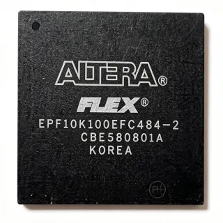
EP20K200CF484I8 - APEX 20KC FPGA 200K Gates 484-FBGA | Altera
N.º da peça: EP20K200CF484I8 ✗ Fim de vida| Qtd. | Preço unitário | Total |
|---|---|---|
| 1 | $785.16 | $785,16 |
| 10 | $706.65 | $7.066,50 |
| 50 | $628.13 | $31.406,50 |
| 100 | $549.61 | $54.961,00 |
| 250 | $471.1 | $117.775,00 |
EP20K200CF484I8 Visão geral
An FPGA (Field Programmable Gate Array) is a semiconductor integrated circuit built from an array of configurable logic blocks (CLBs), programmable interconnects, and embedded memory that can be re-programmed post-manufacturing to implement custom digital logic. APEX 20KC sits within the broader hierarchy: FPGA -> programmable logic device (PLD) -> logic IC -> semiconductor. The "20K" family combines Look-Up Table (LUT)-based logic with embedded CAM (Content Addressable Memory) and dual-port RAM, distinguishing it from older MAX CPLD families.
Key features include 8,320 logic elements, 26 embedded array blocks (EABs) for memory functions, four Phase-Locked Loops (PLLs) for clock management, and 4 LVDS channels for high-speed serial signaling. The device supports multiple I/O standards including LVTTL, LVCMOS, PCI, and LVDS. In-system programmability via IEEE 1149.1 JTAG and a built-in configuration scheme via EPC configuration devices enable flexible board-level integration.
Technical depth: The APEX 20KC architecture pairs coarse-grained embedded array blocks (EABs) for memory-intensive functions with fine-grained logic elements (LEs) for combinatorial logic, achieving an effective density of 200K system gates. MultiVolt I/O supports 1.8 V, 2.5 V, and 3.3 V interface voltages while the core runs at 1.8 V. The four on-chip PLLs multiply and divide incoming clocks while compensating for board-level skew, critical for synchronous designs above 100 MHz.
Typical applications include high-density ASIC prototyping, telecom backplane glue logic, industrial control and instrumentation, and DSP datapath co-processing where parallel arithmetic units outperform microcontrollers. The 376 user I/O pins make the device suitable for bus-intensive bridging functions. Design tip: APEX 20KC silicon has reached end-of-life status; plan for migration to Cyclone III/IV/V or Lattice ECP5 family with a Quartus II design retarget, as new design starts should target modern process nodes.
Alternativas drop-in para EP20K200CF484I8 — mesmo encapsulamento, compatível pino a pino. Peças de encapsulamento diferente que exigem retrabalho na PCB são excluídas.
Variantes desta série
Modelos da mesma série compatíveis como drop-in com EP20K200CF484I8 (mesmo formato e footprint) — diferindo em Package, Speed Grade, Process Technology, RoHS Status, Operating Temperature.
Ferramenta de comparação rápida — selecione peças alternativas para comparação lado a lado:
EP20K200CF484I7
✅ Drop-In✓ Em estoque
$89.5 / unidade
Ver ficha técnica →EP20K200CF484C9N
✅ Drop-In✓ Em estoque
$201.04 / unidade
Ver ficha técnica →EP20K200CF484C9
✅ Drop-In✓ Em estoque
$201.04 / unidade
Ver ficha técnica →EP20K200CF484C8N
✅ Drop-In✓ Em estoque
$102.95 / unidade
Ver ficha técnica →EP20K200CF484C8
✅ Drop-In✓ Em estoque
$410.75 / unidade
Ver ficha técnica →EP20K200CF484C7N
✅ Drop-In✓ Em estoque
$62 / unidade
Ver ficha técnica →EP20K200CF484I8 Classificações máximas e características elétricas
| Series | APEX 20KC |
| Family | APEX 20K |
| Logic Elements / Cells | 8320 |
| System Gates | 200,000 |
| Total RAM Bits | 106496 |
| Number of I/O | 376 |
| Voltage - Supply | 1.71 V to 1.89 V |
| Temperatura de operação | -40 C to +85 C (Industrial) |
| Encapsulamento / Caixa | 484-BBGA |
| Supplier Device Package | 484-FBGA (23x23 mm) |
| Tipo de montagem | Surface Mount |
| Packaging | Tray |
| Nível de sensibilidade à umidade (MSL) | 3 (168 Hours) |
| Process Technology | 0.15 micrometer CMOS |
| Internal Performance | 301.21 MHz |
Configuração de pinos do EP20K200CF484I8
| Pino 1 | I/O — User I/O pin (refer to datasheet ball map) |
| Pino 2 | I/O — User I/O pin |
| Pino 3 | I/O — User I/O pin |
| Pino 4 | I/O — User I/O pin |
| Pino 5 | I/O — User I/O pin |
| Pino 6 | I/O — User I/O pin |
| Pino 7 | VCCINT — Core supply voltage (1.8 V) |
| Pino 8 | I/O — User I/O pin |
| Pino 9 | GND — Ground |
| Pino 10 | I/O — User I/O pin |
Aplicações típicas
EP20K200CF484I8 é adequado para 6 aplicaçãos: ASIC Prototyping, Telecom Backplane Glue Logic, Industrial Control Systems, DSP Datapath Co-Processing, Test and Measurement Instrumentation, Legacy System Sustainment.
ASIC Prototyping
The EP20K200CF484I8's 200K system gates and 8,320 logic elements provide sufficient capacity for prototyping mid-complexity ASICs. The 106,496 bits of embedded RAM and 26 EABs enable realistic modeling of memory subsystems and bus interfaces. The industrial temperature grade allows prototyping of automotive and industrial ASICs. Compared to simulation, FPGA prototyping runs at MHz speeds for software validation and hardware-software co-verification.
Recomendado
Telecom Backplane Glue Logic
The 376 user I/O pins of the EP20K200CF484I8 are ideal for bus-intensive bridging functions on telecom backplanes where 32-bit and 64-bit parallel interfaces must be converted and buffered. The MultiVolt I/O supports 1.8 V, 2.5 V, and 3.3 V interface voltages, eliminating external level shifters. Four on-chip PLLs enable clock domain crossing between legacy and modern telecom fabrics.
Recomendado
Industrial Control Systems
With industrial temperature operation from -40 C to +85 C, the EP20K200CF484I8 suits PLC, motor control, and SCADA applications. The LVDS support and high I/O count enable multiple encoder, sensor, and communication interfaces to be aggregated in a single device. The 0.15 micrometer CMOS process provides robust electrical over-stress margin typical of industrial environments.
Recomendado
DSP Datapath Co-Processing
The 8,320 logic elements of the EP20K200CF484I8, combined with 26 EABs and 4 PLLs, allow implementation of parallel arithmetic units, FIR filters, and FFT datapaths that offload compute from a host DSP or microcontroller. The 301.21 MHz internal performance supports sample rates above 100 MHz in streaming DSP applications such as software-defined radio front ends.
Recomendado
Test and Measurement Instrumentation
The high I/O count of the EP20K200CF484I8 enables protocol-aware pattern generation for ATE and bench instruments. Integrated PLLs allow synthesis of multiple clock domains needed for legacy interface testing. The 106,496 bits of embedded RAM provide waveform buffering, and the JTAG IEEE 1149.1 boundary scan supports in-system testability of complex boards.
Recomendado
Legacy System Sustainment
The EP20K200CF484I8 is widely deployed in long-lifecycle defense, medical, and industrial systems where field replacement requires identical form-fit-function parts. Third-party distributors continue to hold residual inventory because active production has ended. For new designs, design teams should retarget to Cyclone III/IV/V families using Quartus II migration support to reduce long-term obsolescence risk.
Recomendado
Resumo dos produtos recomendados
Dados de referência de engenharia para EP20K200CF484I8 — comparação, orientação de projeto e informações de conformidade.
Guia de seleção
Comparação com alternativas
| Parâmetro | Este produto | EP20K200CF484I7 | EP20K200CF484C9N | EP20K200CF484C8N |
|---|---|---|---|---|
| Brand | Altera | Altera | Altera | Altera |
| Package | 484-FBGA (23x23) | 484-FBGA (23x23) | 484-FBGA (23x23) | 484-FBGA (23x23) |
| Logic Elements | 8320 | 8320 | 8320 | 8320 |
| Total RAM Bits | 106496 | 106496 | 106496 | 106496 |
| Number of I/O | 376 | 376 | 376 | 376 |
| Speed Grade | I8 (industrial) | I7 (industrial, slower) | C9 (commercial) | C8 (commercial) |
| Operating Temperature | -40 C to +85 C | -40 C to +85 C | 0 C to +85 C | 0 C to +85 C |
| Core Voltage | 1.71 V to 1.89 V | 1.71 V to 1.89 V | 1.71 V to 1.89 V | 1.71 V to 1.89 V |
| Lifecycle Status | NRND | NRND | NRND | NRND |
Principais diferenciais
- Industrial temperature grade with I8 speed grade (vs EP20K200CF484C8N)
- Higher internal performance than I7 speed grade (vs EP20K200CF484I7)
- Highest speed grade among same-package APEX 20K commercial variants (vs EP20K200CF484C9N)
Notas de projeto
The EP20K200CF484I8 requires a regulated 1.8 V core supply with tolerance of +/-5 percent (1.71 V to 1.89 V). Bypass each VCCINT pin with a 0.1 microfarad ceramic capacitor placed within 5 mm of the ball pad, plus a 10 microfarant tantalum bulk capacitor for each power plane. Use a dedicated PLL analog supply (VCC_PLL) filtered through a ferrite bead to minimize clock jitter. Estimated: total core current at 100 percent toggle rate approaches 1.5 A on a 200K-gate APEX 20K device; verify with PowerPlay early-stage estimator before finalizing power tree.
The 484-FBGA package requires thermal vias under the exposed die pad area to conduct heat to internal copper planes. Altera recommends a minimum 4-layer PCB with continuous VCCINT and GND planes directly beneath the device. For industrial temperature applications operating near +85 C ambient, place the device away from board-edge heat sources and provide at least 100 LFM of forced-air cooling. Estimated: junction-to-ambient thermal resistance theta_JA is approximately 14 C/W on a JEDEC JESD51-9 4-layer test board with thermal vias; thermal simulation is recommended for sealed enclosures.
Route all high-speed LVDS pairs with 100 ohm differential impedance and match trace lengths within 5 mils to maintain signal integrity. Place series-source terminators within 7 mm of the driver ball. The 1.0 mm ball pitch of the 484-FBGA demands 4 mil trace-and-space PCB fabrication; for finer 3.5 mil geometries, use laser-drilled microvias and HDI stack-up. JTAG chain integrity requires a 10 kilohm pull-up on TCK and TMS to keep the boundary scan interface in a benign state during board power-up.
APEX 20KC silicon is NRND and new production has ceased; do not start new designs on this device. Existing boards should plan a Quartus II retargeting to Cyclone IV E or Cyclone V family to avoid future obsolescence. PDF datasheet retrieval: the original Altera APEX 20K datasheet is archived on the Intel FPGA legacy documentation site; be aware that some third-party search results may mislabel APEX 20K and APEX 20KC device parameters, so always cross-reference the original document.
Informações de conformidade
RoHS, REACH, lead-free, and halogen-free status were not present in the verified distributor data. APEX 20KC silicon predates current RoHS transition and many variants are non-compliant; verify with the manufacturer before industrial use.