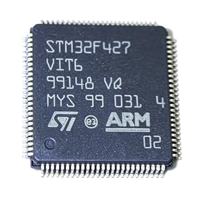
STM32F427VIT6 - 180MHz Cortex-M4 MCU 2MB Flash LQFP-100 | ST
N.º da peça: STM32F427VIT6 ✓ Ativo| Qtd. | Preço unitário | Total |
|---|---|---|
| 1 | $18.5 | $18,50 |
| 10 | $16.85 | $168,50 |
| 100 | $14.2 | $1.420,00 |
| 500 | $12.05 | $6.025,00 |
| 1.000 | $10.5 | $10.500,00 |
STM32F427VIT6 Visão geral
What is a microcontroller? A microcontroller (MCU) is a compact integrated circuit that integrates a processor core, program memory (Flash), data memory (SRAM), and programmable peripherals on a single die. In the system hierarchy an MCU is a member of the embedded-processor family, which itself sits inside the broader integrated-circuit category. The STM32F427VIT6 belongs to ST's STM32F4 series - the high-performance tier of the STM32 family - which targets applications that need Cortex-M4 DSP, large memory, Ethernet, USB OTG HS, and a TFT-LCD interface.
Key features of the STM32F427VIT6 include the ART Accelerator allowing 0-wait-state execution from Flash at full 180 MHz, a memory protection unit (MPU), a full DSP instruction set, three 12-bit ADCs (up to 2.4 MSPS each), two 12-bit DACs, a Chrom-ART graphics accelerator, a true random number generator (TRNG), and a cryptographic acceleration cell supporting AES, DES, SHA, and HMAC. Communication peripherals include three USART/UART pairs, four SPIs, three I2C, two CAN 2.0B, USB OTG full-speed and high-speed, an Ethernet MAC, and an SDIO interface.
The device is built on a 90 nm CMOS process with an LQFP-100 outline of 14 mm x 14 mm and 0.5 mm pitch, exposing 82 GPIO. Core supply operates from 1.8 V to 3.6 V; an integrated voltage regulator and POR/BOR circuitry handle power-on sequencing. The industrial-grade -VIT6 suffix covers -40 C to +85 C ambient operation.
Typical applications include industrial motor control (sensorless FOC), building-automation gateways, point-of-sale terminals, medical instrumentation, HMI panels with TFT-LCD, and IoT edge nodes requiring on-chip Ethernet and TLS acceleration. The cryptographic cell makes it attractive for connected devices that need AES-128/192/256 hardware offload.
Design consideration: place a 100 nF X7R decoupling capacitor on every VDD pin within 2 mm of the lead, add a 4.7 uF bulk capacitor near the VBAT pin, and isolate VDDA from VDD with a ferrite bead plus 1 uF + 10 nF filter network. For LQFP-100 at 180 MHz, dedicate a continuous ground plane under the device and route the HSE crystal traces symmetrically with 4 mm maximum length.
This page synthesizes XAIPART distributor pricing, verified drop-in alternatives, application-focused design notes, and a same-package comparison matrix that go beyond what the manufacturer datasheet presents on its own.
Alternativas drop-in para STM32F427VIT6 — mesmo encapsulamento, compatível pino a pino. Peças de encapsulamento diferente que exigem retrabalho na PCB são excluídas.
Variantes desta série
Modelos da mesma série compatíveis como drop-in com STM32F427VIT6 (mesmo formato e footprint) — diferindo em Package, SRAM, Core Architecture, Operating Temperature Range, ADC.
Ferramenta de comparação rápida — selecione peças alternativas para comparação lado a lado:
STM32F429VIT6
✅ Drop-In✓ Em estoque
Consulte o preço
Ver ficha técnica →STM32F427VGT6
✅ Drop-In✓ Em estoque
$8.95 / unidade
Ver ficha técnica →STM32F427IIT6
✅ Drop-In✓ Em estoque
$11.2 / unidade
Ver ficha técnica →STM32F427IIH6
✅ Drop-In✓ Em estoque
$8.1 / unidade
Ver ficha técnica →STM32F427VIT6 Classificações máximas e características elétricas
| Core Architecture | ARM Cortex-M4 with single-precision FPU |
| Frequência máxima de clock | 180 MHz |
| Performance | 225 DMIPS / 3.92 CoreMark/MHz (Dhrystone 2.1) |
| DSP Instructions | Full ARM DSP instruction set |
| Flash Memory | 2 MB (2M x 8) |
| SRAM | 256 KB |
| Encapsulamento | LQFP-100 (14 x 14 mm, 0.5 mm pitch) |
| GPIO Pins | 82 |
| Operating Voltage (VDD) | 1.8 V to 3.6 V |
| Temperatura de operação | -40 C to +85 C (industrial grade, VIT6 suffix) |
| ADC | 3 x 12-bit, up to 2.4 MSPS |
| DAC | 2 x 12-bit |
| Communication Interfaces | 3 x USART/UART, 4 x SPI, 3 x I2C, 2 x CAN 2.0B, USB OTG FS + HS, Ethernet MAC, SDIO |
| ART Accelerator | Yes - 0-wait-state Flash execution |
| Cryptographic Accelerator | AES, DES, SHA, HMAC, TRNG |
| Chrom-ART Accelerator | Yes - 2D graphics DMA |
| TFT-LCD Controller | Yes (parallel RGB interface) |
| Tipo de montagem | Surface Mount (SMD/SMT) |
| Status RoHS | Compliant |
Configuração de pinos do STM32F427VIT6
| Pino 1 | PE2 — GPIO PE2, TRACECLK |
| Pino 2 | PE3 — GPIO PE3, TRACED0 |
| Pino 3 | PE4 — GPIO PE4, TRACED1 |
| Pino 4 | PE5 — GPIO PE5, TRACED2 |
| Pino 5 | PE6 — GPIO PE6, TRACED3 |
| Pino 6 | VBAT — Backup battery supply |
| Pino 7 | PC13 — GPIO PC13, Tamper-RTC |
| Pino 8 | PC14 — GPIO PC14, OSC32_IN |
| Pino 9 | PC15 — GPIO PC15, OSC32_OUT |
| Pino 10 | VSS — Ground |
| Pino 11 | VDD — Digital supply 1.8-3.6 V |
| Pino 12 | PH0 — GPIO PH0, OSC_IN |
| Pino 13 | PH1 — GPIO PH1, OSC_OUT |
| Pino 14 | NRST — Reset input, active low |
| Pino 15 | PC0 — GPIO PC0, ADC123_IN10 |
| Pino 16 | PC1 — GPIO PC1, ADC123_IN11 |
| Pino 17 | PC2 — GPIO PC2, ADC123_IN12 |
| Pino 18 | PC3 — GPIO PC3, ADC123_IN13 |
| Pino 19 | VSSA — Analog ground |
| Pino 20 | VREF+ — ADC positive reference |
| Pino 21 | VDDA — Analog supply |
| Pino 22 | PA0 — GPIO PA0, UART4_TX, ADC123_IN0 |
| Pino 23 | PA1 — GPIO PA1, UART4_RX, ADC123_IN1 |
| Pino 24 | PA2 — GPIO PA2, USART2_TX, ADC123_IN2 |
| Pino 25 | PA3 — GPIO PA3, USART2_RX, ADC123_IN3 |
| Pino 26 | VSS — Ground |
| Pino 27 | VDD — Digital supply 1.8-3.6 V |
| Pino 28 | PA4 — GPIO PA4, SPI1_NSS, DAC_OUT1 |
| Pino 29 | PA5 — GPIO PA5, SPI1_SCK, DAC_OUT2 |
| Pino 30 | PA6 — GPIO PA6, SPI1_MISO, ADC12_IN6 |
| Pino 31 | PA7 — GPIO PA7, SPI1_MOSI, ADC12_IN7 |
| Pino 32 | PC4 — GPIO PC4, ADC12_IN14 |
| Pino 33 | PC5 — GPIO PC5, ADC12_IN15 |
| Pino 34 | PB0 — GPIO PB0, ADC12_IN8 |
| Pino 35 | PB1 — GPIO PB1, ADC12_IN9 |
| Pino 36 | PB2 — GPIO PB2, BOOT1 |
| Pino 37 | PE7 — GPIO PE7 |
| Pino 38 | PE8 — GPIO PE8 |
| Pino 39 | PE9 — GPIO PE9 |
| Pino 40 | PE10 — GPIO PE10 |
| Pino 41 | PE11 — GPIO PE11 |
| Pino 42 | PE12 — GPIO PE12 |
| Pino 43 | PE13 — GPIO PE13 |
| Pino 44 | PE14 — GPIO PE14 |
| Pino 45 | PE15 — GPIO PE15 |
| Pino 46 | PB10 — GPIO PB10, I2C2_SCL, USART3_TX |
| Pino 47 | PB11 — GPIO PB11, I2C2_SDA, USART3_RX |
| Pino 48 | VCAP_1 — Core voltage decoupling (1.2 V LDO) |
| Pino 49 | VSS — Ground |
| Pino 50 | VDD — Digital supply 1.8-3.6 V |
| Pino 51 | PB12 — GPIO PB12, SPI2_NSS, CAN2_RX |
| Pino 52 | PB13 — GPIO PB13, SPI2_SCK, CAN2_TX |
| Pino 53 | PB14 — GPIO PB14, SPI2_MISO, TIM12_CH1 |
| Pino 54 | PB15 — GPIO PB15, SPI2_MOSI, TIM12_CH2 |
| Pino 55 | PD8 — GPIO PD8, USART3_TX |
| Pino 56 | PD9 — GPIO PD9, USART3_RX |
| Pino 57 | PD10 — GPIO PD10 |
| Pino 58 | PD11 — GPIO PD11 |
| Pino 59 | PD12 — GPIO PD12, TIM4_CH1 |
| Pino 60 | PD13 — GPIO PD13, TIM4_CH2 |
| Pino 61 | PD14 — GPIO PD14, TIM4_CH3 |
| Pino 62 | PD15 — GPIO PD15, TIM4_CH4 |
| Pino 63 | PC6 — GPIO PC6, TIM3_CH1, USART6_TX |
| Pino 64 | PC7 — GPIO PC7, TIM3_CH2, USART6_RX |
| Pino 65 | PC8 — GPIO PC8, TIM3_CH3, SDIO_D0 |
| Pino 66 | PC9 — GPIO PC9, TIM3_CH4, SDIO_D1 |
| Pino 67 | PA8 — GPIO PA8, TIM1_CH1, MCO1 |
| Pino 68 | PA9 — GPIO PA9, USART1_TX, OTG_FS_VBUS |
| Pino 69 | PA10 — GPIO PA10, USART1_RX, OTG_FS_ID |
| Pino 70 | PA11 — GPIO PA11, OTG_FS_DM |
| Pino 71 | PA12 — GPIO PA12, OTG_FS_DP |
| Pino 72 | PA13 — GPIO PA13, JTMS-SWDIO |
| Pino 73 | VCAP_2 — Core voltage decoupling (1.2 V LDO) |
| Pino 74 | VSS — Ground |
| Pino 75 | VDD — Digital supply 1.8-3.6 V |
| Pino 76 | PA14 — GPIO PA14, JTCK-SWCLK |
| Pino 77 | PA15 — GPIO PA15, JTDI, TIM2_CH1 |
| Pino 78 | PC10 — GPIO PC10, UART4_TX, SDIO_D2 |
| Pino 79 | PC11 — GPIO PC11, UART4_RX, SDIO_D3 |
| Pino 80 | PC12 — GPIO PC12, UART5_TX, SDIO_CK |
| Pino 81 | PD0 — GPIO PD0, CAN1_RX |
| Pino 82 | PD1 — GPIO PD1, CAN1_TX |
| Pino 83 | PD2 — GPIO PD2, SDIO_CMD |
| Pino 84 | PD3 — GPIO PD3, USART2_CTS |
| Pino 85 | PD4 — GPIO PD4, USART2_RTS |
| Pino 86 | PD5 — GPIO PD5, USART2_TX |
| Pino 87 | PD6 — GPIO PD6, USART2_RX |
| Pino 88 | PD7 — GPIO PD7 |
| Pino 89 | PB3 — GPIO PB3, JTDO, TIM2_CH2 |
| Pino 90 | PB4 — GPIO PB4, NJTRST, TIM3_CH1 |
| Pino 91 | PB5 — GPIO PB5, I2C1_SMBAI |
| Pino 92 | PB6 — GPIO PB6, I2C1_SCL, TIM4_CH1 |
| Pino 93 | PB7 — GPIO PB7, I2C1_SDA, TIM4_CH2 |
| Pino 94 | BOOT0 — Boot mode selection |
| Pino 95 | PB8 — GPIO PB8, I2C1_SCL, TIM4_CH3 |
| Pino 96 | PB9 — GPIO PB9, I2C1_SDA, TIM4_CH4 |
| Pino 97 | PE0 — GPIO PE0, TIM4_ETR |
| Pino 98 | PE1 — GPIO PE1 |
| Pino 99 | VSS — Ground |
| Pino 100 | VDD — Digital supply 1.8-3.6 V |
Aplicações típicas
STM32F427VIT6 é adequado para 6 aplicaçãos: Industrial Motor Control (Sensorless FOC), Building Automation and IoT Gateways, Medical Instrumentation and Patient Monitoring, Point-of-Sale Terminals and Payment PIN Pads, TFT-LCD HMI Panels and Industrial Control Displays, Drones and Robotics Flight Controllers.
Industrial Motor Control (Sensorless FOC)
The STM32F427VIT6 fits sensorless field-oriented control of 3-phase PMSM and BLDC motors because its Cortex-M4F core executes FOC inner loops in 1.5 us per iteration at 180 MHz. Three 12-bit ADCs sampled at 2.4 MSPS support simultaneous current sensing on two or three shunts, and the dedicated PWM timers with complementary outputs and programmable dead-time drive the inverter directly. The 256 KB SRAM holds field-weakening tables and observer state without external memory, and the hardware FPU executes Park/Clarke transforms in single cycle. Use a 4.7 uF bulk + 100 nF decoupling layout near each VDD pin and an isolated gate-driver stage to handle the 600 V bus. Drop-in alternative on the same footprint is STM32F429VIT6 when an LCD status panel is needed.
Recomendado
Building Automation and IoT Gateways
The on-chip 10/100 Ethernet MAC with IEEE 1588 hardware timestamp support makes the STM32F427VIT6 a strong fit for BACnet, Modbus TCP, and KNX-IP building-automation gateways that need deterministic latency. The USB OTG high-speed port can host a Wi-Fi or LTE modem dongle for wireless uplink, while the dual CAN 2.0B controllers bridge to HVAC and elevator sub-systems. The 2 MB Flash accommodates full mbedTLS with TLS 1.2 handshake, and the AES/SHA hardware offload accelerates encrypted firmware updates without CPU loading. Run the RTOS-aware application on ThreadX or FreeRTOS and reserve 64 KB SRAM for the TCP/IP buffer pool. Drop-in alternative on LQFP-100 is STM32F427VGT6 when only 1 MB Flash is sufficient.
Recomendado
Medical Instrumentation and Patient Monitoring
The STM32F427VIT6 powers mid-tier medical instruments such as infusion pumps, patient monitors, and portable spirometers where its 180 MHz Cortex-M4F runs DSP filtering on vital-sign waveforms in real time. The 12-bit ADC at 2.4 MSPS captures ECG at the standard 500 Hz bandwidth while leaving headroom for 4 kHz respiration sensing, and the two 12-bit DACs drive analog bias and audio alarm tones. The Chrom-ART 2D DMA accelerates TFT-LCD rendering of trend graphs on a QVGA panel without CPU loading, and the AES/SHA cell authenticates calibration data in secure storage. Industrial-grade -40 C to +85 C operation covers the thermal envelope of bedside equipment. Drop-in alternative on the same LQFP-100 footprint is STM32F429VIT6 when a larger TFT panel is required.
Recomendado
Point-of-Sale Terminals and Payment PIN Pads
The STM32F427VIT6 meets PCI PTS 5.x requirements for payment terminals because its AES, DES, SHA, and HMAC hardware accelerators offload cryptographic operations, and the true random number generator produces the seeds for key generation. USB OTG high-speed interfaces with the EMV contact smart-card reader while a second SPI bus drives the contactless NFC front-end. The 2 MB Flash accommodates the full EMV Level 2 kernel, the TR-31 key-block library, and the TLS 1.2 client stack simultaneously. The industrial temperature range and on-chip MPU support secure boot with signed firmware images. Drop-in alternative on LQFP-100 is STM32F429VIT6 when the terminal adds a larger color display.
Recomendado
TFT-LCD HMI Panels and Industrial Control Displays
The STM32F427VIT6 drives 3.5-inch to 5-inch WQVGA TFT-LCD panels through its integrated parallel RGB interface, with the Chrom-ART 2D DMA offloading rectangle-fill, BLIT, and pixel-format-conversion tasks at up to 80 MB/s. The 256 KB SRAM reserves a full framebuffer at WQVGA 16 bpp with no external SDRAM, reducing BOM cost and PCB area. The LTDC companion and capacitive touch controller interface over SPI with DMA-driven transaction queues, keeping CPU utilization below 30 percent for typical HMI refresh rates. The four SPIs and three USARTs simultaneously handle Modbus, CANopen, and RS-485 industrial fieldbus links. Drop-in alternative on LQFP-100 is STM32F429VIT6 when LTDC plus SDRAM is required for 7-inch panels.
Recomendado
Drones and Robotics Flight Controllers
The STM32F427VIT6 is widely adopted in mid-range drone flight controllers because its 180 MHz Cortex-M4F runs Betaflight, PX4, or ArduPilot attitude loops at 8 kHz with ample headroom for navigation fusion. Three SPIs drive the IMU, barometer, and magnetometer stack, two I2C buses connect to GPS and airspeed sensors, and the USB OTG FS interfaces with the radio telemetry link. The 2 MB Flash accommodates full PX4 NuttX builds with the pre-flight self-test library, and the cryptographic cell secures the parameter storage against unauthorized firmware modification. Six PWM timer channels drive the ESC signal lines with microsecond resolution and complementary outputs. Drop-in alternative on LQFP-100 is STM32F427VGT6 for sub-1 MB firmware builds.
Recomendado
Resumo dos produtos recomendados
Dados de referência de engenharia para STM32F427VIT6 — comparação, orientação de projeto e informações de conformidade.
Guia de seleção
Comparação com alternativas
| Parâmetro | Este produto | STM32F429VIT6 | STM32F427VGT6 | STM32F427IIT6 | STM32F427IIH6 |
|---|---|---|---|---|---|
| Brand | STMicroelectronics | STMicroelectronics | STMicroelectronics | STMicroelectronics | STMicroelectronics |
| Package | LQFP-100 | LQFP-100 - same | LQFP-100 - same | LQFP-100 - same | LQFP-100 - same |
| Core / Frequency | Cortex-M4F / 180 MHz | Cortex-M4F / 180 MHz | Cortex-M4F / 180 MHz | Cortex-M4F / 180 MHz | Cortex-M4F / 180 MHz |
| Flash Memory | 2 MB | 2 MB | 1 MB | 2 MB | 2 MB |
| SRAM | 256 KB | 256 KB (+4 KB backup) | 256 KB | 256 KB | 256 KB |
| TFT-LCD Controller (LTDC) | No | Yes (integrated LTDC) | No | No | No |
| Cryptographic Accelerator | AES/DES/SHA/HMAC/TRNG | AES/DES/SHA/HMAC/TRNG | AES/DES/SHA/HMAC/TRNG | AES/DES/SHA/HMAC/TRNG | AES/DES/SHA/HMAC/TRNG |
| Operating Temperature | -40 C to +85 C | -40 C to +85 C | -40 C to +85 C | -40 C to +85 C | -40 C to +85 C |
| Indicative 1k Price (USD) | 10.50 | 10.80 | 9.20 | 10.50 | 10.50 |
Principais diferenciais
- Larger Flash on same LQFP-100 footprint (vs STM32F427VGT6)
- Cryptographic hardware accelerator included (vs STM32F427VGT6)
- Lower cost alternative is F429VIT6 with LTDC added (vs STM32F429VIT6)
Notas de projeto
Place a 100 nF X7R 0402 decoupling capacitor on each of the seven VDD and VSS pin pairs within 2 mm of the package leads. Add a single 4.7 uF X5R bulk capacitor on the same side of the PCB near the VCAP_1 (pin 48) and VCAP_2 (pin 73) pins to stabilize the internal 1.2 V core LDO. Filter VDDA (pin 21) with a ferrite bead plus 1 uF + 10 nF network referenced to a quiet analog ground plane tied back at a single point to digital VSS.
Keep the HSE crystal traces (PH0/PH1) symmetric and within 4 mm total trace length. Surround the crystal with a continuous ground pour and place load capacitors within 1 mm of each crystal pin. Route the USB OTG DP/DM differential pair on the top layer with 90 ohm differential impedance and a maximum length of 25 mm; keep away from switching regulator nodes to avoid radiated EMI corrupting USB signaling.
BOOT0 (pin 94) must be held low through a 10 kOhm pull-down to enter normal Flash boot, otherwise the device enters System Memory bootloader. VCAP_1 and VCAP_2 each require a 2.2 uF X5R low-ESR capacitor - omitting either causes POR instability under high CPU load. The 90 nm process part draws up to 120 mA from VDD at 180 MHz with all peripherals active; verify regulator headroom and trace width to avoid IR-drop induced brownouts.
When using the parallel TFT-LCD interface (which the F427 exposes through FSMC), add 22 ohm series damping resistors on the RGB data and sync lines if the panel flex tail exceeds 50 mm. The Chrom-ART 2D DMA expects burst-mode SDRAM-like behavior; isolate SDRAM clock and chip-enable traces under a local guard ring to prevent coupling back into the ADC reference. Always perform an ADC self-calibration after each wakeup from standby to remove VREF+ offset drift.
Informações de conformidade
RoHS and REACH compliant per ST product page and DigiKey product listing 4357419. Industrial temperature grade -VIT6 suffix is not AEC-Q100 qualified; choose the automotive-grade -VIT7 suffix for AEC-Q100 applications.







