АЦП/ЦАП
Товары (2518)
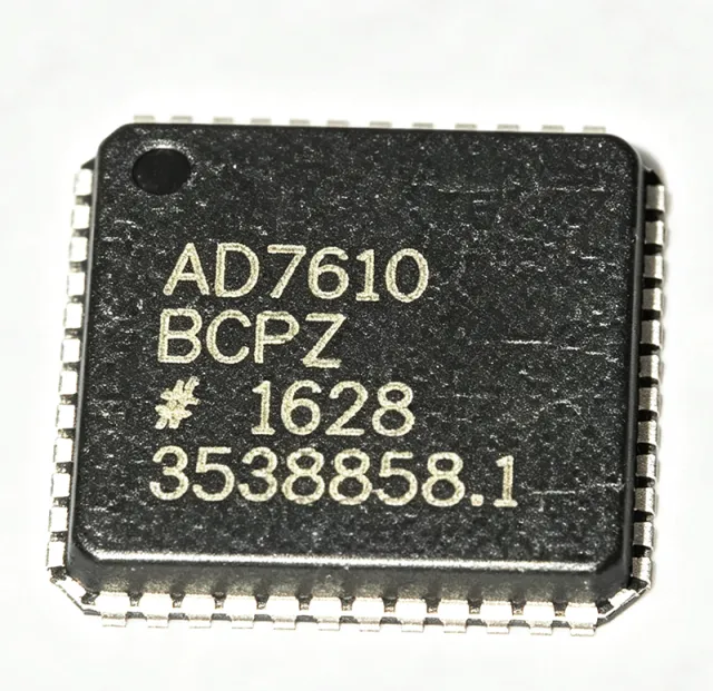
AD7610BCPZ-RL - 16-Bit 500kSPS SAR ADC | Analog Devices
The AD7610BCPZ-RL is a 16-bit charge redistribution successive approximation register (SAR) analog-to-digital converter (ADC) fabricated on Analog Devices' iCMOS high voltage process. It offers a maximum sampling rate of 500 kSPS and features a programmable input range supporting both unipolar and bipolar operation. The device is available in a 48-lead LFCSP-VQ (7x7 mm) package and is designed for high-performance data acquisition systems. An ADC (analog-to-digital converter) is an electronic component that converts continuous analog signals into discrete digital values. The AD7610 is a SAR ADC, which uses a binary search algorithm to determine the digital output, offering a good balance of speed, resolution, and power consumption. SAR ADCs are widely used in industrial, medical, and instrumentation applications where high accuracy and moderate sampling rates are required. Key features of the AD7610 include a 16-bit resolution, a maximum throughput of 500 kSPS, and a programmable input range that can be configured via hardware pins or a serial configuration port. The device operates from a single 5V analog supply and a 2.3V to 5.25V digital interface supply, making it compatible with a wide range of digital hosts. It also features a high-speed parallel and serial interface, allowing flexible connection to microcontrollers and DSPs. The AD7610 uses a charge redistribution architecture with an internal reference buffer, providing excellent linearity and low noise performance. The device includes an internal clock and can be configured for various operating modes, including normal, impulse, and fast modes, to optimize power consumption versus throughput. The iCMOS process enables high voltage operation while maintaining low power dissipation. Typical applications for the AD7610 include industrial process control, medical instrumentation, data acquisition systems, and automated test equipment. Its high resolution and programmable input range make it suitable for precision measurement applications where signal conditioning is required. When designing with the AD7610, it is important to provide adequate decoupling on the analog and digital supplies and to ensure a clean reference voltage for optimal performance. The device's input range should be configured to match the signal amplitude to maximize dynamic range.

AD7610BSTZ - 16-Bit 250kSPS SAR ADC | Analog Devices
The AD7610BSTZ is a 16-bit, 250 kSPS successive approximation register (SAR) analog-to-digital converter (ADC) from Analog Devices, fabricated on the iCMOS high voltage process. It features a unipolar/bipolar programmable input range, making it versatile for various data acquisition systems. The device is available in a 48-lead LQFP (7x7 mm) package and operates over the industrial temperature range. An ADC (analog-to-digital converter) is an electronic component that converts continuous analog signals into discrete digital numbers, enabling digital processing and storage. SAR ADCs use a binary search algorithm to approximate the input voltage, offering a good balance of speed, resolution, and power consumption. The AD7610 belongs to the PulSAR family, known for high accuracy and low power, and is part of the broader data converter hierarchy within mixed-signal ICs. Key features include a 16-bit resolution with no missing codes, a maximum throughput of 250 kSPS, and programmable input ranges of ±10 V, ±5 V, 0 to 10 V, and 0 to 5 V. It offers a parallel and serial interface, an internal reference, and a temperature range of -40°C to +85°C. The device also includes a busy indicator and a power-down mode for power-sensitive applications. The AD7610 uses a charge redistribution SAR architecture, which provides excellent linearity and low noise. The iCMOS process enables high voltage operation and reduces power consumption. The device includes an internal reference buffer and can operate with a 5 V analog supply and 2.3 V to 5.25 V digital supply, simplifying system design. Typical applications include industrial process control, data acquisition systems, medical instrumentation, and automated test equipment. The programmable input range allows direct interface to sensors with different output spans, reducing external signal conditioning. The high throughput and accuracy make it suitable for multi-channel multiplexed systems. When designing with the AD7610, ensure proper decoupling of the analog and digital supplies and a clean reference voltage. The input signal should be buffered to avoid charge injection errors. The parallel interface timing must be respected for reliable data transfer.

AD7610BSTZ-RL - 16-Bit 250kSPS PulSAR ADC | Analog Devices
The AD7610BSTZ-RL is a 16-bit, 250 kSPS successive approximation register (SAR) analog-to-digital converter (ADC) from Analog Devices, fabricated on the iCMOS high voltage process. It features programmable input ranges of ±10 V, ±5 V, 10 V, and 5 V, selectable via pins or a serial SPI-compatible port. The device operates from a 5 V analog supply and a 2.3 V to 5.25 V digital interface supply, with a typical power dissipation of 115 mW at 250 kSPS. It is available in a 48-lead LQFP (7x7 mm) package, with the -RL suffix indicating tape and reel packaging. A SAR ADC is a type of analog-to-digital converter that uses a binary search algorithm to convert an analog input into a digital output. It employs a comparator and a successive approximation register to iteratively narrow down the input voltage range, achieving high resolution and speed with low power consumption. SAR ADCs are widely used in data acquisition systems, industrial process control, and medical instrumentation where high accuracy and moderate sampling rates are required. Key features of the AD7610 include 16-bit resolution with no missing codes, a maximum throughput of 250 kSPS, and multiple programmable input ranges. The device offers a high-speed parallel interface and a serial SPI-compatible interface, providing flexibility in system integration. It also includes an internal reference buffer and supports external references, enabling precise voltage scaling. The iCMOS process ensures high voltage handling and low noise performance. The AD7610 architecture uses charge redistribution, which provides inherent sample-and-hold functionality and excellent linearity. The device includes a track-and-hold amplifier that captures the input signal, followed by a capacitive DAC that performs the successive approximation. This design achieves a typical signal-to-noise ratio (SNR) of 89 dB and a total harmonic distortion (THD) of -107 dB, making it suitable for high-precision measurement applications. Typical applications include industrial process control, data acquisition systems, medical instrumentation, and automated test equipment. The programmable input ranges allow direct interface with sensors and transducers without external scaling circuitry, simplifying design and reducing component count. The high input impedance and low power consumption make it ideal for battery-powered portable instruments. When designing with the AD7610, ensure that the analog input is properly buffered and that the reference voltage is stable and low-noise. The device requires a clean power supply with adequate decoupling to achieve optimal performance. The serial interface can be used to configure the input range and power-down modes, reducing power consumption in battery-operated systems.

AD7621ACPZRL - 16-Bit 3 MSPS PulSAR ADC | Analog Devices
The Analog Devices AD7621ACPZRL is a 16-bit, 3 MSPS, charge-redistribution successive approximation register (SAR) analog-to-digital converter that operates from a single 2.5 V power supply and is housed in a 48-lead LFCSP-VQ (7 mm x 7 mm) package with an exposed thermal pad. The integrated part combines a high-speed 16-bit sampling ADC, an internal conversion clock, and an internal reference buffer, supporting differential analog inputs with a ±VREF input range where VREF can be set up to 2.5 V. The device achieves a maximum INL of ±2 LSB (typical ±1 LSB), 89 dB SINAD and -101 dB THD at 100 kHz, and 16-bit resolution with no missing codes, all without pipeline delay thanks to its SAR architecture. An SAR ADC is a successive-approximation-register analog-to-digital converter that uses a binary-search algorithm and a charge-redistribution DAC to digitize a sampled analog input one bit per conversion clock. SAR ADCs sit at the next level of the converter hierarchy below delta-sigma and pipelined ADCs and are valued for their deterministic latency, single-shot accuracy, and lack of pipeline delay, which makes them well suited to multiplexed channel scanning, control loops, and event-driven sampling. The PulSAR family is Analog Devices' registered name for its precision, charge-redistribution SAR converter line. Key differentiating features include three selectable throughput modes (3 MSPS in wideband warp and warp modes, 2 MSPS in normal mode, and 1.25 MSPS in impulse mode), a 2.048 V internal reference, both serial and parallel (16- or 8-bit bus) digital interfaces, and a flexible input span driven by an external differential driver or AD8021/AD8138 driver. The warp mode and wideband warp mode further accelerate throughput by allowing faster acquisition at the cost of a tightened aperture window. Architecturally, the device pairs a high-bandwidth differential input track-and-hold with a precision charge-redistribution capacitive DAC and an on-chip conversion clock, which simplifies board-level timing. The single 2.5 V supply simplifies power-tree design, and the exposed-pad LFCSP-VQ package provides a low-thermal-resistance path to the PCB copper for heat spreading during continuous 3 MSPS operation. Typical application areas include medical imaging front-ends, industrial process control and data acquisition, instrumentation and automatic test equipment (ATE), and high-speed multichannel multiplexed systems. The 3 MSPS throughput and ±2 LSB INL are well aligned to imaging signal chains and to per-channel scanning modules behind a multiplexer. When designing in this ADC, allocate adequate ground and reference decoupling close to the pins, and lay out the analog input traces as a true differential pair terminated at the driver outputs. Use a low-jitter, low-phase-noise sampling clock to preserve aperture accuracy, and follow the AD7621 evaluation board layout for the LFCSP-VQ exposed pad to keep junction temperature within the rated -40 °C to +85 °C operating range. This page synthesizes verified distributor pricing, drop-in alternatives, and practical design notes not found in the manufacturer datasheet.
AD7621ASTZ - 16-Bit 3 MSPS SAR ADC | Analog Devices
The AD7621ASTZ is a 16-bit, 3 MSPS, charge redistribution successive approximation register (SAR) analog-to-digital converter (ADC) from Analog Devices. It operates from a single 2.5 V power supply and features a fully differential input, an internal conversion clock, and an internal reference buffer. The device is available in a 48-lead LQFP (7x7 mm) package, making it suitable for space-constrained industrial and medical applications. An ADC (analog-to-digital converter) is an electronic component that converts continuous analog signals into discrete digital values. The AD7621ASTZ belongs to the SAR ADC family, which uses a binary search algorithm to approximate the input voltage. SAR ADCs are known for their high speed, low power consumption, and excellent accuracy, making them ideal for applications requiring precise measurements at moderate sampling rates. The AD7621ASTZ is part of the PulSAR series, which is recognized for its high performance and reliability. Key features of the AD7621ASTZ include 16-bit resolution with 2 LSB integral nonlinearity (INL), a maximum sampling rate of 3 MSPS, and a fully differential input range of ±VREF. The device operates from a single 2.5 V supply, with an analog supply range of 2.37 V to 2.63 V, and features a serial and parallel interface for flexible data transfer. The internal conversion clock eliminates the need for an external clock, simplifying system design. The AD7621ASTZ uses a charge redistribution architecture that provides excellent linearity and low noise. The device includes an internal reference buffer, which reduces external component count and improves performance. The fully differential input allows for common-mode rejection, making it suitable for applications with noisy environments. The device also features a power-down mode to reduce power consumption when not converting. Typical applications for the AD7621ASTZ include medical imaging, high-speed data acquisition, industrial process control, and instrumentation. Its high speed and accuracy make it ideal for applications such as digital X-ray, ultrasound, and vibration analysis. The device's small package and low power consumption enable portable and battery-powered designs. When designing with the AD7621ASTZ, it is important to provide a clean, low-noise power supply and a stable reference voltage. The analog input should be driven with a low-impedance source to maintain accuracy. Proper decoupling of the power supply pins and careful PCB layout are essential to achieve the specified performance.
AD7621ASTZ-RL7 - 16-Bit 3MSPS PulSAR ADC | Analog Devices
The AD7621ASTZ-RL7 is a 16-bit, 3 MSPS, charge redistribution successive approximation register (SAR) analog-to-digital converter (ADC) from Analog Devices. It operates from a single 2.5 V power supply and features a fully differential input. The device is available in a 48-lead LQFP (7x7 mm) package, suitable for high-speed data acquisition systems. An ADC is an electronic component that converts an analog voltage or current into a digital number proportional to the magnitude of the signal. The AD7621 is a SAR-type ADC, which uses a binary search algorithm to determine the digital output. SAR ADCs are known for their high speed, low power consumption, and ease of use, making them ideal for applications requiring high-resolution sampling at moderate speeds. The AD7621 sits in the hierarchy of data converters, specifically within the family of high-speed, high-resolution ADCs used in industrial, medical, and communication systems. Key features of the AD7621 include a throughput of 3 MSPS in wideband warp and warp modes, 2 MSPS in normal mode, and 1.25 MSPS in impulse mode. It has an internal 2.048 V reference and supports a differential input range of ±VREF (with VREF up to 2.5 V). The device offers excellent linearity with 2 LSB INL (integral nonlinearity) and operates from a single 2.5 V supply, minimizing power consumption. The AD7621 also includes an internal conversion clock and a high-speed 16-bit sampling ADC, simplifying system design. Technically, the AD7621 uses a charge redistribution architecture that samples the analog input onto a capacitor array. The internal reference and conversion clock reduce external component requirements. The device provides both parallel and serial data interfaces, offering flexibility in system integration. The fully differential input provides common-mode rejection, improving noise performance in noisy environments. Typical applications for the AD7621 include high-speed data acquisition, medical imaging, instrumentation, and communication systems. Its high throughput and resolution make it suitable for applications such as digital oscilloscopes, spectrum analyzers, and industrial process control. The device's low power consumption and small package enable compact, portable designs. When designing with the AD7621, ensure proper decoupling of the power supply and reference pins. Use a low-noise reference and adequate analog input drive circuitry to achieve specified performance. The differential input should be driven with a suitable amplifier to maintain signal integrity.

AD7621BCPZ - 16-Bit 3 MSPS PulSAR ADC | Analog Devices
The AD7621BCPZ is a 16-bit, 3 MSPS, charge redistribution successive approximation register (SAR) analog-to-digital converter (ADC) from Analog Devices. It operates from a single 2.5 V power supply and features a fully differential input, an internal conversion clock, and an internal 2.048 V reference with a typical drift of ±7 ppm/°C. The device is available in a 48-lead LFCSP-VQ (7x7 mm) package, offering a compact solution for high-speed data acquisition systems. A SAR ADC is a type of analog-to-digital converter that uses a binary search algorithm to convert an analog input into a digital output. It is known for its high speed, low power consumption, and excellent accuracy, making it ideal for applications such as medical imaging, industrial process control, and instrumentation. The AD7621 belongs to the PulSAR family of ADCs, which are recognized for their superior linearity and low noise performance. Key features of the AD7621 include a 16-bit resolution with no missing codes, a maximum throughput of 3 MSPS, and a typical power dissipation of 65 mW. The device supports both parallel and serial output interfaces, providing flexibility in system design. The internal reference eliminates the need for an external reference, simplifying the design and reducing component count. The fully differential input allows for high common-mode rejection, improving noise immunity in noisy environments. The AD7621 is fabricated using Analog Devices' iCMOS high-voltage process, which enables high performance and reliability. The device includes an internal conversion clock, reducing the need for external timing components. The ADC operates over a temperature range of -40°C to +85°C, making it suitable for industrial applications. The LFCSP package provides excellent thermal performance and is RoHS compliant. Typical applications for the AD7621 include high-speed data acquisition systems, medical imaging equipment, industrial process control, and instrumentation. Its high throughput and accuracy make it ideal for applications requiring precise and fast analog-to-digital conversion. The device is also suitable for portable and battery-powered applications due to its low power consumption. When designing with the AD7621, it is important to provide a clean, low-noise power supply and proper decoupling to achieve optimal performance. The reference input should be bypassed with a capacitor to reduce noise. The digital interface should be designed to minimize crosstalk and ensure reliable data transfer.
AD7621BCPZ-RL7 - 16-Bit 3MSPS PulSAR ADC | Analog Devices
The AD7621BCPZ-RL7 is a 16-bit, 3 MSPS, charge redistribution successive approximation register (SAR) analog-to-digital converter (ADC) from Analog Devices. It operates from a single 2.5 V supply and typically dissipates only 65 mW, making it ideal for high-speed, low-power data acquisition systems. The device features a 2.048 V internal reference with a typical drift of ±7 ppm/°C, ensuring stable performance over temperature. It is available in a 48-lead LFCSP package (7x7 mm) and is specified over the industrial temperature range of -40°C to +85°C. A SAR ADC is a type of analog-to-digital converter that uses a binary search algorithm to convert an analog input into a digital output. It is known for its high speed, low power consumption, and excellent accuracy, making it suitable for applications such as medical imaging, industrial process control, and high-speed data acquisition. The AD7621 belongs to the PulSAR family of ADCs, which are renowned for their superior linearity and no missing codes. Key features of the AD7621 include a maximum throughput of 3 MSPS, no missing 16-bit codes, and an internal reference with low drift. The device also offers a flexible serial interface that is compatible with SPI, QSPI, MICROWIRE, and DSPs, simplifying integration into digital systems. The ADC operates from a single 2.5 V supply, reducing power supply complexity, and features a power-down mode for energy savings in battery-powered applications. The AD7621 uses a charge redistribution architecture with a capacitive DAC, providing excellent linearity and low noise. The internal reference buffer ensures accurate conversion results, while the device's high input bandwidth allows it to digitize high-frequency signals without significant aliasing. The ADC also includes a track-and-hold circuit that maintains signal integrity during conversion. Typical applications for the AD7621 include high-speed data acquisition, medical imaging (such as ultrasound and MRI), industrial process control, and instrumentation. Its combination of speed, accuracy, and low power makes it suitable for portable and battery-operated devices where power efficiency is critical. When designing with the AD7621, it is important to provide a clean, low-noise power supply and proper decoupling to achieve optimal performance. The reference voltage should be bypassed with a capacitor to minimize noise, and the analog input should be driven with a low-impedance source to avoid settling time issues.

AD7623ACPZRL - 16-Bit, 1.33 MSPS PulSAR ADC | Analog Devices
The Analog Devices AD7623ACPZRL is a 16-bit, 1.33 MSPS, charge-redistribution SAR (successive-approximation-register) analog-to-digital converter housed in a 48-lead LFCSP-VQ (7x7 mm) package with exposed pad. It operates from a single 2.5 V power supply and provides a fully differential analog input, integrating a high-performance front-end that combines low noise and wide input bandwidth for demanding precision acquisition. A SAR ADC is a successive-approximation-register analog-to-digital converter; it belongs to the broader class of Nyquist-rate data converters that sample an analog signal at a defined clock rate and resolve each sample to a binary code through a binary-search charge-redistribution DAC. The PulSAR architecture is a specific ADI family of SAR converters known for low-noise, low-power, high-precision operation, sitting within the hierarchy ADC -> data converter -> mixed-signal IC -> semiconductor. SAR ADCs are preferred over delta-sigma for multi-channel multiplexed and event-driven systems because they provide deterministic latency and no pipeline delay. Key features include a true 16-bit resolution with no missing codes, 1.33 MSPS throughput, low power consumption suitable for battery-powered industrial instruments, internal conversion clock, and a high-speed parallel or serial interface option. The fully differential input stage supports bipolar input ranges when biased around a common-mode voltage, and the wide input bandwidth preserves accuracy on fast transient signals. Typical applications include industrial process control, medical instrumentation, precision data acquisition systems, spectrum analysis, and portable battery-powered measurement front-ends. The wide input bandwidth and deterministic latency also suit multiplexed multi-channel systems where channels must be sampled in known phase relationships. When designing with the AD7623ACPZRL, select a low-noise, fast-settling driver amplifier such as the AD8021, as recommended in the AD7623 datasheet. Pay attention to PCB layout for the exposed pad - it must be soldered to a continuous ground plane to meet thermal and electrical performance, and decoupling should use ceramic capacitors placed as close as possible to the supply pins. This page synthesizes distributor pricing, drop-in alternatives, and practical design notes not found in the manufacturer datasheet alone, giving engineers a faster path from component selection to validated PCB implementation.
AD7623ASTZRL - 16-Bit 1.33 MSPS PulSAR ADC | Analog Devices
The Analog Devices AD7623ASTZRL is a 16-bit, 1.33 MSPS, charge redistribution SAR (successive approximation register) analog-to-digital converter housed in a 48-pin LQFP (Low-Profile Quad Flat Package) supplied on tape and reel. It operates from a single 2.5 V power supply, features a fully differential analog input, and integrates a 2.048 V internal reference with ±7 ppm/°C typical drift, removing the need for an external reference in most designs. The device supports both parallel and serial digital interfaces, allowing flexible host connectivity to DSPs, FPGAs, and microcontrollers. A SAR ADC is a type of analog-to-digital converter that uses a charge redistribution capacitive DAC combined with a comparator and successive-approximation logic to digitize an analog input in N clock cycles, where N equals the converter's resolution. SAR ADCs sit in the broader taxonomy of data converters (ADC -> Nyquist-rate ADC -> SAR ADC -> mixed-signal IC). Unlike delta-sigma ADCs, SAR converters offer single-shot latency, deterministic throughput, and no pipeline delay, which makes them ideal for multiplexing multi-channel systems and control loops where latency must be predictable. Key performance highlights include 1.33 MSPS throughput, 16-bit resolution with no missing codes, an excellent linearity profile, and a wide common-mode input range supported by the fully differential architecture. The AD8021 op amp is recommended by Analog Devices as the input driver because it settles cleanly at 16-bit levels at high gain. Combined with the 2.048 V internal reference, the AD7623 offers a high-accuracy single-supply solution for industrial instrumentation, medical imaging front-ends, and spectrum analysis systems. Typical applications include industrial process control and data acquisition, medical imaging (CT, ultrasound, MRI front-ends), spectrum analysis and vibration analysis, multi-channel multiplexed data acquisition systems, and precision instrumentation where deterministic latency matters. When designing with the AD7623, pay close attention to the input driver selection - the op amp must settle at 16-bit resolution (0.0015%) within the ADC acquisition time, not just at 0.1% or 0.01% which is more commonly published. Use a low-inductance ground plane and decouple the 2.5 V supply close to the pins. The LQFP-48 package has a typical θJA around 50 C/W; thermal rise is modest given the low supply current. This page synthesizes distributor pricing, drop-in alternatives within the PulSAR family, and design notes drawn from the Analog Devices AD7623 datasheet - content not consolidated on any single distributor page.
AD7634BCPZRL - 18-Bit 670kSPS Differential PulSAR ADC | Analog Devices
The Analog Devices AD7634BCPZRL is an 18-bit, 670 kSPS differential programmable input PulSAR successive approximation register (SAR) analog-to-digital converter housed in a 48-lead LFCSP-VQ (7x7 mm) package with exposed pad. It supports software- or pin-selectable true bipolar input ranges of ±10 V, 0 to 20 V, 0 to ±20 V, and ±40 V (10 V p-p through 40 V p-p) and offers both parallel and serial (SPI-compatible) data interfaces, allowing direct connection to DSPs, FPGAs, and microcontrollers. An SAR ADC is a successive-approximation converter that uses a binary-search algorithm and a precision DAC to digitize an input signal in N conversion cycles. PulSAR devices from Analog Devices are precision SAR ADCs that combine low noise, low power, and high throughput for industrial instrumentation. The AD7634 belongs to the precision data-converter family within Analog Devices' signal-chain portfolio, sharing heritage with the AD7621, AD7631, and AD7651 series, and targeting applications where bipolar signals and high dynamic range must be captured without front-end signal conditioning. Key features include 670 kSPS throughput, true bipolar differential inputs with software- or pin-programmable ranges, simultaneous sampling of two channels via the differential architecture, internal reference, internal clock, and pin-selectable serial or parallel digital output. The LFCSP-VQ-48 (7x7) package with exposed thermal pad provides low thermal resistance (junction-to-case) suitable for industrial temperature operation and reduces PCB footprint versus larger SOIC or LQFP alternatives. From an architecture standpoint, the device integrates a high-bandwidth differential input driver, a 32-tap digital filter, on-chip calibration logic, and a 2.5 V internal reference (with option to overdrive). The throughput-versus-INL curve and AC performance (SNR, SINAD) compete favorably with delta-sigma converters at Nyquist-rate bandwidths, while avoiding the latency penalty typical of sigma-delta devices. Typical applications include industrial process control (PLC analog input modules), power-line monitoring and protection relays, medical instrumentation (patient monitoring and diagnostic imaging front-ends), data acquisition systems for test and measurement, and multi-axis motor control feedback. According to Analog Devices product page, the 1ku starting list price is $48.81 (as of 2026-10-12). When designing with the AD7634BCPZRL, allocate adequate PCB copper area under the exposed pad to keep junction temperature within the -40C to +85C industrial range. Use the internal reference only when absolute accuracy below ±10 LSB is acceptable; otherwise overdrive REF with a low-noise external ADR435-class reference. Drive the analog inputs through low-impedance op-amp driver circuits (e.g., AD8021) to settle within the 670 kSPS acquisition window. This page synthesizes distributor pricing, drop-in same-package alternatives, and practical design notes not found on the manufacturer datasheet alone, providing engineering decision context for ADC selection in precision industrial designs.
AD7634BSTZRL - 18-Bit 670 kSPS PulSAR ADC | Analog Devices
The Analog Devices AD7634BSTZRL is an 18-bit, 670 kSPS successive-approximation (SAR) analog-to-digital converter (ADC) housed in a 48-pin LQFP package, supplied on tape and reel. The part combines high throughput with software- and pin-programmable input ranges (10 V p-p, 20 V p-p, 20 V p-p, and 40 V p-p) and offers both serial and parallel output interfaces for flexible system integration. Differential analog inputs use Analog Devices' PulSAR architecture for low noise and high DC accuracy. An SAR ADC is a converter class that resolves an analog input one bit per internal clock cycle using a switched-capacitor charge-redistribution DAC and a precision comparator. Compared with delta-sigma ADCs, SAR converters deliver single-cycle latency with no digital filtering delay, which makes them well suited to multiplexed data-acquisition front-ends and control loops. Within the broader taxonomy, the AD7634 belongs to precision data converters -> ADC -> SAR ADC -> integrated-circuit semiconductor, and it remains a workhorse in industrial and instrumentation signal chains where 16-18 bit DC accuracy and sub-microsecond settling are required. Key features of this AD7634 variant include selectable unipolar and bipolar input ranges via SPI-compatible serial mode control, throughput of 670 kSPS at 18-bit resolution, an internal 5 V reference option, and on-chip driver/receiver circuitry that simplifies interface to host microcontrollers, DSPs, or FPGAs. Differential inputs support high common-mode rejection, which is essential in noisy industrial environments. The wide dynamic input range, combined with low integral nonlinearity, makes the device a strong choice for process control and measurement. Typical applications include industrial process control, medical instrumentation, high-speed multiplexed data acquisition systems, spectrum analysis front ends, vibration and acoustic analysis, and automated test equipment. Designers select the AD7634 for applications where the combination of true 18-bit resolution, AC performance, and serial/parallel interface flexibility cannot be sacrificed. Designers should choose the appropriate input range at board-level using hardware pins or SPI commands to maximize dynamic range; select decoupling capacitors per the datasheet recommendation; and consider the digital-interface mode (parallel or serial) early in the architecture to minimize board rework. This page synthesizes distributor pricing, drop-in replacement alternatives and selection guidance not all available from a single manufacturer datasheet or distributor listing.
AD7641BCPZRL - 18-Bit 2MSPS PulSAR Bipolar ADC | Analog Devices
The Analog Devices AD7641BCPZRL is an 18-bit, 2 MSPS successive-approximation-register (SAR) analog-to-digital converter (ADC) built on Analog Devices' PulSAR iCMOS process technology, housed in a 48-pin LFCSP-VQ (7x7 mm) package. It supports software- or pin-programmable bipolar input ranges of ±10 V, ±5 V, and 0 V to 10 V (or 0 V to 5 V), making it well suited for industrial signal acquisition front-ends that accept high-voltage sensors directly without external attenuation. A SAR ADC is a successive-approximation-register analog-to-digital converter that performs a binary search against an internal DAC, producing a clean, single-conversion result with no pipeline latency. SAR ADCs occupy the same hierarchical slot as pipeline, sigma-delta, and flash converters within the data-converter product family, and within the broader integrated-circuit taxonomy they sit under ADC -> Data Converter -> Signal Chain IC -> Semiconductor. SAR parts are valued for deterministic latency, excellent DC accuracy, and ease of use in multiplexed multichannel systems. Key specifications include 18-bit resolution with ±1.75 LSB INL (≈7 ppm of full scale) and +2/-1 LSB DNL (no missing codes), a fast 2 MSPS throughput, true bipolar input capability with overvoltage-tolerant analog inputs, an internal 2.5 V reference (also usable as a low-noise external reference driver), and a high-speed parallel or serial SPI-compatible interface. The device operates from a single 2.5 V digital supply and a 5 V analog supply. Architecturally, the AD7641 integrates a high-impedance input front-end, a precision reference, the SAR core, and on-chip calibration logic; the iCMOS process allows 16 V input signal swing on a single 5 V supply. The high-throughput 2 MSPS rate and 18-bit linearity let engineers replace older bipolar-input ADCs that required external signal conditioning. Typical applications include industrial process-control PLC analog-input cards, power-line monitoring and protection relays, medical patient-monitoring front-ends, data-acquisition modules, and multichannel instrumentation systems. The bipolar ±10 V/±5 V ranges allow direct connection to ±10 V PLC analog-output cards and 4-20 mA loop sense resistors after shunt conversion. When designing with the AD7641BCPZRL, decouple the AVDD and DVDD rails separately, keep the input traces short and guarded, and follow the recommended reference bypass (10 µF + 100 nF) per the manufacturer datasheet to preserve 18-bit linearity. This page synthesizes distributor pricing, drop-in PulSAR-family alternatives, and practical PCB/calibration notes not found in the standalone manufacturer datasheet.
AD7650ACPZRL - 16-Bit 570kSPS SAR ADC | Analog Devices
The Analog Devices AD7650ACPZRL is a 16-bit, 570 kSPS successive approximation register (SAR) analog-to-digital converter with a single pseudo-differential input channel, offered in a 48-pin LFCSP-EP (7x7 mm) package and supplied on tape and reel. It supports both parallel and serial (SPI/QSPI/DSP-compatible) digital interfaces and operates from a single 5 V analog supply, drawing 77 mW typical in Warp Mode at 444 kSPS throughput. The ADC provides no pipeline delay, true bipolar input capability via the iCMOS high-voltage process, and an analog input range of 0 V to 2.5 V (unipolar) or ±2.5 V (bipolar) when paired with proper driver configuration. A successive approximation register (SAR) ADC is a precision data-acquisition converter that performs a binary search against the analog input using an internal capacitive charge-redistribution DAC, producing a conversion result in one cycle per bit with zero pipeline latency. SAR ADCs sit within the broader data-converter hierarchy of analog-to-digital converters, which themselves belong to the data acquisition and signal chain IC category. Compared with pipeline or delta-sigma ADCs, SAR architectures excel at multiplexed, multi-channel, single-shot and DC-precision measurements because each conversion is fully settled before the next sample begins. Key features of the AD7650 include 570 kSPS throughput in Warp Mode, 500 kSPS in Normal Mode, 16-bit resolution with no missing codes, an internal 2.5 V reference, throughput-scalable power dissipation (77 mW at full speed down to 21 µW at 100 SPS), and hardware-configurable input ranges. The LFCSP-48 package with exposed pad (EP) keeps theta_JA low for reliable operation across the -40°C to +85°C industrial temperature range. Architecturally, the AD7650 uses Analog Devices' iCMOS process to combine high-voltage bipolar input ranges with low-voltage CMOS logic on a single die. The integrated S/H front-end, precision reference, and flexible digital interface (parallel word or serial SPI/QSPI/DSP) make it a turnkey solution for industrial control loops, power-line monitoring and multi-axis data acquisition systems. Typical applications include industrial process control (PLC analog input modules), multi-axis motor control position feedback, power-line monitoring and protective relaying, data acquisition boards for medical and instrumentation equipment, and high-speed multiplexed signal acquisition. The flexible interface allows direct connection to DSPs, FPGAs and microcontrollers without external glue logic. When designing with the AD7650, ensure the exposed die leads are bonded or the exposed pad is soldered to a sufficiently large copper pour to maintain the published thermal resistance; bypassing it, especially for high-throughput industrial-grade operation, will compromise long-term reliability. Use the parallel interface for highest sample rates and the serial interface for space-constrained designs with isolation barriers. This page synthesizes verified distributor pricing, drop-in alternative MPNs from the ADI SAR portfolio, and practical design notes that go beyond the integrated information typically available from distributor catalog listings.
AD7651ACPZRL - 16-Bit 100kSPS PulSAR ADC | Analog Devices
The Analog Devices AD7651ACPZRL is a 16-bit, 100 kSPS successive-approximation register (SAR) analog-to-digital converter (ADC) with integrated reference, supplied in a 48-lead LFCSP-VQ (7x7 mm, MO-220-VKKD-2) surface-mount package. It operates from a 5V analog supply and supports a true bipolar or unipolar input range of 0V to 2.5V on a single channel, with throughput rates up to 100,000 samples per second. The device combines a charge-redistribution SAR core with an on-chip reference and a high-speed parallel/serial interface. A SAR ADC is a successive-approximation register analog-to-digital converter that uses a binary-search charge-redistribution architecture to resolve each conversion in N clock cycles for an N-bit result. The architecture delivers deterministic latency, low power dissipation, and excellent dynamic performance at moderate sample rates, making SAR converters the category of choice for multiplexed data acquisition, motor control, and industrial instrumentation where the converter sits within the broader signal chain of sensor -> signal conditioning -> ADC -> MCU/DSP -> communication. Key features include ±15V input overvoltage protection on the analog inputs, on-chip 2.5V reference with low 5 ppm/°C typical temperature drift, 84 dB SNR at 10 kHz input, and selectable bipolar (±5V, ±10V) or unipolar (0-2.5V, 0-5V, 0-10V) input ranges via hardware pin strapping. The LFCSP-48 7x7 footprint provides a thermal pad that lowers junction-to-PCB thermal resistance and supports the ±10V true-bipolar input configuration directly from ±15V rails without external protection. Typical applications include industrial process control (PLC analog input modules), power-line monitoring, multi-axis motor control current sensing, and portable instrumentation. The AD7651ACPZRL's combination of bipolar input range, on-chip reference, and parallel interface simplifies board layout compared to discrete ADC + external reference + amplifier signal chains. When designing with this part, observe the recommended 10uF + 0.1uF decoupling network on each supply pin and route the analog and digital ground planes as a single star-grounded split to preserve 84 dB SNR.
AD7651ASTZRL - 16-Bit 100kSPS PulSAR Unipolar ADC | Analog Devices
The Analog Devices AD7651ASTZRL is a 16-bit, 100 kSPS successive approximation register (SAR) analog-to-digital converter with integrated reference, packaged in a 48-pin LQFP (7 mm × 7 mm) and shipped on tape and reel. As a member of the PulSAR unipolar ADC family, it combines charge-redistribution SAR architecture with a wide ±10 V or 0–5 V true bipolar/unipolar input range through Analog Devices' iCMOS high-voltage process technology. The integrated 2.5 V reference, low noise floor, and 100 kSPS throughput make it a strong fit for industrial data acquisition and process control front-ends. A successive approximation register ADC is a precision data converter that resolves one bit per conversion cycle using an internal DAC and comparator; SAR ADCs deliver deterministic latency, no-pipeline-delay sampling, and inherently low noise because quantization noise is not folded into the baseband. The SAR architecture sits within the data-converter hierarchy of analog-to-digital converters -> ADCs -> precision ADCs -> successive approximation ADCs -> industrial ADCs, and the integrated reference places this part in the power management-adjacent category of self-contained analog front-ends. Key features of the AD7651ASTZRL include 16-bit resolution with no missing codes, 100 kSPS throughput, an integrated low-drift reference, both serial and parallel interface options, and a wide input voltage range supporting true bipolar ±10 V or unipolar 0 V to 5 V operation directly from ±12 V or +5 V supplies. The device also provides flexible power management through per-channel logic, hardware gain compression at PGA=2, and low power consumption of 8 mW typical at 100 kSPS. Typical applications include industrial process control and PLC analog input modules, multi-channel data acquisition systems, portable or battery-powered instrumentation, and power-line monitoring where ±10 V signals must be digitized directly. The wide input range eliminates the need for front-end signal conditioning in many 4–20 mA or ±10 V transducer scenarios. When designing with this device, ensure the AVCC and DVDD rails are properly decoupled with 10 uF tantalum and 100 nF ceramic capacitors as recommended in the manufacturer datasheet, and verify that the REF decoupling (10 uF/100 nF) is placed close to the REF pin to preserve linearity at full throughput.
AD7652ASTZRL - 16-Bit 500kSPS SAR ADC | Analog Devices
The Analog Devices AD7652ASTZRL is a 16-bit, 500 kSPS successive approximation register (SAR) analog-to-digital converter with a parallel/serial data interface, a 2.5 V internal reference, and a unipolar analog input range. Housed in a 48-pin LQFP package, the part is supplied on a 13-inch tape-and-reel format suitable for high-volume SMT production. The device integrates a high-speed SAR core, on-chip reference, and a versatile digital interface, simplifying data-acquisition front ends that previously required a separate ADC plus external reference. What is a SAR ADC? A successive-approximation-register analog-to-digital converter is a sampling ADC architecture that uses a binary-search algorithm against an internal DAC to resolve each analog sample into N bits. SAR ADCs trade the multi-megasample speeds of pipeline ADCs for excellent DC accuracy, low latency, and very low power consumption - making them the architecture of choice for industrial process control, instrumentation, and multi-channel data-acquisition systems where linearity and noise immunity are more important than absolute conversion rate. Key features of the AD7652 include 500 kSPS throughput, ±2 LSB INL (typical) at 16 bits, a true bipolar-capable analog input structure, a hardware-/software-controlled power-down mode, and a flexible digital interface supporting both parallel and serial (SPI/QSPI/MICROWIRE/DSP-compatible) readback. The on-chip 2.5 V reference is trimmed to ±0.2% (typical) and is also accessible externally, allowing the part to reference other circuit blocks while simultaneously serving the ADC core. The analog supply (AVCC) accepts 4.75 V to 5.25 V, and the digital supply (DVCC) accepts 2.7 V to 5.25 V, simplifying interfacing to 3.3 V and 5 V logic families. The internal architecture pairs a charge-redistribution DAC with a dedicated comparator and SAR logic clocked from an on-chip oscillator. Analog input is sampled through a true bipolar front end that accepts 0 V to 5 V (unipolar mode) or ±10 V / ±5 V / 0 to 10 V ranges when configured with the appropriate front-end scaling resistors. This eliminates, in many applications, the external signal-conditioning amplifier that would otherwise sit between sensor and ADC. Typical applications include industrial process control (PLC analog input modules), multi-axis motor control position feedback, medical instrumentation front ends, weigh-scale and strain-gauge digitizers, and general-purpose multi-channel data-acquisition boards. In motor-control loops the 500 kSPS rate and deterministic latency allow phase currents to be sampled coherently with the PWM carrier. In power-quality monitoring, the simultaneous-sample-with-track-and-hold combination on the AD7652 enables accurate capture of transient waveforms without external sample-and-hold circuitry. When designing with the AD7652, ensure the analog input is driven from a low-impedance source - typical 20 ohms or less - so that the 575 pF input capacitance settles within the acquisition window. Use a 4.7 nF ceramic decoupling capacitor on each AVCC pin placed within 5 mm of the package, and keep the analog and digital grounds joined at a single star point beneath the exposed pad of the LQFP. This page synthesizes distributor pricing, drop-in alternatives, and practical design notes not found in the manufacturer datasheet, providing engineers with an at-a-glance view of how the AD7652ASTZRL compares to its closest pin-compatible peers.
AD7653ASTZRL - 16-Bit 1 MSPS SAR ADC | Analog Devices | LQFP-48
The Analog Devices AD7653ASTZRL is a 16-bit, 1 MSPS successive-approximation register (SAR) analog-to-digital converter that integrates a precision reference, sample-and-hold amplifier, and high-speed parallel/serial digital interface into a 48-pin LQFP package. The device operates from a single 5V analog supply, accepts a unipolar 0V-to-VREF /-VES analog input range, and offers no pipeline delay thanks to its SAR architecture. What is a SAR ADC? A successive-approximation register analog-to-digital converter is a precision data converter that resolves the input voltage through a binary search using a single comparator and a switched-capacitor DAC. Compared to pipeline ADCs, SAR converters offer zero latency (true single-shot conversion), deterministic behavior, and excellent DC accuracy with low power consumption, which makes them ideal for multiplexed data acquisition, industrial process control, and precision instrumentation. Within the broader signal-chain taxonomy, a precision SAR ADC sits above general-purpose 12-bit ADCs but below 18/24-bit delta-sigma converters in resolution, trading oversampling for single-cycle latency. Key features include 16-bit resolution with no missing codes, throughput of 1 MSPS in Warp mode (800 kSPS Normal, 666 kSPS Impulse), internal 2.5V reference, on-chip reference buffer, software-configurable analog input ranges (0V to VREF / 0V to 2×VREF), and selectable parallel or serial interface. The integrated reference eliminates external reference noise pickup and simplifies BOM. The pulSAR core delivers typical INL of ±1 LSB and SNR of 86 dB, supporting demanding measurement bandwidths. Architecturally, the AD7653 uses ADI's proprietary pulSAR switching technique that minimizes input transient currents and allows direct connection to high-impedance front-ends with minimal settling time. Power dissipation is 25 mW at 1 MSPS, scaling linearly with throughput - a major efficiency advantage over continuously-sampling converters. The device supports hardware/software configurable input ranges and provides an internal clock option. Typical applications include industrial process control (PLC analog front-ends), multichannel data acquisition systems, precision weigh scales, instrumentation and medical imaging front-ends, and digital oscilloscope input stages. The combination of true 16-bit accuracy, internal reference, and zero pipeline delay suits closed-loop control loops where each sample must be acted upon in real time. When designing with this device, ensure adequate input RC anti-alias filtering, place the AVCC decoupling capacitors as close as possible to the supply pins, and route the AGND/DGND grounds as a star at the device. Compared to discrete ADC + external reference designs, the integrated reference reduces long-term drift and improves thermal stability across the -40C to +85C industrial range. This page synthesizes distributor pricing, drop-in alternatives, and practical design notes not found in the manufacturer datasheet.
AD7655ACPZRL - 16-Bit 1MSPS 4-Ch SAR ADC | Analog Devices
The Analog Devices AD7655ACPZRL is a low-cost, 4-channel, 16-bit, 1 MSPS successive-approximation analog-to-digital converter (SAR ADC) housed in a 48-lead LFCSP-VQ (7x7 mm) package with an exposed thermal pad. Per the Analog Devices AD7655 datasheet, it delivers 1 MSPS throughput in normal mode and 888 kSPS in impulse mode, with bipolar or unipolar input ranges spanning ±10 V, 0 V to 5 V, and ±5 V. A successive-approximation register ADC is a converter architecture that performs bit-by-bit trial conversions using an internal DAC, comparator, and successive-approximation register, achieving low latency and deterministic behavior compared to pipelined or delta-sigma converters. The AD7655 belongs to the PulSAR family of precision SAR ADCs from Analog Devices, sitting within the broader iCMOS (industrial CMOS) high-voltage process family and the company's mixed-signal data-converter product line. Key features include dual track-and-hold amplifiers that allow simultaneous sampling of two channels, true 16-bit resolution with no missing codes, no pipeline delay inherent to its SAR architecture, parallel or serial (SPI/QSPI/MICROWIRE/DSP-compatible) digital interface, and an operating temperature range of -40C to +85C. Per the manufacturer datasheet, the part accepts a 5 V analog supply and operates from a flexible digital supply. Typical applications include multi-channel data acquisition systems, industrial process control, instrumentation, motor control feedback loops, and medical monitoring equipment. Its four simultaneous-sampling channels make it a natural fit for three-phase power monitoring, vibration analysis, and any polyphase measurement requiring synchronized conversion of multiple analog signals at high resolution. When designing with the AD7655ACPZRL, place 10 uF tantalum and 100 nF ceramic bypass capacitors as close as possible to the AVDD and DVDD pins, and ensure the exposed thermal pad is soldered to a continuous analog ground plane for thermal dissipation and low-impedance analog return. Driver amplifier selection matters: per the AD7655 datasheet, the 16-bit settling time must be verified before choosing an external op amp, as 0.1% or 0.01% settling specifications from amplifier datasheets can differ significantly from 16-bit (0.0015%) settling. This page synthesizes distributor pricing across DigiKey, Mouser, and authorized partners, drop-in alternatives within the ADI PulSAR family, and practical layout guidance that extends the manufacturer datasheet with engineer-focused perspective.

AD7656YSTZ-1-RL - 16-Bit, 250kSPS 6-Ch Bipolar ADC | ADI
The Analog Devices AD7656YSTZ-1-RL is a 16-bit, 250 kSPS, 6-channel simultaneous-sampling successive-approximation ADC with true bipolar analog inputs, packaged in a 64-pin LQFP (ST-10x10). It is the tape-and-reel, reduced-decoupling variant of the AD7656-1 family, manufactured on Analog Devices' iCMOS (industrial CMOS) process for low power and high precision. What is a successive-approximation ADC (SAR ADC)? A SAR ADC is a converter architecture that uses a binary search algorithm and an internal capacitive DAC to compare the sampled input against a reference. Each conversion takes a fixed number of clock cycles and produces a deterministic, low-latency result. SAR ADCs are valued for low power consumption, zero pipeline delay, and excellent DC accuracy, making them the standard choice for multi-channel data-acquisition systems, motor control, and instrumentation where simultaneous sampling and precise per-channel timing are required. Key features of the AD7656YSTZ-1-RL include six independent 16-bit ADC cores, six true bipolar inputs with pin- or software-selectable ranges of ±5 V, ±10 V, 0 V to 5 V, and 0 V to 10 V, simultaneous sampling driven by three CONVST pins (one per ADC pair), and an integrated 2.5 V on-chip reference. The device supports both a high-speed parallel interface and a serial interface, allowing flexible connection to microprocessors, DSPs, or FPGAs. Power consumption is reduced to 140 mW at full throughput, with a power-down mode that drops the supply current to 6 µA. Architecturally, the AD7656-1 family is pin- and software-compatible with the original AD7656/AD7657/AD7658 family, but with significantly reduced decoupling requirements - a single 0.1 µF capacitor on each AVCC is sufficient. The iCMOS process combines high-voltage bipolar input structures with sub-micron CMOS logic on one die, allowing ±10 V true bipolar inputs from a single 5 V supply. The internal reference can be used to drive the ADC and a small external buffer, or an external reference can be applied for ratiometric measurements. Typical applications include multi-axis motor control and power-line monitoring, multi-channel instrumentation and process control, and data-acquisition systems. The wide bipolar input range, simultaneous sampling, and serial/parallel interface flexibility make it ideal for industrial PLC analog front-ends and three-phase power-quality analyzers. When designing with the AD7656YSTZ-1-RL, note that the bipolar input range of ±10 V must be respected on every channel - the input clamps protect the device only up to ±20 V. Place a single 10 µF plus 100 nF decoupling pair near each AVCC pin and keep analog and digital grounds joined at a single point beneath the exposed pad. This page synthesizes distributor pricing, drop-in alternatives, and practical design notes not found in the manufacturer datasheet.
AD7657YSTZ-REEL - 14-Bit 6-Ch 250 kSPS Bipolar ADC | Analog Devices
The Analog Devices AD7657YSTZ-REEL is a 14-bit, 6-channel, simultaneous-sampling successive-approximation analog-to-digital converter (SAR ADC) housed in a 64-pin LQFP (10x10 mm) package, qualified for automotive temperature grades (-40C to +125C) and supplied on a 7-inch reel. It delivers a per-channel throughput of 250 kSPS from six independent ADCs sharing one package, with true bipolar analog inputs and pin-/software-selectable input ranges of +/-5V, +/-10V and 0-5V/0-10V. The device is fabricated on Analog Devices' iCMOS (industrial CMOS) process, which combines high-voltage silicon with submicron CMOS and complementary bipolar transistors to deliver the high analog input ranges of +/-10V or +/-5V from a single 5V supply. A successive-approximation ADC is a converter architecture that uses a binary-search algorithm against an internal precision DAC to digitize an analog input in N clock cycles, where N is the resolution. SAR ADCs are prized for their deterministic latency, lack of pipeline delay, and excellent DC accuracy, which is why they dominate multi-channel data-acquisition front ends where phase coherence between channels matters. The AD7657's six independent SAR cores, paired with three CONVST pins, allow simultaneous sampling of three ADC pairs - a critical capability for three-phase power, motor control and vibration analysis. The bipolar +/-10V input range, single 5V supply, low power consumption at 250 kSPS and simultaneous sampling across six channels make this ADC ideal for industrial automation, motor control, multi-axis vibration monitoring and power-line monitoring. The high-speed parallel and serial interface can be connected to microprocessors or DSPs without external signal conditioning. When designing with the AD7657, pay close attention to the analog input anti-alias filter: each of the six channels requires its own RC network sized for the desired input bandwidth. Also note that the bipolar input range is achieved by on-chip attenuation and level shifting, so the source impedance must remain below the value recommended by the datasheet to preserve linearity.
AD7658YSTZ-REEL - 12-Bit 250 kSPS 6-Ch Simultaneous-Sampling ADC | Analog Devices
The Analog Devices AD7658YSTZ-REEL is a 12-bit, 250 kSPS, 6-channel, simultaneous-sampling, bipolar-input successive-approximation ADC housed in a 64-pin LQFP (10x10 mm) package. It integrates six independent SAR ADCs on a single die using the proprietary iCMOS (industrial CMOS) process, which combines high-voltage silicon with submicron CMOS and complementary bipolar technologies. Each ADC channel features true bipolar analog inputs with pin- or software-selectable input ranges of ±10 V or ±5 V, and the device achieves 86.5 dB SNR at 50 kHz input frequency. An analog-to-digital converter (ADC) is a data acquisition component that converts continuous analog signals into discrete digital codes for processing by microcontrollers, DSPs, or FPGAs. Successive-approximation register (SAR) ADCs are valued for their deterministic latency, low power, and high DC accuracy, making them a mainstay in industrial measurement, instrumentation, and motor-control signal chains. The AD7658YSTZ-REEL sits at the top of the SAR hierarchy: 6 independent SAR cores -> multi-channel SAR ADC -> data acquisition IC -> signal chain -> mixed-signal system. A simultaneous-sampling architecture is critical for three-phase power, polyphase vibration, and any application that requires per-channel phase alignment. Key differentiating features include six independent ADC cores (not multiplexed), true bipolar ±10 V / ±5 V inputs that accept industrial signal levels directly without external signal conditioning, an integrated 2.5 V on-chip reference with reference buffers to reduce external BOM, and high-speed parallel, serial, and daisy-chain interface modes for SPI/QSPI/DSP/microprocessor connectivity. Power dissipation is 140 mW at 250 kSPS with 5 V supplies, and three independent CONVST pins allow the three ADC pairs to be sampled simultaneously but triggered independently. The wide analog input bandwidth supports AC-coupled measurement paths. The iCMOS architecture allows the bipolar ±10 V / ±5 V input range to be supported directly on a single 5 V supply, eliminating the negative rail typically required by legacy bipolar ADCs. This simplifies power tree design and reduces PCB area in multi-supply systems. The device offers a fast throughput rate of 250 kSPS per channel, low input current, and on-chip reference buffering that minimizes the external reference drive burden. Typical applications for the AD7658YSTZ-REEL include three-phase power-line monitoring and power-quality metering, multi-axis vibration analysis for condition monitoring, simultaneous data acquisition in industrial process control, PLC analog input modules, motor control and inverter feedback, and medical instrumentation such as patient-monitoring front ends. The simultaneous-sampling architecture is essential wherever phase relationships between channels must be preserved. A key design consideration is that the LQFP-64 footprint requires careful thermal relief for the exposed pad and that the on-chip reference, while sufficient for many applications, may be bypassed by an external reference if higher absolute accuracy is required. The suffix -REEL indicates Tape & Reel packaging suitable for high-volume SMT assembly. This page synthesizes distributor pricing, true drop-in alternatives from Analog Devices' own product family, and practical design notes not aggregated in the manufacturer datasheet.
AD7663ASTZ - 16-Bit 250kSPS Bipolar PulSAR ADC | Analog Devices
The Analog Devices AD7663ASTZ is a 16-bit, 250 kSPS successive-approximation-register (SAR) analog-to-digital converter built on the PulSAR® charge-redistribution architecture. Housed in a 48-pin LQFP (7x7 mm) package, it operates from a single 5 V analog supply, accepts true bipolar ±10 V or 0 V to 5 V / 0 V to 10 V analog inputs, and provides both parallel and serial digital interfaces. A SAR ADC is a successive-approximation register analog-to-digital converter that uses a binary-search algorithm and a charge-redistribution DAC to convert an analog input to a digital code in one conversion cycle per bit. SAR ADCs combine low latency (no pipeline delay) with deterministic latency, moderate-to-high resolution (12-18 bits), and excellent DC accuracy, making them ideal for multiplexed data acquisition, industrial process control, and instrumentation front-ends where small analog signals must be captured precisely at moderate sampling rates. Key specifications include 16-bit resolution with no missing codes, ±3 LSB (max) INL (0.0046% of full scale), 90 dB typical SNR at 100 kHz input, and -100 dB typical THD at 100 kHz. The analog supply range is 4.75 V to 5.25 V and the digital supply can be 3 V or 5 V. Throughput is 250 kSPS in parallel-word mode and 200 kSPS in serial mode. The bipolar input range is achieved with on-chip input scaling and a wide-input-range driver, eliminating the need for external signal conditioning in most applications. The AD7663 uses the proprietary PulSAR core, a switched-capacitor charge-redistribution architecture that delivers low power dissipation (typically 35 mW at 250 kSPS) and excellent dynamic performance for AC and DC signals. On-chip calibration removes gain and offset errors, while the input span logic allows software selection of ±10 V, 0-5 V, or 0-10 V ranges without external resistor networks. Typical applications include industrial process control and data acquisition, multichannel multiplexed PLC analog input modules, precision instrumentation, vibration and acoustic analysis, medical imaging front-ends, and spectrum analyzer IF digitizers. The wide input range and high DC accuracy suit 4-20 mA loop digitization after a sense resistor. A key design consideration is the requirement for adequate bypass capacitance on both AVDD and DVDD rails (typically 10 µF tantalum plus 100 nF ceramic) and short, symmetric analog traces to the IN+ and IN- pins to preserve common-mode rejection. Designers should also configure the OB/2C pin, the input range selection, and the read mode (parallel/serial) before issuing conversion starts. This page synthesizes real-time distributor pricing, parametric alternatives with the same 48-LQFP footprint, and practical design guidance drawn from the Analog Devices AD7663 datasheet, not duplicating the raw datasheet content.
AD7666ACPZRL - 16-Bit 500kSPS SAR ADC w/ Ref | Analog Devices
The Analog Devices AD7666ACPZRL is a 16-bit, 500 kSPS successive approximation register (SAR) analog-to-digital converter with integrated 2.5 V reference, housed in a 48-lead LFCSP-VQ (7x7 mm) package with exposed pad. It accepts one unipolar input and provides both parallel and serial data interfaces, supporting industrial temperature operation from -40C to +125C. A SAR ADC (Successive Approximation Register analog-to-digital converter) is a type of data converter that uses a binary search algorithm and an internal DAC to digitize an analog input one bit at a time per conversion cycle. SAR ADCs are valued for low latency, deterministic behavior, and zero pipeline delay, placing them in the data-converter hierarchy between flash converters (fastest, lowest resolution) and delta-sigma ADCs (highest resolution, slower). The AD7666 sits within Analog Devices' PulSAR precision data-converter family. Key features of the AD7666ACPZRL include a 2.5 V internal reference with 3 ppm/C typical drift and 15 ppm/C guaranteed maximum drift, INL of +/-2.0 LSB max (+/-0.0038% of full scale), throughput of 500 kSPS, and support for both serial and 16-bit parallel digital outputs. The on-chip reference eliminates the need for an external reference IC, simplifying BOM and reducing board area in multi-channel systems. Architecture is based on a charge-redistribution CDAC, a high-bandwidth track-and-hold, and an internal precision reference. The part operates from a single 5 V analog supply, supports analog inputs of 0 to VREF, and offers flexible digital interfaces (parallel/serial) controlled by hardware pins. The exposed die-lath pad on the 48-LFCSP-VQ package provides a low-thermal-resistance path for high-throughput continuous conversion. Typical applications include industrial process control, data acquisition systems, medical instrumentation front-ends, and spectrum analyzer IF digitizers. The integrated reference and 16-bit true resolution make it well suited for precision measurement where DC accuracy and AC dynamic performance both matter. When designing with this device, follow Analog Devices' reference layout for the exposed die-lath. Place the input buffer amplifier close to the analog input pins, decouple AVDD and DVDD independently, and route the reference decoupling capacitor directly to the REFCAP pin to achieve datasheet INL performance. This page synthesizes distributor pricing, drop-in alternatives, and practical design notes not found in the manufacturer datasheet alone, including data internal pin numbers and conversion-rate trade-offs versus pin-compatible peers.