Преобразователи DC-DC
Товары (764)

13DS1-05S05NNL - 1W Isolated DC/DC Converter 5V 200mA | YDS
The Shanghai YDS Tech 13DS1-05S05NNL is a 1 W isolated, unregulated DC/DC converter module delivering a 5 V output at up to 200 mA from a 4.5 V to 5.5 V input, housed in a compact SMD-10P package measuring 15.2 x 8 mm. The module provides galvanic isolation between input and output, making it a board-level power-isolation solution for noise-sensitive electronics. An isolated DC/DC converter is a power conversion module that transfers energy across a magnetic (transformer-based) barrier so that the output ground is galvanically isolated from the input ground. In the power-management hierarchy it sits between board-level regulators and point-of-load circuits, and is commonly used to break ground loops, create floating rails, or generate isolated secondary supplies from a single primary rail. Unregulated isolated converters of this class use an open-loop push-pull topology with a fixed switching frequency, so the output voltage tracks the turns ratio and varies slightly with load and input voltage. Key features of the 13DS1-05S05NNL include the 1 W rated output power in a miniature surface-mount body, 5 V nominal input accepting 4.5 V to 5.5 V, a 5 V single output rated at 200 mA, and 10-pin SMD construction that supports automated reflow assembly. The RoHS-compliant construction suits commercial and industrial-grade designs. Because the converter is unregulated, output accuracy and ripple are specified per the manufacturer datasheet and should be verified for the actual load range. Typical applications include isolated RS-485/RS-232 transceiver power supplies, isolated CAN bus nodes, ground-loop elimination in industrial measurement equipment, and floating gate-driver or analog rails in mixed-signal systems. Design consideration: as an unregulated converter, the output voltage rises at light load; adding a post-ripple LDO or ensuring a minimum load will stabilize the rail. This page synthesizes distributor pricing, package information, and practical engineering notes that are not consolidated in the manufacturer datasheet.
7MBR50VB-120-50 - 50A 1200V PIM IGBT Module | Fuji Electric
The Fuji Electric 7MBR50VB-120-50 is a 50 A, 1200 V Power Integrated Module (PIM) IGBT in a 24-pin M712 through-hole chassis-mount package. The V-series module integrates a 3-phase IGBT inverter bridge with a converter diode bridge, dynamic brake circuit, and PCB-mount converter on a single substrate, providing a complete compact inverter building block for industrial motor drives and uninterruptible power supplies. An IGBT (Insulated-Gate Bipolar Transistor) module is a power semiconductor switch that combines the high input impedance of a MOSFET gate with the low conduction loss of a bipolar output stage. A PIM (Power Integrated Module) additionally integrates the full 3-phase inverter, the input rectifier, and brake circuitry on one substrate, eliminating discrete assembly and reducing parasitic inductance. Within the broader taxonomy, IGBT modules sit below discrete IGBTs, above power MOSFETs in voltage/current handling, and serve as the building block of motor drive inverters, UPS systems, and servo amplifiers in the power electronics hierarchy. Key specifications include a collector-emitter voltage (Vces) of 1200 V, continuous collector current (Ic) of 50 A at Tc=25°C, and a low Vce(sat) collector-emitter saturation voltage for reduced conduction loss. The integrated 3-phase bridge configuration is N-channel, and the built-in brake transistor simplifies dynamic braking implementation. Maximum gate-emitter voltage is ±20 V, and the module carries an RoHS-compliant M712 chassis-mount form factor compatible with PCB solder-pin mounting. The compact M712 EconoPIM footprint uses the industry-standard solder-pin pattern shared with M711, M719, and M720 PIM modules. The V-series PIM is built on Fuji Electric's field-stop trench IGBT technology, paired with a soft-recovery rectifier on the input bridge. This generation targets reduced Vce(sat) for higher inverter efficiency at typical motor-drive switching frequencies of 4-15 kHz. Internal gate resistors are pre-trimmed to balance dv/dt, EMI, and switching loss, allowing the module to operate reliably with standard gate-drive optocouplers without external snubber networks in most applications. Typical applications include general-purpose inverters for industrial motor control, AC and DC servo drive amplifiers, and uninterruptible power supplies. The integrated diode input bridge allows direct connection to a 3-phase AC mains or DC bus, while the integrated brake transistor supports rapid motor deceleration. The PIM's compact footprint suits 1-5 kW class inverters, HVAC compressors, and small industrial sewing or pump drives. When designing with this module, observe the thermal resistance specification and ensure the heatsink surface is flat to within 50 µm with proper thermal compound. Use a low-inductance laminated bus for the DC link and tighten the module to the heatsink with the specified torque (typically 2.5-3.0 N·m for M712) to avoid thermal cycling stress on the substrate. Always include a gate soft-turn-off circuit if the application can produce short-circuit events above 10 µs. This page synthesizes distributor pricing, V-series family alternatives, and practical motor-drive design notes not found in the manufacturer datasheet alone, optimized for engineers evaluating drop-in PIM equivalents for the M712 footprint.

98-1062TRPBF - One-Cycle PFC Controller | Infineon | 8-SOIC
The Infineon Technologies 98-1062TRPBF is a one-cycle power-factor-correction controller integrated circuit supplied in an 8-pin SOIC package. The verified distributor data identifies the device as an IC PFC controller with one-cycle control, identifying its intended role in active power-factor-correction circuits rather than passive voltage regulation. The package is listed as 8SOIC, placing it in the SOIC surface-mount family and making the device suitable for compact power-conversion boards. Its detailed electrical limits, operating temperature, switching frequency, compensation requirements, protection thresholds, and exact pin functions were not included in the supplied verified data and therefore remain marked as needing verification from the manufacturer datasheet. A power-factor-correction controller is a semiconductor used in AC-to-DC power supplies to reduce reactive current and improve the input power factor. In a boost-type PFC stage, the controller regulates the switching converter so that the input current follows the input-voltage waveform, rather than drawing narrow, pulsed current from the rectified line. One-cycle control indicates a control architecture intended to respond within the switching cycle; exact implementation details and compensation requirements require confirmation in the manufacturer datasheet. This topology is commonly associated with switch-mode power supplies, industrial power systems, and equipment that reduces line-current distortion. The verified product information confirms the Infineon brand, PFC-controller function, one-cycle control classification, and 8SOIC package. It does not provide verified values for input-voltage range, output-voltage range, maximum switching frequency, duty-cycle range, gate-drive voltage, quiescent current, operating temperature, thermal resistance, RoHS status, REACH status, or automotive qualification. Those values are not inferred here because doing so would create unsupported engineering specifications. The practical design process should begin with the official Infineon datasheet, followed by validation of line transients, inductor selection, current-sense limits, startup behavior, fault response, and thermal performance in the target enclosure. The 8SOIC package is relevant to PCB layout because its lead pitch and land pattern must be matched by the board footprint. Although the package is surface mount, proper trace spacing, creepage, isolation, and thermal layout remain application-dependent. The controller may be used near a high-voltage rectified bus, so the exact clearances and protection network should be established from the relevant safety requirements and the final operating voltage. Potential applications include PFC front ends for industrial AC-DC supplies, server or telecom power-supply modules, charger power stages, and other line-powered equipment where input-current harmonics and power factor are important. These are functional use cases rather than claims that every variant is qualified for every product. The actual selection requires confirmation of voltage ratings, switching capability, control compatibility, and thermal limits. The most important design check is the compatibility between the controller, boost inductor, switching device, current-sense network, output bus capacitor, and feedback loop. A valid design must maintain the required duty-cycle and current margins across the complete mains range, including line transients and startup. The one-cycle label alone is not enough to establish performance; use the manufacturer application guidance and measured prototype results. This page combines the verified distributor identity, package description, and sourcing information with explicit data gaps and practical engineering guidance. It is intended to support component identification and preliminary design planning, not to replace the manufacturer datasheet, cross-reference verification, or application-specific safety review.

A8586KLJTR-T - 3.5A 40V Buck Converter with PFM/Dither | Allegro
The Allegro MicroSystems A8586KLJTR-T is a wide-input-voltage, 3.5 A adjustable step-down (buck) switching regulator with an integrated high-side power MOSFET, packaged in an 8-pin SOIC with exposed thermal pad. According to the Allegro datasheet, the device accepts an input range of 4.0 V to 36 V (with 40 V transient tolerance) and produces an adjustable output from 0.8 V to 30 V, enabling direct use on 12 V/24 V industrial and automotive buses. The A8586KLJTR-T variant retains the PFM (pulse-frequency modulation) light-load mode and the frequency-dither feature for EMI mitigation, while the -1 and -2 variants disable these functions for low-ripple applications. A buck converter (also called a step-down switching regulator) is a DC-DC topology that uses a power switch, an inductor, and a synchronous rectifier (or freewheeling diode) to deliver a lower regulated voltage at high efficiency. Buck converters sit within the broader hierarchy of voltage regulators → power management ICs → mixed-signal semiconductors, and are preferred over linear regulators whenever the input-to-output differential is large, because switching topologies dissipate far less power. The A8586 family specifically targets the mid-current (sub-5 A) point-of-load (POL) segment. Key features of the A8586KLJTR-T include current-mode control for fast transient response, simple external compensation, an internal high-side MOSFET, and an adjustable switching frequency set by a single external resistor. It also provides enable, power-good, soft-start, and thermal-shutdown functions. The exposed-pad SOIC-8 (LJ-8) package provides a low thermal resistance path, important when the converter operates near the 3.5 A limit at high input voltage. Architecturally, the A8586 uses current-mode PWM with PFM at light load, so efficiency stays high across the full load range. The integrated high-side MOSFET eliminates the need for an external switch, reducing BOM cost and PCB area. Frequency dither spreads the switching spectrum, lowering peak EMI and easing CISPR 25 / FCC compliance for automotive infotainment and industrial subsystems. Typical applications include 12 V/24 V automotive infotainment and body-electronics rails, industrial PLC and sensor 24 V power, distributed POL converters in telecom and networking cards, general-purpose 5 V/3.3 V/2.5 V rails from a wide-input source, and battery-powered equipment requiring high efficiency across load. A key design tip is to keep the high-current loop (input cap, high-side FET, inductor, output cap, and PGND) as small as possible to minimize EMI and ringing. The exposed pad must be soldered to a sufficiently large copper pour for thermal dissipation. This page synthesizes distributor pricing, datasheet parameters, drop-in alternatives, and practical PCB/thermal design notes not found in the manufacturer datasheet alone, helping engineers select and qualify the A8586KLJTR-T for production.
A8586KLJTR-T-2 - 40V 3.5A Buck Regulator SOIC-8EP | Allegro
The Allegro MicroSystems A8586KLJTR-T-2 is a wide-input-voltage, 3.5 A adjustable step-down (buck) switching regulator with an integrated high-side power MOSFET, housed in an 8-pin SOIC with exposed thermal pad (LJ package). It accepts inputs from 4 V to 40 V, outputs an adjustable 0.8 V to input, and switches at a programmable 100 kHz to 2 MHz frequency. The -2 suffix indicates the variant that disables pulse-frequency modulation (PFM) and dithering for low-ripple predictable-frequency operation. A buck (step-down) switching regulator is a power-management IC that converts a higher DC input voltage to a lower DC output voltage with high efficiency by rapidly switching an inductor. In the system hierarchy it sits within DC-DC converters -> voltage regulators -> power management ICs -> semiconductors. The A8586 family from Allegro is optimized for automotive and industrial point-of-load applications where high input voltage, compact PCB area, and high efficiency are mandatory. Key features include integrated high-side MOSFET, current-mode control with simple external compensation, programmable switching frequency, internal soft-start, and cycle-by-cycle overcurrent protection. The -2 option disables PFM and dithering, providing a fixed-frequency PWM waveform that simplifies EMI filtering and minimizes output ripple for noise-sensitive loads such as analog sensors and audio front-ends. The A8586 uses peak current-mode control with an internal compensation network that keeps the loop stable across a wide range of input voltages and output LC filter choices. The exposed pad (EP) on the SOIC-8 package provides a low thermal resistance path so the 3.5 A output can be sustained without an external heatsink at moderate duty cycles, while the wide 4 V to 40 V input range allows direct connection to 12 V and 24 V industrial and automotive buses. Typical applications include automotive infotainment and instrument-cluster power, industrial 24 V sensor and actuator rails, point-of-load regulation from a 12 V or 24 V bus, PoL supplies for distributed DC-DC architectures, and general-purpose 5 V/3.3 V/1.8 V conversion in space-constrained boards. The device is AEC-Q100 qualified for automotive use when paired with the appropriate part suffix. When designing with the A8586, follow Allegro's reference layout: place the input ceramic capacitor and bootstrap capacitor directly at the SW and VIN pins, keep the feedback trace away from the SW node, and use a 4-layer PCB with a continuous ground plane to maximize thermal dissipation through the exposed pad. Choose the inductor based on the programming of the switching frequency. This page synthesizes distributor stock, drop-in alternative MPNs, and practical design notes not collected in any single manufacturer datasheet - a starting point for BOM qualification and second-source decisions.
ADP1031ACPZ-1 - Isolated PMU with 3 Regulators | Analog Devices
The ADP1031ACPZ-1 is a high performance, isolated micropower management unit (PMU) from Analog Devices that integrates an isolated flyback dc-to-dc regulator, an inverting dc-to-dc regulator, and a buck dc-to-dc regulator, providing three isolated power rails. It also includes four high speed serial peripheral interface (SPI) isolation channels, making it ideal for isolated data acquisition and industrial applications. The device is housed in a 41-lead LFCSP (9x7 mm) package and operates over a wide input voltage range. An isolated PMU is a power management IC that combines multiple power conversion stages with galvanic isolation, enabling safe and noise-free power transfer across an isolation barrier. It integrates the isolation components (such as transformers) and control circuitry into a single package, simplifying design and reducing board space. The ADP1031 belongs to the family of isolated power management units, which are essential in industrial automation, medical equipment, and communication systems where safety and noise immunity are critical. Key features of the ADP1031ACPZ-1 include a wide input voltage range, high efficiency, and integrated isolation. The flyback regulator provides a regulated output, while the inverting and buck regulators offer additional rails with different polarities and voltage levels. The device also features overvoltage protection (OVP) on the inverting regulator, which monitors the FB3 pin and stops switching if the voltage falls below VFB3 by 10%, ensuring safe operation. The integrated SPI isolation channels eliminate the need for external digital isolators, reducing component count and system cost. Technically, the ADP1031 uses a proprietary architecture that combines a primary-side controller with secondary-side regulation, achieving high efficiency and accurate output regulation. The device supports a wide range of output voltages and currents, making it versatile for various applications. The package is designed for excellent thermal performance, with an exposed pad for heat dissipation. Typical applications include isolated data acquisition systems, industrial process control, programmable logic controllers (PLCs), and isolated sensor interfaces. The device is particularly suited for applications requiring multiple isolated power rails and high-speed data isolation, such as motor drives and smart grid equipment. When designing with the ADP1031ACPZ-1, it is important to carefully select the external transformer and components to meet the required isolation and efficiency specifications. Proper PCB layout is essential to minimize noise and ensure reliable operation. The device also requires careful thermal management due to its power dissipation.
ADP1031ACPZ-2 - Isolated PMU with 7 Digital Isolators | Analog Devices
The ADP1031ACPZ-2 is a high performance, isolated micropower management unit (PMU) from Analog Devices that integrates an isolated flyback dc-to-dc regulator, an inverting dc-to-dc regulator, and a buck dc-to-dc regulator to provide three isolated power rails. Additionally, it contains four high-speed serial peripheral interface (SPI) digital isolator channels and three general-purpose digital isolator channels, totaling seven digital isolators. This device is designed for industrial applications requiring galvanic isolation and multiple isolated power domains. An isolated PMU is a power management IC that combines isolated DC-DC conversion with digital isolation in a single package, eliminating the need for separate isolated power supplies and digital isolators. It sits within the power management IC hierarchy, specifically under isolated power converters, and is essential for systems that require signal and power isolation for safety, noise immunity, or ground loop elimination. Key features of the ADP1031ACPZ-2 include a wide input voltage range, three isolated outputs (one flyback, one inverting, one buck), and seven digital isolator channels with data rates up to 100 kbps. The device operates over the industrial temperature range of -40°C to +125°C and is available in a 41-lead LFCSP (9x7 mm) package. The ADP1031ACPZ-2 variant specifically provides a 5.0V output on the buck regulator, as indicated by the '2' suffix. The ADP1031 uses a high-frequency flyback architecture with integrated power switches, achieving high efficiency and small form factor. The digital isolators use iCoupler technology, providing reliable isolation up to [DATA_NEEDED: isolation voltage] with low propagation delay. The device includes soft-start, overcurrent protection, and thermal shutdown for robust operation. Typical applications include industrial fieldbus systems, programmable logic controllers (PLCs), isolated sensor interfaces, and motor drive control circuits. The ADP1031ACPZ-2 is particularly suited for systems requiring isolated SPI communication and multiple isolated power rails, such as data acquisition systems and industrial automation. When designing with this device, ensure proper PCB layout for isolation barrier spacing and use recommended transformer and capacitor values from the datasheet. The input supply should be decoupled with low-ESR ceramic capacitors, and the isolated outputs should be filtered to meet ripple requirements.
ADP1031ACPZ-3-RL7 - Isolated PMU with 7 Digital Isolators | Analog Devices
The ADP1031ACPZ-3-RL7 is a high performance, isolated micropower management unit (PMU) from Analog Devices that integrates an isolated flyback dc-to-dc regulator, an inverting dc-to-dc regulator, and a buck dc-to-dc regulator to provide three isolated power rails. Additionally, it contains four high speed serial peripheral interface (SPI) digital isolators and three general-purpose digital isolators, making it a complete isolated power and data solution in a single 41-lead LFCSP (9x7 mm) package. This device is designed for applications requiring galvanic isolation and multiple regulated outputs, such as industrial process control, isolated data acquisition, and power supply monitoring. An isolated micropower management unit (PMU) is a power management IC that integrates multiple DC-DC converters and digital isolators to provide isolated power and signal transfer across an isolation barrier. It combines the functions of a flyback converter, an inverting converter, and a buck converter, along with digital isolators, into a single package. This integration reduces board space, simplifies design, and improves reliability compared to discrete solutions. The ADP1031 belongs to the family of isolated power management ICs, which are essential in systems requiring safety isolation, noise immunity, and multiple isolated supply rails. Key features of the ADP1031ACPZ-3-RL7 include a wide input voltage range, three isolated outputs (one positive, one negative, and one buck), and integrated digital isolators with up to 100 Mbps data rate. The device operates from a 4.5V to 60V input supply, making it suitable for industrial 24V buses and other high-voltage rails. The flyback regulator provides an isolated output up to 3.3V or 5V, the inverting regulator provides a negative output down to -5V, and the buck regulator provides a positive output down to 3.3V. The digital isolators provide reinforced isolation up to 5 kV rms, ensuring safe signal transfer across the isolation barrier. Technically, the ADP1031 uses a proprietary architecture that combines a primary-side flyback controller with secondary-side regulation, achieving high efficiency and low EMI. The device includes overvoltage protection (OVP) on the inverting regulator, which monitors the FB3 pin and stops switching if the voltage falls below VFB3 by 10%. This protects downstream circuitry from excessive negative voltages. The device also features soft-start, short-circuit protection, and thermal shutdown, ensuring robust operation in harsh environments. Typical applications include isolated data acquisition systems, industrial PLCs, motor control, and power monitoring. The ADP1031 is ideal for systems that require isolated power and data transfer, such as isolated SPI communication between a microcontroller and an ADC. Its integrated digital isolators eliminate the need for separate isolator ICs, reducing component count and board space. When designing with the ADP1031, ensure proper PCB layout with adequate spacing for isolation, and place decoupling capacitors close to the power pins. The device requires an external transformer for the flyback converter, and the selection of the transformer is critical for efficiency and isolation rating. Refer to the datasheet for recommended transformer specifications and layout guidelines.

ADP2360ACPZ-5.0-R7 - 60V, 50mA Synchronous Buck Regulator | Analog Devices
The Analog Devices ADP2360ACPZ-5.0-R7 is a high-efficiency, high-input-voltage, discontinuous-conduction-mode (DCM) synchronous step-down DC-to-DC switching regulator that delivers a fixed 5.0V output at up to 50mA continuous load current. Housed in an 8-lead LFCSP (Lead Frame Chip Scale Package) with an exposed pad, the device operates over a wide 4.5V to 60V input voltage range, making it ideal for regulating power from industrial 24V/48V rails, automotive batteries, and high-impedance loop sources in space-constrained applications. A buck (step-down) switching regulator is a DC-to-DC converter that uses an internal switch, an inductor, and a rectifier to transfer energy from input to output at a duty cycle that sets the output voltage below the input. Synchronous buck regulators replace the external Schottky rectifier with an internal low-side MOSFET, which improves efficiency at light loads and shrinks the bill of materials. The ADP2360 specifically uses a single-pulse pulse-frequency-modulation (PFM) architecture with adjustable peak-current control, minimizing both input and output ripple while allowing the designer to optimize efficiency for the application's operating conditions and minimize the compatible inductor size. Key features of the ADP2360ACPZ-5.0-R7 include a fixed 5.0V output (no external feedback resistors required), wide 4.5V to 60V input operating range, up to 50mA continuous output current, adjustable peak current limit via an external resistor, integrated P-channel high-side switch and N-channel low-side switch, internal soft-start, and a power-good (PG) output that indicates when VOUT is within regulation. The 8-pin LFCSP exposed-pad package provides a low thermal-resistance path and a compact footprint for industrial sensor modules, factory-automation nodes, and battery-powered remote transmitters. The PFM control topology is well suited to low-duty-cycle, light-load applications because it skips switching cycles when the output is in regulation, holding quiescent current to a minimum. A power-good flag simplifies interface to downstream microcontrollers and enables sequenced multi-rail power-up. The device is specified for operation from -40C to +125C junction temperature and is qualified for automotive and harsh-environment use cases. Typical applications include 4-20mA current-loop powered sensor transmitters, industrial process-control loops, automotive body and sensor electronics, battery-powered remote telemetry, and isolated low-power bias supplies. The high input-voltage tolerance allows direct connection to 24V industrial buses or 12V/24V automotive rails without pre-regulation. When designing with the ADP2360ACPZ-5.0-R7, choose the input capacitor, output capacitor, and inductor per the datasheet's selection tables to maintain stable DCM operation. A small ceramic input capacitor is typically sufficient because the PFM architecture draws input current only during the high-side switch on-time; the exposed pad must be soldered to a thermal land on the PCB for proper heat dissipation. This page synthesizes distributor pricing, drop-in alternatives, and practical design notes that go beyond the manufacturer datasheet alone.
ADP2360ACPZ-R7 - 60V 50mA Synchronous Step-Down DC-DC | Analog Devices
The Analog Devices ADP2360ACPZ-R7 is a high efficiency, high input voltage, synchronous step-down DC-DC switching regulator with 4.5V to 60V input range and 50 mA continuous output current capability, housed in an 8-pin LFCSP EP (exposed pad) package. Operating in discontinuous conduction mode (DCM), the ADP2360 is engineered for 4-20 mA industrial loop-powered applications and similar space-constrained designs where high input voltage and low quiescent current matter. A synchronous buck (step-down) DC-DC converter is a switching regulator topology that uses MOSFET switches to chop an input voltage and an LC filter to reconstruct a lower, well-regulated DC rail. DCM operation means the inductor current returns to zero each switching cycle, eliminating reverse-current losses and enabling high efficiency at light loads - a critical attribute when the source current itself is capped at a few milliampere. Key features include 60V maximum input voltage with built-in over-voltage protection, 4.5V minimum input for cold-start, an adjustable output from 0.8V to VIN, internal high-side and low-side synchronous MOSFETs, and 100 percent duty-cycle capability for low-dropout pass-through. The regulator requires only an inductor and small ceramic capacitors, simplifying BOM and shrinking the footprint. The architecture integrates a peak-current-mode controller with DCM boundary detection, a precision reference, and internal soft-start. The exposed pad (EP) of the LFCSP-8 package provides a low thermal resistance path (about 36 C/W) for the small 50 mA load it serves, ensuring reliable operation across -40C to +125C junction temperatures. Typical applications include 4-20 mA current-loop powered field transmitters, industrial sensors, smart meters, isolated industrial interface modules, low-power analog front-end bias rails, battery-powered industrial monitors, and remote telemetry nodes. The wide VIN tolerance also suits 24V, 36V, and 48V industrial buses. When designing with the ADP2360ACPZ-R7, size the inductor for the peak current boundary at your worst-case load and use low-ESR ceramic input/output capacitors to keep ripple below your analog front-end noise budget. The exposed pad must be soldered to a sufficiently large copper pour for proper thermal dissipation. This page synthesizes distributor pricing, drop-in alternative cross-references, and practical design notes not found in the standalone ADP2360 datasheet, giving engineers an actionable reference for sourcing and design-in.
ADP2370ACPZ-R7 - 800mA, 15V Buck DC-DC Converter | Analog Devices
The Analog Devices ADP2370ACPZ-R7 is a high efficiency, low quiescent current, 800 mA synchronous step-down (buck) DC-to-DC converter housed in an 8-lead, 3 mm x 3 mm LFCSP (QFN) exposed-pad package. It operates from a 3.2 V to 15 V input range, delivers an adjustable output from 0.8 V to 14 V, and uses a current-mode architecture with internal MOSFET switches that require only three tiny external components. The switching frequency is selectable between 600 kHz and 1.2 MHz via the FSEL pin, or it can be synchronized to an external 600 kHz to 1.2 MHz clock. A buck (step-down) DC-DC converter is a switching voltage regulator that uses an inductor, a switch, and a rectifier to convert a higher input voltage to a lower output voltage with high efficiency. The buck converter sits within the broader hierarchy of DC-DC converters -> switching regulators -> voltage regulators -> power management ICs -> semiconductors. By cycling the internal MOSFETs at high frequency and filtering with an LC network, a buck converter achieves efficiencies typically above 90 percent, vastly superior to linear regulators at large input-to-output voltage differentials. Key features of the ADP2370 include up to 800 mA of continuous output current, 92 percent peak efficiency at 1.2 MHz operation, low quiescent current for extended battery life, internal compensation, internal soft start, power-good output, and thermal shutdown. The device integrates high-side and low-side MOSFETs, eliminating the need for external switching transistors. Forced PWM (FPWM) mode maintains a constant switching frequency for noise-sensitive applications, while automatic PWM/PFM mode maximizes efficiency at light loads. The ADP2370 uses peak current-mode control with internal slope compensation, providing excellent line and load transient response across the full operating range. The internal reference is a high-accuracy bandgap with low temperature coefficient. Power-good indication, undervoltage lockout, and overcurrent protection are all integrated, reducing external component count to three (input capacitor, inductor, output capacitor). The exposed pad on the LFCSP-8 package provides a low thermal resistance path, enabling full 800 mA output even in compact designs. Typical applications include portable and battery-powered equipment, handheld instrumentation, point-of-load regulators for FPGAs, DSPs, and microcontrollers, automotive infotainment and telematics subsystems (non-safety-critical rails), industrial control boards, and distributed power systems. The wide 3.2 V to 15 V input range accommodates single-cell Li-ion, USB, 5 V and 12 V rails, making the device particularly versatile for mixed-rail designs. When designing with the ADP2370, select an inductor with low DCR to preserve efficiency and keep the input/output ceramic capacitors close to the IC to minimize parasitic inductance. For noise-sensitive analog loads, operate in FPWM mode to avoid PFM switching ripple; for battery-powered systems, leave PFM enabled to maximize efficiency at light load. The exposed pad must be soldered to a sufficient copper pour for thermal dissipation. This page synthesizes distributor pricing, drop-in alternatives, and practical design notes not found in the manufacturer datasheet. Verified distributor data is current as of 2026-10-06, and all specifications come from the Analog Devices ADP2370/ADP2371 datasheet.

ADUM5000ARWZ-R - 2.5kV Isolated DC/DC Converter | ADI
The Analog Devices ADUM5000ARWZ-R is an isolated DC-to-DC converter based on the proprietary iCoupler chip-scale transformer technology, providing up to 500 mW of regulated isolated power from a 2.7 V to 5.5 V input with selectable 3.3 V or 5 V output, housed in a 16-lead SOIC-W (RW-16) wide-body surface-mount package. An isolated DC/DC converter is a power-management device that transfers energy across a galvanic isolation barrier while maintaining regulatory compliance for high-voltage safety standards. In the broader system hierarchy it sits below discrete transformer-based designs and above simple non-isolated buck regulators, allowing designers to remove bulky transformers, optocouplers, and feedback components from industrial, medical, and instrumentation power trees. Key features include 2.5 kV rms isolation (UL 1577 / IEC 60747-5-2 qualified), >25 kV/us common-mode transient immunity, integrated thermal shutdown, and a high-temperature operating range up to 105 C. The ADUM5000ARWZ-R replaces legacy transformer-isolated supplies with a single SOIC that delivers up to 33% power-transfer efficiency at full load, dramatically shrinking PCB area for isolated 5 V or 3.3 V rails. Internally, the device uses Analog Devices' isoPower architecture, combining a PWM-driven primary side, an on-chip air-core transformer, and a secondary-side linear post-regulator. The post-regulator removes ripple from the secondary rectified waveform, eliminating the need for external LC filters while keeping output noise low enough for analog front-end and RS-485 transceiver bias rails. Typical applications include isolated RS-485/RS-232 transceivers, industrial field-bus nodes (Modbus, PROFIBUS, CAN isolated), 4 mA to 20 mA loop-powered transmitters, medical patient-monitoring front ends, and PLC digital-input modules that must survive fast common-mode swings on long cable runs. When designing with the ADUM5000ARWZ-R, observe the >8 mm creepage/clearance budget provided by the wide SOIC footprint and place a 0.1 uF decoupling capacitor on each VDD pin within 2 mm of the package to keep the primary-side switching noise from coupling back into the upstream supply.

ADUM5010ARSZ-RL7 - Isolated DC-DC 2.5kV 30mA | Analog Devices
The Analog Devices ADUM5010ARSZ-RL7 is an integrated, isolated dc-to-dc converter based on iCoupler chip-scale transformer technology, providing regulated isolated power adjustable between 3.15 V and 5.25 V at up to 30 mA output current, with input supply voltages from 3 V to 5.5 V, in a 20-lead SSOP (QSOP-20, 208 mil) package. An isolated dc-to-dc converter is a power management IC that transfers power across a galvanic isolation barrier while maintaining regulated output voltage. Unlike optocoupler-plus-transformer discrete solutions, transformer-based iCoupler devices integrate the isolation barrier, power transformer and regulation on a single chip, sitting within the hierarchy: isolated dc-to-dc converter -> switching voltage regulator -> power management IC -> semiconductor. Key features include 2.5 kV rms isolation rating, adjustable isolated output setpoint (VISO nominally 3.3 V with R1 = 10 kOhm, R2 = 16.9 kOhm per the datasheet), input operation from slightly below to significantly above the required output voltage, and a low thermal coefficient of approximately -26 uV per degree C on the output setpoint. The iCoupler chip-scale transformers provide both the isolated logic channel and the magnetic components of the power converter, eliminating external magnetics. Architecturally, the device resonantly drives an on-chip air-core transformer to move power across the barrier, then regulates the secondary side; the data sheet addresses three discrete operating conditions covering input/output voltage combinations supported at room temperature (Figure 13 of the ADuM5010 datasheet depicts the supported map). Typical applications include isolated RS-485/RS-232 transceiver supplies, isolated industrial PLC I/O channels, isolated CAN/isolated sensor interfaces, and medical isolation front ends where a small form factor total isolation solution is required. Design consideration: verify your input/output voltage combination is inside the supported combinations map and budget load current within the 30 mA limit; the output setpoint is adjusted with two external resistors, so use 1% or better tolerance parts to preserve accuracy. This page synthesizes distributor availability data, family cross-references, and practical design notes not found in the manufacturer datasheet. Pricing shown as of 2026-10-19.

AOZ1282CI - 1.2A, 36V Buck Regulator, 450kHz, SOT-23-6 | AOS
The Alpha & Omega Semiconductor AOZ1282CI is a high-efficiency, simple-to-use 1.2A synchronous-style buck (EZBuck) regulator housed in a compact SOT-23-6 package. It operates over a wide 4.5V to 36V input voltage range, delivers up to 1.2A of continuous output current, and uses a fixed 450 kHz PWM switching frequency that simplifies external L/C selection and keeps the fundamental switching ripple above the AM band. A buck regulator (also called a step-down DC-DC switching regulator) is a power management integrated circuit that converts a higher DC input voltage into a lower DC output voltage at high efficiency by rapidly switching an internal MOSFET and storing energy in an external inductor. Within the broader power management taxonomy, the AOZ1282CI sits at the regulator level: buck regulator -> DC-DC converter -> switching regulator -> power management IC -> semiconductor. The high-side internal N-MOSFET architecture and current-mode control topology place this part in the EZBuck family, designed for compact point-of-load applications. Key specifications include a 0.8V to 36V adjustable output range via an external resistor divider at the FB pin, internal soft-start, cycle-by-cycle current limit, and over-temperature protection. The fixed 450 kHz switching frequency enables a small inductor footprint, while the wide VIN range supports both 5V, 12V, and 24V industrial bus systems with sufficient headroom. Efficiency reaches up to 95% under typical load conditions. Typical applications include 12V and 24V distributed power systems, point-of-load conversion for FPGAs, MCUs and DSPs, automotive infotainment and body electronics, industrial control boards, and battery-powered portable equipment where compact size and high efficiency are required. When designing with the AOZ1282CI, place the input ceramic bypass capacitor as close as possible to the VIN and PGND pins to minimize switching noise injection, and select an inductor with low DCR to preserve efficiency at the 1.2A load. This page synthesizes distributor pricing, drop-in same-package alternatives, and practical design notes not consolidated on any single distributor or manufacturer page.
AOZ2261NQI-11 - 28V/8A Sync Buck Regulator QFN-23 | AOS
The Alpha & Omega Semiconductor AOZ2261NQI-11 is a high-efficiency, easy-to-use synchronous DC/DC buck regulator that operates from input voltages up to 28V and supplies 8A of continuous output current with an output voltage adjustable down to 0.6V plus-or-minus 1%. It integrates both high-side and low-side MOSFETs in a compact 4mm x 4mm QFN-23L (PowerTFQFN) package with exposed thermal pad, and provides a programmable on-time from 100ns to 2.6 microseconds that lets designers trade efficiency against PCB area. A buck regulator (also called a step-down switching converter) is a type of DC/DC power converter that uses an inductor, a switch, and a rectifier to convert a higher input voltage to a lower output voltage with high efficiency. Synchronous buck regulators replace the traditional diode rectifier with a low-side MOSFET to reduce conduction loss, achieving efficiencies above 90 percent in most applications. Buck regulators belong to the voltage regulator family within the broader power management IC category, sitting architecturally between the input supply and downstream digital, analog, or RF loads. Key features of the AOZ2261NQI-11 include a wide 0.6V to 23.8V adjustable output range, VCC under-voltage lockout, cycle-by-cycle current limit, output over-voltage protection, short-circuit protection, and thermal shutdown. Internal MOSFETs and a high switching frequency capability shrink the external LC filter footprint, while the exposed pad enables direct PCB heatsinking for full 8A operation. The architecture uses constant on-time (COT) control for fast transient response and predictable loop behavior without external compensation. A 4mm x 4mm QFN-23L package with low thermal resistance allows continuous 8A delivery from nominal 12V inputs at moderate ambient temperatures. Typical applications include notebook computer core and chipset rails, 12V distributed bus point-of-load converters, networking and telecom POL supplies, FPGA and SoC core rails, and high-current industrial 24V bus conversion. Designers choose this part for compact PCB area, high efficiency at moderate loads, and proven AlphaOmega EZBuck reliability. Designers should size the input capacitor to handle the ripple current of the high-side FET, choose an inductor with low DCR and adequate saturation margin above 8A, and route the feedback trace away from switching nodes. The exposed pad must be soldered to a sufficiently large copper pour for thermal dissipation; without it the junction will overheat well before reaching 8A. This page synthesizes distributor pricing from DigiKey, Mouser, and LCSC, cross-references pin-compatible drop-in alternatives, and adds practical thermal and layout guidance not present in the stock datasheet summary.
AOZ7111AI - 350kHz CRM PFC Controller | Alpha & Omega Semiconductor
The Alpha & Omega Semiconductor AOZ7111AI is a critical-conduction-mode PFC controller operating at 350 kHz in an 8-pin SOIC package. It is designed for active boost power-factor-correction front ends used with an external MOSFET, enabling AC input rectification while shaping input current toward a near-sinusoidal profile. The verified listing identifies it as an integrated-MOSFET-free PFC controller with a 9.5 V to 12 V UVLO range. A power-factor-correction controller is a power-management IC that regulates the relationship between AC input voltage and current at the supply input. In a boost PFC stage, the controller drives an external switching MOSFET and works with the inductor, capacitor, rectifier, sensing network, and feedback loop to reduce input-current distortion and improve power factor. CRM operation places the switching cycle at critical conduction, using variable-frequency control rather than relying on a fixed-frequency pulse-width modulation scheme. The AOZ7111AI’s headline verified specifications are its 350 kHz maximum operating frequency, 9.5 V to 12 V UVLO range, and SO-8 package. It has no integrated MOSFET according to the retrieved technical data, so the switching device is external to the controller. This separation allows the power stage to be selected for the required voltage, current, switching loss, and thermal conditions rather than being fixed by the controller package. The controller is intended for offline power supplies and industrial AC-DC conversion systems where PFC is required. The CRM control architecture can reduce conduction and switching losses compared with some fixed-frequency boost approaches, although inductor ripple, EMI behavior, input-current distortion, and loop stability still require application-specific validation. The manufacturer datasheet should be consulted for startup behavior, current-sense thresholds, gate-drive limits, protection features, and recommended compensation. The principal design consideration is ensuring that the external MOSFET, inductor, current-sense network, and feedback components are compatible with the AOZ7111AI’s 350 kHz operating point. Keep the power loop compact, route high-current paths carefully, and provide filtering that addresses both conducted emissions and the switching noise generated by the boost stage. Do not infer unreported electrical limits from distributor summaries. This page combines the verified distributor and manufacturer-family references with practical engineering guidance. It also records the absence of a verified drop-in substitute set, avoiding unsupported alternatives and preserving the distinction between a genuine pin-compatible replacement and a merely similar PFC controller.
AOZ98252QI - 8-Phase Dual-Rail Buck Controller | AOS
Alpha & Omega Semiconductor AOZ98252QI is a high-performance digital multiphase buck controller with two programmable output rails, an aggregate M+N=8-phase configuration, and AMD SVI3 support. It is designed for processors, ASICs, SoCs, FPGAs, graphics systems, and desktop computing platforms. The verified product information identifies a low-quiescent-current architecture, digital interface control, Pulse Skipping light-load behavior, and Dynamic Phase Management (DPM). The controller uses AOS Advanced Transient Modulator (A2TM) technology, combining variable-frequency hysteretic peak-current-mode control with proprietary phase-current sensing for fast transient response and reduced system cost. The control architecture enters discontinuous conduction mode during light-load operation to improve efficiency. The controller supports AMD SVI3 2.0, high-speed digital control, and SMBus digital interfaces. It can configure VR1 for up to 8 phases and VR2 from 0 to 4 phases, allowing one device to coordinate a dual-rail processor power system. The AOZ98252QI is intended to work with external power-stage devices, such as AOS DrMOS products, rather than directly delivering the full processor output current. Use the manufacturer product page and product brief for electrical ratings, package details, pin assignments, interface timing, and application-specific design limits because those values were not supplied in the verified dataset. The device belongs to the power-management controller hierarchy: multiphase controller, buck controller, voltage regulator controller, and power-management IC. Its primary design value is coordinating multiple high-current switching phases while supporting programmable telemetry and power-state control.
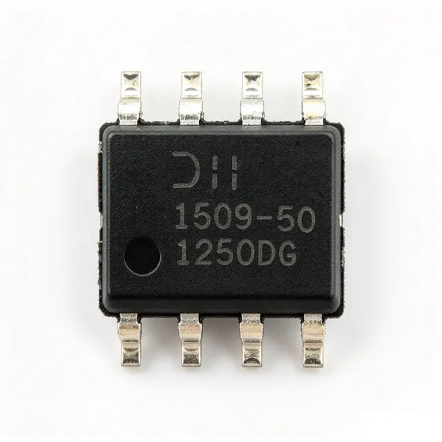
AP1509-50SG-13 - 2A, 150kHz, Fixed 5V Buck Converter | Diodes Inc.
The Diodes Incorporated AP1509-50SG-13 is a monolithic 150 kHz PWM step-down (buck) DC-DC converter in an 8-pin SOIC (SG) package with a fixed 5.0 V output and a 2 A continuous load capability from a 4.5 V to 22 V input rail. Designed as a one-chip switching regulator, it integrates the power switch, oscillator, feedback loop and protection blocks, eliminating the need for an external MOSFET and shrinking the total solution footprint for distributed 5 V point-of-load designs. A buck (step-down) DC-DC converter is a switching voltage regulator that uses an inductor-capacitor energy transfer network to convert a higher DC input into a lower, regulated DC output. Buck regulators deliver far higher efficiency (typically 80-95%) than linear regulators when the input-to-output voltage drop is large, which makes them the preferred topology for stepping down 12 V or 15 V bus rails to logic-level supplies such as 5 V, 3.3 V or 1.8 V. The AP1509-50SG-13 sits in the broader hierarchy of switching regulator -> DC-DC converter -> voltage regulator -> power management IC. Key specifications include a fixed 5 V output, 150 kHz nominal switching frequency, 2 A continuous output current, 4.5 V to 22 V input voltage range, internal MOSFET switch, and built-in thermal shutdown. The 150 kHz switching frequency allows the use of small, low-cost inductors and filter capacitors, while the SOIC-8 footprint offers the same land pattern as the popular LM2596-style 5-pin regulators with a few unused pins. This pin/effort savings is one of the device's primary value propositions. Typical applications include 12 V-to-5 V distributed power buses in consumer electronics, point-of-load regulation after a front-end AC-DC or 24 V industrial supply, battery charger auxiliaries, hobby robotics and Arduino-style 5 V rails, and any cost-sensitive board that previously used an LM7805 linear regulator and now needs higher efficiency. Designers moving from a 7805 typically see efficiency jump from ~40% to ~85% while reducing or eliminating heatsinking. When designing with this part, observe the minimum 4.5 V input headroom and choose an inductor sized for the 2 A saturation rating with low DCR for best efficiency. The AP1509 uses voltage-mode control; for noise-sensitive analog loads a small LC output filter or post-LDO can be added because the ripple at 150 kHz is typically 30-50 mV pk-pk.

AP1661AP-G1 BCM PFC Controller | Diodes Incorporated
The Diodes Incorporated AP1661AP-G1 is a boundary-conduction-mode power-factor-correction controller packaged as an 8-pin PDIP. The device is designed for high-performance PFC power conversion and uses BCM operation to support power-factor correction in switch-mode power supplies. The verified distributor data identifies a 14.5 V supply value, 50 uA startup current, and an operating temperature range of -40°C to 85°C. The AP1661AP-G1 is listed as obsolete in comparison data, so lifecycle planning should confirm availability before committing to new production. A power-factor-correction controller is a power-management semiconductor used in AC-to-DC converters and switch-mode power supplies. Its role is to shape input current so that it is drawn in phase with the AC input voltage, improving true power factor and reducing reactive current. In the broader hierarchy, this part belongs to the PFC-controller class within power-management ICs, alongside voltage regulators, DC-DC converters, supervisors, and motor-driver products. Boundary-conduction-mode control reduces conduction losses by allowing the switching device to conduct near the voltage peak and limiting high-frequency switching activity. The AP1661AP-G1 includes the key verified attributes of BCM PFC operation, an 8-pin PDIP package, through-hole mounting, a 14.5 V supply value, and a 50 uA startup current. Its operating-temperature range is specified as -40°C to 85°C. These values make it relevant to designers evaluating compact, offline power-conversion equipment, especially where a through-hole controller package and established BCM control method are preferred. The package is listed as 8-DIP with a 0.300-inch, 7.62 mm lead pitch in the comparison data. AP1661AP-G1 is commonly associated with PFC stages in offline power supplies, industrial AC-DC converters, appliance power systems, and other mains-powered equipment. The controller coordinates the switching behavior of an external power stage rather than directly regulating an output voltage alone. External magnetics, switching devices, sensing networks, and safety circuitry remain necessary to complete a practical PFC design. Component selection should therefore include validation of switching frequency, current sensing, protection thresholds, startup behavior, and thermal conditions from the manufacturer datasheet. For hardware design, use the manufacturer datasheet and application guidance to select the gate-drive network, current-sense resistor, compensation components, input bridge, output capacitor, boost inductor, and EMI filtering. Keep the high-current switching loop compact and keep sensitive feedback and current-sense traces away from power-node transitions. Because the verified data marks the part obsolete, new designs should confirm lifecycle status, stock, and approved sourcing before layout release. This product page consolidates the verified distributor identity, BCM PFC classification, package information, lifecycle observations, and engineering application guidance for AP1661AP-G1. It distinguishes confirmed values from unavailable specifications and avoids treating similar AP1661 variants as drop-in replacements without explicit evidence.
AP1661MTR-E1 - 0.8A PFC Controller | Diodes Incorporated
The Diodes Incorporated AP1661MTR-E1 is a boundary-conduction-mode power-factor-correction controller with a listed 14.5 V input and 0.8 A output rating, packaged in an 8-pin SOIC. It is designed primarily as the active controller for a boost pre-converter in AC power supplies, where it helps shape input current and reduce reactive power. The verified data identifies the device as an active PFC controller, with an operating temperature range of -40 °C to +85 °C. A power-factor-correction controller is a power-management semiconductor that controls the charging of an energy-storage inductor in an AC-input boost stage. By commanding the switching device according to a suitable conduction method, the controller helps the upstream rectifier draw current near the input-voltage waveform instead of narrow, highly reactive pulses. The result is improved input power factor and lower line-current distortion when paired with the correct power stage and compensation network. The AP1661MTR-E1 uses boundary-conduction mode, identified in the distributor data as BCM. This mode is associated with a boost PFC stage and can simplify control compared with continuous-conduction implementations when the surrounding inductor, switching element, sensing network, and compensation are designed for the intended line input. The verified listing also specifies an SOIC-8 package and a RoHS-compliant part. The listed 0.8 A output and 14.5 V input values should be treated as the available verified parameters, not as a complete electrical rating set. The manufacturer datasheet is required for pin names, thresholds, gate-drive limits, compensation details, start-up behavior, and absolute maximum ratings. AP1661MTR-E1 is marketed as an active component in the retrieved data, while procurement availability and pricing vary by distributor. Typical applications include front-end PFC for industrial power supplies, server and telecom power systems, and AC-DC converters that require reduced input-current distortion. In each case, the controller is only one part of the solution; the boost inductor, switching transistor, rectifier bridge, capacitors, current-sense network, and feedback loop determine the achieved power factor and efficiency. A critical design consideration is validating the complete PFC loop against the minimum and maximum input line, output voltage, load, and switching frequency. Do not infer pin functions, protection behavior, or maximum output power from the distributor summaries alone. Use the manufacturer datasheet and validate startup, overvoltage, overcurrent, zero-cross behavior, and thermal conditions in the target enclosure.
AP1661MTR-G1 - 800mA PFC Controller | Diodes Incorporated
The Diodes Incorporated AP1661MTR-G1 is an active boost power-factor-correction controller rated for 0.800 A output and a 14.5 V VIN condition, supplied in an 8-pin SOIC package. The component is intended primarily as a pre-converter in electronic power supplies where correcting input-current phase and improving power factor are priorities. Its boundary-conduction-mode operation, 600 mA to 800 mA current-related ratings, and 2.5 V reference-related information identify it as a compact PFC solution rather than a conventional standalone regulator. A power-factor-correction controller is an integrated circuit that controls the switching stage of a boost converter so the input current tracks the input voltage more closely than a simple linear or rectifier circuit. In the power-management hierarchy, AP1661MTR-G1 belongs to the PFC controller class, supports a boost-converter topology, and is intended to reduce input-current distortion in AC-to-DC power supplies. Its 8-pin SOIC package is surface-mount compatible and suitable for compact power-conversion boards. Verified distributor information identifies AP1661MTR-G1 as an active, RoHS-compliant SOIC-8 device. The listed operating-temperature range is -40 °C to +85 °C. The available technical summary also reports an 800 mA IOUT condition, a 14.5 V VIN condition, boundary-conduction-mode PFC operation, 600 mA and 800 mA current ratings, a 50 µA current-related specification, and a 2.5 V reference-related specification. Other detailed electrical limits, switching frequency, protection thresholds, pin functions, and timing values are not supplied in the verified data and require the manufacturer datasheet. Typical applications include AC-to-DC front ends for industrial power supplies, server or telecom power-supply modules, adapters, chargers, and other systems where near-unity power factor can reduce reactive and harmonic current. In a practical implementation, the controller drives external MOSFETs, rectifiers, inductors, sensing resistors, and protection circuitry; it does not directly provide the final isolated output voltage. The primary design consideration is ensuring adequate voltage headroom, current sensing, switching-node layout, and thermal capacity for the external boost components. Designers should verify the exact AP1661MTR-G1 datasheet and application circuit before finalizing component values, since the supplied web data does not expose a complete pinout or full timing and electrical tables. This page consolidates verified distributor specifications, package and lifecycle information, replacement-search results, and practical design guidance for engineers evaluating AP1661MTR-G1 in power-factor-correction systems.
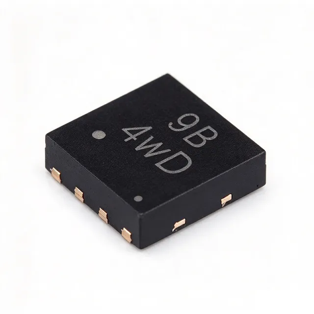
AP3441SHE-7B - 3A, 1MHz Sync Step-Down DC-DC Converter | Diodes
The Diodes Incorporated AP3441SHE-7B is a 3A synchronous step-down (buck) DC-DC converter with a fixed 1 MHz switching frequency and a wide 2.7 V to 5.5 V input range, housed in an 8-pin U-DFN2020-8 (UDFN-8) exposed-pad package. Per the manufacturer datasheet, the device delivers an adjustable output from 0.6 V up to VIN with ±1.5% reference accuracy and supports 100% duty-cycle operation for low-dropout conditions. The synchronous rectifier is integrated on-chip, eliminating the need for an external Schottky diode and simplifying the bill of materials. A buck (step-down) DC-DC converter is a switching regulator that efficiently reduces a higher DC input voltage to a lower DC output voltage by alternately storing energy in an inductor and releasing it into a load. Synchronous buck ICs integrate both the high-side and low-side MOSFETs, replacing the traditional rectifier diode with a low-Rds(on) MOSFET to achieve peak efficiencies above 90%. Within the broader taxonomy, AP3441 belongs to: switching regulator -> DC-DC converter -> power management IC -> semiconductor. It is purpose-built for low-voltage, high-current point-of-load (POL) conversion in portable and space-constrained products. Key features of the AP3441SHE-7B include 55 µA typical no-load quiescent current, sub-1 µA shutdown current, internal soft-start, thermal shutdown, cycle-by-cycle current limit, and constant-frequency PWM control with no required external compensation components. The high 1 MHz switching frequency enables the use of small inductors and ceramic output capacitors, shrinking the total solution footprint to roughly the size of the IC package itself. At heavy loads, the PWM control provides excellent stability and fast transient recovery; at light loads the device automatically transitions to a pulse-frequency modulation (PFM) mode to sustain high efficiency. The architecture uses a peak-current-mode control loop with internal slope compensation and an integrated synchronous MOSFET, allowing stable operation with ceramic output capacitors without ESR-related stability concerns. The exposed thermal pad on the underside of the UDFN-8 package provides a low thermal resistance path to PCB copper, sustaining the 3 A continuous output rating across the -40 °C to +85 °C operating range. Typical applications include single-cell Li+/Li-polymer battery powered systems, USB-powered devices, solid-state drives (SSD), portable media players, point-of-load conversion for FPGAs, ASICs, and DSPs, and distributed 3.3 V/5 V bus regulation in networking and consumer products. The wide input range also makes it suitable for multi-cell alkaline or NiMH battery stacks as well as standard 3.3 V and 5 V rails. When designing, select a 1 µH to 4.7 µH shielded inductor with a saturation rating above the peak inductor current (around 4 A for 3 A loads), place input/output ceramic capacitors as close as possible to the IC, and provide at least four thermal vias under the exposed pad to spread heat. To preserve efficiency, route the feedback trace away from the inductor and switching nodes. This page consolidates tier pricing, drop-in alternatives, and design notes that go beyond the datasheet to accelerate your design-in. This page synthesizes distributor tier pricing, drop-in pin-compatible alternatives, and practical PCB-layout design notes not found in the manufacturer datasheet.

AP61102Z6-7 - 1A Synchronous Buck Converter, 2.3-5.5V | Diodes
The Diodes Incorporated AP61102Z6-7 is a 1 A synchronous step-down (buck) DC-DC converter with a wide 2.3 V to 5.5 V input range and an adjustable output from 0.6 V up to 3.6 V, housed in a compact 6-pin SOT-563 / SOT-666 surface-mount package. The device integrates a 110 mΩ high-side MOSFET and an 80 mΩ low-side MOSFET, providing high-efficiency step-down conversion from common 3.3 V or 5 V supply rails to point-of-load voltages used by SoCs, MCUs, and FPGAs. A buck converter (step-down switching regulator) is a type of DC-DC converter that uses a controlled switch, an inductor, and output capacitance to deliver a lower DC voltage from a higher DC input with high efficiency. Synchronous buck converters replace the conventional Schottky rectifier with a low-side MOSFET, reducing conduction loss and improving thermal performance at moderate-to-high load currents. The AP61102 belongs to the broader hierarchy of DC-DC converters -> switching regulators -> power management ICs, sitting alongside LDOs and charge pumps in modern POL architectures. Key features include a fixed 2.2 MHz switching frequency that allows the use of small inductors and ceramic output capacitors, a Constant On-Time (COT) control architecture that delivers fast transient response, low quiescent current suitable for always-on and partial-power applications, internal soft-start, Power-Good (PG) indication, and full protection with over-current, over-voltage, short-circuit, and thermal shutdown. The 2.2 MHz switching frequency stays above the AM broadcast band, simplifying EMI filtering. The AP61102 uses Diodes' proprietary COT control topology, which eliminates the need for an external compensation network. Compared with traditional voltage-mode or current-mode buck regulators, COT delivers faster transient response to load steps and simpler external BOM with typically only an inductor and two ceramic capacitors required. Typical applications include USB Type-C / 5 V-powered IoT nodes, solid-state drives and storage modules, single-cell Li-ion battery-powered portable electronics, home automation gateways, 3.3 V POL rails for low-power MCUs, and wearables that need a small footprint and high efficiency across light and heavy loads. When designing, keep the input capacitor within 2 mm of the VIN and PGND pins to suppress switching noise, select a 1 µH to 2.2 µH shielded inductor with low DCR for best efficiency, and reserve PG for sequencing or fault monitoring in multi-rail systems. The 6-pin SOT-563 footprint is among the smallest 1 A buck footprints available. This page combines verified distributor pricing, drop-in same-package alternatives, and practical PCB design notes not consolidated in the manufacturer datasheet, giving engineers a single reference for sourcing and second-source decisions.
AP62200TWU-7 - 18V/2A Sync Buck Converter, TSOT-23-6 | Diodes Inc
The Diodes Incorporated AP62200TWU-7 is a 2A synchronous step-down buck converter accepting a wide 4.2V to 18V input range and producing an adjustable 0.8V to 7V output, housed in a 6-pin TSOT-23-6 (TSOT26) package. It integrates a 90mΩ high-side MOSFET and a 65mΩ low-side MOSFET, achieving high-efficiency DC-DC conversion at 750kHz switching frequency with PFM light-load operation. According to the Diodes AP62200 datasheet, this device targets compact point-of-load applications where small PCB footprint and high efficiency are required. A buck converter (step-down switching regulator) is a type of DC-DC converter that uses an internal high-side switch, an external inductor, and synchronous rectification to produce an output voltage lower than its input. It belongs to the switching regulator family within the power management IC hierarchy: buck converter -> switching regulator -> DC-DC converter -> power management IC -> semiconductor. Synchronous buck converters replace the external Schottky diode with an internal low-side MOSFET, dramatically improving efficiency at light loads and shrinking the solution footprint. Key features include 4.2V to 18V wide input range, 2A continuous output current, 0.8V to 7V adjustable output via external resistor divider, 750kHz switching frequency with PFM pulse-skipping at light loads, internal 90mΩ/65mΩ power MOSFETs, and built-in protection including over-current protection (OCP), over-temperature protection (OTP), and under-voltage lockout (UVLO). The TSOT-23-6 package enables designs as small as a few external passive components. The AP62200TWU-7 uses constant-on-time (COT) control architecture, providing fast transient response and simple loop compensation. Compared to traditional voltage-mode or current-mode buck converters, COT architecture requires no external compensation network, reducing BOM cost and PCB area. The integrated synchronous MOSFETs eliminate the need for an external Schottky diode, further simplifying the design and improving efficiency to peak values typically above 90% at moderate loads. Typical applications include distributed 5V/3.3V/1.8V/1.2V rails in set-top boxes, networking equipment, surveillance cameras, IoT gateways, LCD displays, and consumer electronics. The wide 4.2V to 18V input range makes the AP62200TWU-7 suitable for both 5V USB-powered systems and 12V industrial bus systems. When designing with this device, ensure the input capacitor (typically 22µF ceramic) is placed close to the IC pins and the feedback resistor divider uses 1% tolerance resistors for accurate output voltage regulation.