Товары (38.000+)

S912ZVL64F0MLF - S12Z MagniV 64KB Flash 32MHz Auto MCU | NXP
S912ZVL64F0MLF

S912ZVL64F0MLF - S12Z MagniV 64KB Flash 32MHz Auto MCU | NXP

The NXP Semiconductors S912ZVL64F0MLF is an automotive-qualified 16-bit microcontroller based on the S12Z CPU core, delivering 64KB of on-chip Flash, 32 MHz CPU clock, and integrated analog peripherals in a 48-pin LQFP (7x7 mm) package with -40C to +125C operating range. The MagniV family combines the S12Z core with a high-voltage analog front end and LIN/CAN connectivity, targeting body and chassis applications where reducing PCB area and BOM count is critical. The part operates from a 3.3 V or 5 V supply and is qualified to automotive standards, allowing direct deployment under the hood, in DC motor control, or in sensor interface modules. A microcontroller (MCU) is a single-chip computer that integrates a CPU core, program and data memory, peripheral interfaces, and analog/digital I/O. The S12Z belongs to the 16-bit CISC family originally derived from the Freescale HC12/S12 architecture, modernized to deliver higher code density, faster context switching, and improved peripheral integration. Within the broader semiconductor taxonomy, the S12Z MCU sits inside the automotive-qualified microcontroller segment, between the 8-bit S08 family (lower cost) and the 32-bit Kinetis/S32K families (higher performance). The MagniV line further embeds high-voltage analog blocks, enabling direct connection to 12 V automotive buses without external drivers. Key features of the S912ZVL64F0MLF include 64KB Flash, 4KB RAM, an integrated 12-bit ADC, PWM channels, timers, GPIO, SCI/SPI/IIC communication peripherals, and a CAN 2.0 module. The 48-LQFP package exposes ample I/O while fitting compact body-electronics PCBs. The wide -40C to +125C automotive temperature grade makes the device suitable for under-hood and chassis environments that experience large thermal swings. Internal voltage regulation and an on-chip debug (BDM) interface simplify in-circuit programming and field firmware updates. Typical applications include automotive body control modules, HVAC blower controls, window lift and door modules, lighting controllers, dashboard clusters, and small sensor nodes that require CAN or LIN connectivity. The integrated analog front end is particularly useful for brush-DC motor control, solenoid drive, and switch-contact debouncing, replacing discrete driver ICs. Designers should evaluate the analog channel count and high-voltage tolerance relative to system needs. The 48-LQFP footprint, automotive qualification, and balanced peripheral set make S912ZVL64F0MLF a strong fit when BOM consolidation outweighs the need for 32-bit performance. This page consolidates distributor pricing, drop-in same-family alternatives, and practical design notes for engineers evaluating the S912ZVL64F0MLF for automotive body electronics.

Запрос цены Контакты
S912ZVL64F0VLC - 64KB Flash S12Z MagniV MCU | NXP | Automotive
S912ZVL64F0VLC

S912ZVL64F0VLC - 64KB Flash S12Z MagniV MCU | NXP | Automotive

The NXP S912ZVL64F0VLC is a 16-bit S12Z MagniV mixed-signal microcontroller built on a 0.18 µm automotive-qualified process, integrating 64KB of Flash, 1KB of EEPROM, 4KB of SRAM, and an analog front end in a 32-pin LQFP package measuring 7 mm x 7 mm with 0.8 mm pitch. It runs at up to 32 MHz, supports 3.3 V and 5 V supply rails across an extended automotive voltage range up to 18 V, and is qualified to AEC-Q100 Grade 1 (-40 °C to +125 °C) for body and chassis ECUs. A microcontroller (MCU) is a single-chip processor that integrates a CPU core, non-volatile program memory, working RAM, and a configurable set of analog and digital peripherals. The S12Z family is NXP's 16-bit CISC architecture, derived from the long-lived HC12/S12X lineage, paired here with NXP's MagniV single-chip integration concept in which a high-voltage analog front end and a microcontroller die share one package. The 'V' family segment targets 12 V automotive body and chassis applications where the MCU can directly sense and drive 12 V loads and survive load-dump transients up to 18 V. Key features include an integrated 12 V analog front end (LIN, GPIOs with high-V tolerance, a 12-bit ADC and timers), a BDM (background debug mode) interface for non-intrusive programming, an on-chip voltage regulator, and built-in safety support such as a window watchdog and a power-on reset. The device targets LIN-slave body controllers and mechatronic sub-modules where board area is at a premium and external high-side drivers and regulators are undesirable. The S12Z core is a pipelined 16-bit CISC engine whose instruction set is forward-compatible with legacy HC12/S12 code, and the part uses a uniform 64 KByte Flash array with ECC, plus EEPROM for small parameter storage. Peripherals are arranged through NXP's standard S12Z Global Express Map and can be relocated, which simplifies software partitioning across multiple addresses. Typical applications include automotive body controllers (BCM, door modules, mirror control), HVAC actuators and small motor drivers, and HVAC/lighting switch interfaces. Choose this part when you need a 32 MHz 16-bit core with 64 KB Flash at 32-LQFP and AEC-Q100 Grade 1 qualification, with the analog front end capable of handling 12 V directly. When designing with this device, ensure the decoupling network uses at least two capacitors per supply pin (one bulk plus one 100 nF) and that the high-voltage analog pins adhere to NXP's ESD-robust PCB layout rules. This page synthesizes distributor pricing, automotive-grade alternatives, and practical design notes not found in the manufacturer datasheet.

Запрос цены Контакты
S912ZVLA12F0MLC - S12Z 128KB Flash MagniV MCU | NXP | Automotive LIN
S912ZVLA12F0MLC

S912ZVLA12F0MLC - S12Z 128KB Flash MagniV MCU | NXP | Automotive LIN

The NXP S912ZVLA12F0MLC is a 16-bit S12Z MagniV mixed-signal microcontroller from the S12ZVL platform, featuring 128KB of Flash memory, a 32MHz S12Z core, and an integrated 12V-to-5V voltage regulator with LIN physical-layer transceiver in a 32-pin LQFP (7x7 mm) package. It is automotive-qualified to -40°C to +125°C and targets space-constrained automotive LIN nodes where on-board power conversion and bus connectivity must coexist with application logic on a single die. What is a MagniV mixed-signal MCU? The MagniV family from NXP combines an S12/S12Z microcontroller core with high-voltage analog and LIN/CAN physical-layer peripherals in a single IC. In the system hierarchy this part sits at: microcontroller (MCU) -> mixed-signal MCU -> automotive microcontroller -> embedded controller. MagniV parts are designed to reduce external components in body-electronics and sensor-node designs by absorbing the 12V LDO and the LIN transceiver into the MCU. Key features include 128KB Flash (128K x 8), 32MHz S12Z CPU core with CISC instruction set, on-chip 12V-to-5V regulator, integrated LIN transceiver, 10-bit ADC, automotive temperature grade (-40°C to +125°C), and a 32-pin LQFP package. The integrated voltage regulator accepts direct 12V automotive battery input and supplies the internal 5V logic, eliminating the need for an external LDO in the typical LIN sensor node. Technical depth: the S12Z core is an enhanced 16-bit CISC architecture with improved addressing, hardware multiply/divide, and a more efficient instruction pipeline than legacy HC12/S12X cores. The integrated LIN transceiver is compliant with LIN 2.x/ISO 17987 physical-layer specifications, allowing the part to communicate directly on the LIN bus with no external transceiver IC. On-chip peripherals (timers, PWM, SCI, SPI) provide the typical motor/sensor control capability required for body-electronics modules. Typical applications include automotive LIN sensor nodes (seat occupancy, rain/light, HVAC flap), body controllers, simple motor controllers, and 12V-powered smart actuators. The S12ZVL's integrated 12V LDO + LIN transceiver make it especially well suited to cost-sensitive body-electronics nodes where PCB area and BOM count are critical. When designing with this device, verify the integrated 12V-to-5V regulator's thermal dissipation budget at full LIN current. The LQFP-32 (7x7) package has limited theta_JA headroom; at 12V input and 50mA load the part dissipates ~350mW, which is acceptable without a heatsink, but higher load currents demand thermal verification. This page synthesizes distributor pricing, same-package alternatives from the S12ZVL family, and practical design notes not found in the manufacturer datasheet alone.

Запрос цены Контакты
S912ZVLA64F0MLF - S12Z MagniV 64KB Flash 32MHz MCU | NXP
S912ZVLA64F0MLF

S912ZVLA64F0MLF - S12Z MagniV 64KB Flash 32MHz MCU | NXP

The NXP Semiconductors S912ZVLA64F0MLF is a 16-bit automotive microcontroller from the S12 MagniV mixed-signal MCU family, featuring an S12Z core running at 32 MHz with 64 KB of on-chip Flash memory in a 48-pin LQFP (7x7 mm) package. It is automotive-qualified (AEC-Q100) and operates across a -40C to +125C temperature range, targeting space-constrained automotive LIN nodes. The integrated peripherals include a 12V-to-5V voltage regulator and a LIN physical-layer transceiver that consolidate what would otherwise require multiple external ICs. An automotive LIN microcontroller is a mixed-signal MCU purpose-built for Local Interconnect Network (LIN) nodes in vehicle body electronics. The LIN bus is a low-cost single-wire serial protocol standardized under ISO 17987, widely used for non-critical body and comfort subsystems (window lifters, mirror adjusters, seat controllers, HVAC dampers). At a higher level, this part belongs to the hierarchy: automotive MCU -> mixed-signal MCU -> 16-bit MCU -> S12 MagniV family -> NXP semiconductor IC. By integrating the LIN transceiver and a 12V-tolerant regulator on-die, the S12ZVL family eliminates the need for external bus-driver ICs and reduces BOM cost on the smallest LIN slaves. Key features include 64 KB Flash, 32 MHz S12Z CPU core, 1 KB EEPROM, 4 KB RAM, integrated LIN 2.x/SAE J2602 transceiver with bus-pin protection, integrated 5V LDO regulator accepting 6V to 18V supply, and on-chip CAN (msCAN) and SPI/SCI peripherals. The 48-LQFP-7x7 footprint is shared across the S12ZVL sub-family, enabling drop-in scalability between 8 KB, 16 KB, 32 KB, 64 KB, and 128 KB Flash options. The S12Z core uses a 32-bit instruction path with 16-bit arithmetic to optimize code density and execution speed for byte-oriented automotive software stacks, while keeping the addressable memory model compatible with the earlier S12 architecture. The integrated Vreg and LIN phy reduce PCB area and EMI compared to multi-chip LIN slave implementations. Typical applications include automotive body control modules such as window lifters, seat controllers, HVAC damper actuators, mirror adjusters, sunroof controllers, ambient lighting LED drivers, and simple sensor interfaces that communicate over LIN back to a central body controller. The AEC-Q100 Grade 0 qualification and 12V battery-direct tolerance make it well suited for connection directly to the automotive 12V bus. When designing with this part, ensure the LIN bus load and termination meet SAE J2602 specifications, and verify that the supply decoupling handles cranking transients (ISO 7637-2 pulses). The integrated Vreg caps the dissipation envelope, but PCB copper area should still be sized for sustained wake-up currents. This page synthesizes authorized distributor pricing, drop-in S12ZVL family alternatives, and practical PCB-decoupling notes not found on the manufacturer product page alone.

Запрос цены Контакты
S912ZVMC12F1MKH - S12Z MagniV 16-bit MCU, 128KB Flash | NXP
S912ZVMC12F1MKH

S912ZVMC12F1MKH - S12Z MagniV 16-bit MCU, 128KB Flash | NXP

The NXP S912ZVMC12F1MKH is a 16-bit S12Z MagniV microcontroller featuring 128 KB of embedded Flash, an integrated 12V analog supply regulator, and a high-speed analog front-end, all housed in a 64-pin HLQFP (10x10) package with automotive-grade qualification. The device operates at a 50 MHz internal bus clock, integrates 2 KB of SRAM and 1 KB of EEPROM, and is targeted at motor control and DC-DC power conversion applications. As a member of the S12Z MagniV family, this device belongs to the broader category of 16-bit microcontrollers (MCU), a class of embedded processors offering an efficient balance between deterministic performance, code density, and peripheral integration. S12Z cores extend the legacy HC(S)12 instruction set with up to 32-bit wide operations and a dedicated memory management unit, serving as a bridge between classic 8/16-bit designs and 32-bit Cortex-M parts while remaining automotive-qualified by default. Key features include an integrated 12V-to-5V analog supply regulator eliminating external power management ICs, a built-in CAN (MSCAN) and LIN (SCI) interface for in-vehicle networking, a 12-bit ADC with internal 5V reference, and an enhanced capture timer / PWM module suitable for three-phase motor commutation. The 64-pin HLQFP-EP package adds an exposed thermal pad (theta_JA around 35 C/W) for high-current driver stages. The architecture pairs the S12Z CPU with crossbar-based peripheral routing and a unified memory map, allowing deterministic interrupt response without external bus arbitration. Hardware emulation and on-chip trace support are available through NXP's BDM and background debug interfaces, while industrial application needs are met via ECC on Flash and SRAM. Typical applications include 12V automotive fuel pumps, HVAC blowers, BLDC/PMSM motor drives (under 1 kW), DC-DC converter control, and body electronics modules. The integrated 12V regulator allows direct connection to the automotive battery rail. When laying out this part, provide a generous copper land under the exposed pad and at least four thermal vias to the inner PCB plane to keep junction temperature within rated limits during continuous motor-drive load. Decouple the integrated 5V regulator and the core supply pins separately with 100 nF plus 4.7 µF capacitors as shown in the NXP reference design. This page consolidates distributor pricing, drop-in NXP S12Z alternatives, and practical design notes that go beyond the manufacturer datasheet to help engineers select, source, and integrate the S912ZVMC12F1MKH.

Запрос цены Контакты
S912ZVMC12F3WKH - MagniV 16-bit S12Z MCU, 128KB Flash | NXP
S912ZVMC12F3WKH

S912ZVMC12F3WKH - MagniV 16-bit S12Z MCU, 128KB Flash | NXP

The NXP S912ZVMC12F3WKH is a 16-bit S12 MagniV mixed-signal microcontroller from the S12ZVM family, integrating 128 KB of Flash memory and running the S12Z CPU core at up to 50 MHz, housed in a 64-pin HLQFP (10x10 mm) package with exposed thermal pad. What is a MagniV mixed-signal microcontroller? A MagniV device is a single-chip automotive MCU that combines the S12/S12Z CPU core with high-voltage analog peripherals - most importantly an on-chip 12 V to 5 V voltage regulator and a LIN physical layer. Within the broader taxonomy, S12ZVM sits as: 16-bit MCU -> automotive microcontroller -> mixed-signal MCU -> embedded controller -> semiconductor. The "MagniV" branding means the part is intended for direct connection to a 12 V automotive bus without an external 5V regulator, dramatically shrinking the BOM for body and motor-control ECUs. Key features of the S912ZVMC12F3WKH include 128 KB (128K x 8) of Flash program memory, an integrated 12 V to 5 V LDO for direct automotive battery operation, a LIN physical interface for in-vehicle networking, and a -40C to +150C operating temperature range (AEC-Q100 automotive grade). The device integrates gated timer units (GTM/ECT) suitable for 3-phase motor control, plus ADC, PWM, and an enhanced capture timer. Architecturally, the S12ZVM combines a CISC S12Z CPU with the high-voltage analog front end described in the NXP reference manual. The on-chip regulator eliminates the external 12V-to-5V buck or LDO that typical 5V microcontrollers still require, reducing PCB area by up to 30 percent in sensored BLDC/PMSM/sensorless motor designs. Typical applications include 3-phase brushless DC (BLDC) motor control for automotive auxiliary pumps and fans, permanent magnet synchronous motor (PMSM) drives, switched reluctance motor (SRM) control, body electronics modules with LIN connectivity, and industrial motor-control platforms up to 12V supply. When designing with this part, carefully observe the high-voltage analog layout guidelines in the S12ZVM reference manual: keep the exposed pad soldered to a copper pour, route the LIN bus traces with controlled impedance, and place the 12V bulk capacitor as close to the HV supply pin as possible to handle load-dump transients. This page synthesizes distributor pricing, drop-in same-package S12ZVM and S12ZVC family alternatives, and practical high-voltage mixed-signal design notes that complement (not duplicate) the manufacturer datasheet.

Запрос цены Контакты
S912ZVMC64F3MKH - S12Z 50MHz 64KB Flash MCU | NXP MagniV
S912ZVMC64F3MKH

S912ZVMC64F3MKH - S12Z 50MHz 64KB Flash MCU | NXP MagniV

The NXP Semiconductors S912ZVMC64F3MKH is a 16-bit S12Z MagniV microcontroller featuring a 50MHz S12Z core, 64KB Flash, 4KB RAM, and integrated CANbus/SCI/SPI connectivity, housed in a 64-pin HLQFP (10x10 mm) package with exposed thermal pad. Designed for space-constrained automotive body and chassis applications, the S12 MagniV family integrates the S12Z CPU core together with high-voltage analog and CAN physical interface blocks on a single die, eliminating external transceiver and voltage-regulator components. A microcontroller (MCU) is a single-chip computer containing a CPU core, non-volatile program memory (Flash), working memory (RAM), and a configurable set of peripherals such as timers, ADC, communication controllers, and GPIO. Within the broader semiconductor taxonomy, an MCU belongs to the logic IC family, then to the embedded processor hierarchy, then to the automotive-qualified sub-class when AEC-Q100 qualification applies. The S12 MagniV line is purpose-built for the in-vehicle networking segment where single-chip integration reduces PCB area, BOM count, and bill-of-materials cost compared with a discrete MCU plus external LIN/CAN transceiver approach. Key features of the S912ZVMC64F3MKH include 64KB on-chip Flash (64K x 8), 4KB RAM, 512 bytes EEPROM, 31 GPIO, a 10-channel PWM module, DMA, watchdog, and power-on reset. The integrated CANbus controller supports both standard and extended frame formats and is widely used in automotive body control modules such as HVAC, lighting, and door/window controllers. Operating temperature spans -40C to +125C, qualifying the device for AEC-Q100 Grade 1 automotive environments. Architecturally the device pairs the S12Z CPU (an enhanced 16-bit core with improved instruction throughput over the legacy S12X) with on-chip voltage regulator and CAN PHY, enabling direct 12V battery connection with minimum external components. The single-die integration reduces quiescent current paths and improves electromagnetic compatibility versus discrete solutions. Typical applications include automotive HVAC control modules, body controllers, door modules, seat controllers, lighting controllers, and small DC motor control nodes where the CAN interface, small footprint, and integrated high-voltage tolerance simplify design. The exposed pad on the LQFP-64 package provides a low thermal resistance path for sustained processor activity. Designers should note that the -40C to +125C operating range supports under-hood and cabin mounting, while the integrated 5V regulator powers both the internal logic and external sensors. Proper decoupling of the high-voltage analog supply (VDDX) and the digital logic supply (VDDR) is essential for clean CAN signaling. This page synthesizes distributor pricing, drop-in alternatives, and practical design notes not found in the manufacturer datasheet.

Запрос цены Контакты
S912ZVMC64F3VKH - S12Z 16-bit MCU, 64KB Flash, CAN, 64-LQFP | NXP
S912ZVMC64F3VKH

S912ZVMC64F3VKH - S12Z 16-bit MCU, 64KB Flash, CAN, 64-LQFP | NXP

The NXP Semiconductors S912ZVMC64F3VKH is a 16-bit microcontroller from the S12 MagniV family, built around the S12Z CPU core, integrating 64KB of Flash program memory and a CAN controller, packaged in a 64-pin LQFP (10x10 mm). It operates at up to 50 MHz core clock, offers 31 general-purpose I/O pins, and targets automotive and industrial real-time control applications where integration, deterministic interrupt response, and on-chip analog are valued. A microcontroller (MCU) is a single-chip computer that integrates a CPU, memory (Flash/RAM), and a rich set of peripherals such as timers, ADCs, communication controllers, and GPIO into one package. MCUs span the hierarchy: microcontroller -> embedded processor -> semiconductor device. The S12Z core is a 16-bit enhanced superset of the long-running Freescale/NXP S12 architecture, optimized for high code density, fast context switching, and 32-bit-aware instruction extensions while preserving the S12 ecosystem. Key features of the S912ZVMC64F3VKH include 64KB Flash with 512 bytes EEPROM and 4KB RAM (per the verified vendor description), a CAN 2.0 interface alongside SCI and SPI connectivity, DMA channels, a programmable watchdog timer (WDT), power-on reset (POR), and PWM generators suitable for motor and DC/DC control loops. The 64-LQFP package provides an exposed thermal pad that significantly lowers theta-JA versus non-EP variants. Technically, the MagniV integration brings the S12Z core, voltage regulator, and analog front-end together to reduce external component count for sensor-driven and motor-driven ECUs. The 50 MHz core plus enhanced interrupt controller enables deterministic response to time-critical events such as field-oriented control (FOC) loops or CAN message handling. This device family is commonly used where developers need the proven HCS12 toolchain rather than migrating to a Cortex-M0/M0+ device. Typical applications for this MagniV MCU include automotive HVAC and climate control, BLDC/PMSM motor control, body and convenience modules, industrial sensors, and small-signal sensing front-ends. The integrated CAN controller makes it a natural fit for in-vehicle networking nodes communicating on the CAN bus. When designing with this device, ensure the supply decoupling follows NXP's reference board layout, place a 100 nF X7R capacitor adjacent to every supply pin, and bond the exposed pad (EP) to a copper pour of at least 1 square inch to keep junction temperatures inside the automotive-grade envelope. This page synthesizes distributor pricing, same-family NXP drop-in alternatives, and application guidance not assembled on any single manufacturer datasheet sheet.

Запрос цены Контакты
S912ZVML32F1WKH - 50MHz 32KB Automotive 16-Bit MCU | NXP
S912ZVML32F1WKH

S912ZVML32F1WKH - 50MHz 32KB Automotive 16-Bit MCU | NXP

The NXP Semiconductors S912ZVML32F1WKH is an automotive-qualified 16-bit S12Z MagniV microcontroller operating at 50 MHz, with 32 KB of embedded ECC Flash and a 64-pin HLQFP package measuring 10 mm by 10 mm. Its stated -40 °C to +150 °C temperature range supports demanding automotive and industrial environments where extended-temperature operation, mixed-signal control, and deterministic embedded processing are important. A microcontroller is a programmable semiconductor that integrates a processor core, nonvolatile program memory, volatile data memory, peripherals, and communication interfaces on one device. The S12Z belongs to the MagniV mixed-signal family and is positioned below the general MCU hierarchy as a 16-bit embedded controller for real-time motor-control, sensing, and actuator-management systems. This product type combines digital control logic with analog measurement resources needed for closed-loop systems. Verified headline features include an enhanced S12Z core, 50 MHz bus speed, 32 KB Flash organized as 32K by 8 bits, and a -40 °C to +150 °C automotive temperature range. The available family information also identifies ECC-supported Flash, EEPROM, RAM, a six-channel periodic interrupt-function timer, a 15-bit PWM module with dead time and fault management, and dual 12-bit ADCs. These resources support deterministic timing, motor commutation, current sensing, diagnostics, and safety-related control functions. The MagniV architecture targets efficient mixed-signal motor-control applications rather than general-purpose computing. At 50 MHz, the MCU provides substantially more instruction-processing headroom than slower 8- or 16-bit controllers. ECC protection for Flash, EEPROM, and RAM helps detect stored-memory errors, while the extended-temperature grade supports operation beyond conventional commercial conditions. These characteristics make the device relevant to automotive electronics, industrial drives, and equipment requiring robust embedded control. Typical uses include three-phase brushless DC motor control, permanent-magnet synchronous motor control, electric vehicle power electronics, industrial automation, and embedded sensor systems. The PWM dead-time and fault-management functions are especially useful when upper- and lower-side switches must be coordinated safely. Dual 12-bit ADCs can measure analog quantities associated with rotor position, current, voltage, temperature, or protection circuits, subject to application-level design and signal conditioning. The most important layout consideration is the exposed thermal pad and 64-pin QFP footprint. The pad should be connected according to the manufacturer package guidance and tied to the appropriate board plane, with adequate copper to improve heat dissipation. Keep analog inputs, high-current switching nodes, and sensitive sensor traces away from noisy power-stage routes. Firmware, pin multiplexing, electrical limits, decoupling, and timing must be verified against the manufacturer datasheet before production use. This product record combines verified distributor data, family-level technical information, package data, and an explicitly constrained alternative analysis. It distinguishes confirmed values from unavailable details, avoids inventing electrical limits or pin functions, and focuses replacement comparisons on same-footprint NXP candidates whose published S12Z, memory, frequency, and package characteristics can be checked before redesign.

Запрос цены Контакты
S912ZVML64F1MKH557 - MagniV S12Z 64KB 50MHz MCU | NXP
S912ZVML64F1MKH557

S912ZVML64F1MKH557 - MagniV S12Z 64KB 50MHz MCU | NXP

The NXP Semiconductors S912ZVML64F1MKH557 is a 16-bit MagniV S12ZVM mixed-signal microcontroller with an S12Z core running at 50 MHz, 64 KB of on-chip Flash memory, an operating temperature range of -40C to +125C, and automotive qualification, housed in a 64-pin LQFP (10x10 mm) package. A MagniV mixed-signal microcontroller is a single-chip solution that combines a microcontroller core with embedded analog power functions such as voltage regulation and motor-control peripherals. In the power-management hierarchy, the S12ZVM family sits between a standard MCU and a discrete system: it integrates a 12 V to 5 V voltage regulator, LIN/CAN physical connectivity support, and 3-phase motor-control peripherals, replacing an MCU-plus-regulator two-chip solution in automotive and industrial nodes. Key features include the efficient 16-bit S12Z core with 50 MHz bus operation, 64 KB Flash for application code, and integrated analog motor-control resources targeting Brushless DC (BLDC), Permanent Magnet Synchronous Motor (PMSM), and Switched Reluctance Motor (SRM) applications. The automotive temperature grade of -40C to +125C supports under-hood and body electronics environments. Technically, the S12 MagniV S12ZVM family is described by NXP as offering the smallest, efficient, and scalable 3-phase motor control solution. Integration of the 12 V-to-5 V regulator and LIN transceiver support reduces board area, component count, and system cost compared with a discrete MCU plus external regulator and transceiver design. Typical applications include automotive BLDC/PMSM motor drives (pumps, fans, actuators), industrial 3-phase motor control, and LIN/CAN networked body-electronics nodes requiring a single mixed-signal chip. Design consideration: verify the exact device configuration suffix (the 557 ordering code) against the NXP ordering-information table, as Flash size, temperature grade, and package options vary across S912ZVML64 orderable variants. This page synthesizes distributor availability data, same-family drop-in variants, and practical design notes not consolidated in the manufacturer datasheet.

Запрос цены Контакты
S9KEAZ64ACLH - 64KB Cortex-M0+ MCU 48MHz | NXP Kinetis KEA
S9KEAZ64ACLH

S9KEAZ64ACLH - 64KB Cortex-M0+ MCU 48MHz | NXP Kinetis KEA

The NXP Semiconductors S9KEAZ64ACLH is a 32-bit automotive-grade microcontroller based on the ARM Cortex-M0+ core running at up to 48 MHz, with 64 KB of embedded flash memory in a 64-pin LQFP (10x10 mm) surface-mount package. It belongs to the Kinetis KEA (KEA128) sub-family, engineered for cost-sensitive automotive and industrial applications. A microcontroller (MCU) is a single-chip computer that integrates a processor core, program memory, data memory, and peripherals such as timers and communication interfaces. Within the embedded systems hierarchy, the S9KEAZ64ACLH sits in the 32-bit general-purpose MCU class, positioned as a low-cost, high-reliability alternative to 8-bit devices while remaining fully pin- and software-scalable across the KEA family. Key features include the ultra-low-power Cortex-M0+ core, up to 48 MHz operating frequency, 64 KB (64K x 8) flash, connectivity peripherals (CAN, LIN, I2C, SPI, UART/USART), and system peripherals (LVD, POR, PWM, WDT). The KEA family provides robust EMC/ESD performance, high-temperature operation, and low radiated emissions, per NXP product documentation. Technically, the KEA128 sub-family combines an ARM Cortex-M0+ pipeline with automotive-grade qualification, targeting 5V-tolerant I/O designs and motor-control-oriented timers. With 57 GPIO lines, the S9KEAZ64ACLH supports direct drive of relays, LEDs, and motor-control bridges. The CAN and LIN interfaces make it a natural fit for in-vehicle body networks where a single chip must bridge high-speed and low-speed buses. Typical applications include automotive body electronics (window lifters, seat control, lighting modules), brushed and stepper motor control in HVAC actuators, and industrial end nodes requiring CAN connectivity with strict EMC requirements. Design consideration: the Cortex-M0+ lacks hardware divide and DSP instructions compared with Cortex-M4 alternatives, so algorithms requiring heavy arithmetic should be benchmarked, while simple control loops benefit from the deterministic, interrupt-fast design and very low interrupt latency. This page synthesizes distributor pricing, drop-in same-family alternatives, practical design notes, and cross-reference comparison data not found in the manufacturer datasheet.

Запрос цены Контакты
S9KEAZ64AVLK - Kinetis KEA64 32-bit MCU 48MHz 64KB | NXP
S9KEAZ64AVLK

S9KEAZ64AVLK - Kinetis KEA64 32-bit MCU 48MHz 64KB | NXP

The NXP Semiconductors S9KEAZ64AVLK is a Kinetis KEA64 series 32-bit microcontroller based on the Arm Cortex-M0+ core, running at up to 48 MHz with 64 KB of embedded flash memory, housed in an 80-pin LQFP (14 x 14 mm) surface-mount package. According to NXP product data, it belongs to the Kinetis E family targeted at cost-sensitive automotive and industrial applications requiring high quality and long-term longevity support. A microcontroller unit (MCU) is a single integrated circuit that combines a processor core, memory (flash and SRAM), and a rich set of peripherals onto one chip, forming the lowest layer of the embedded-system hierarchy: MCU -> embedded processor -> semiconductor device. The KEA64 sub-family sits within the broader Kinetis EA series, which NXP positions as a scalable, robust performance solution for harsh electromagnetic environments. Key features include the low-power Arm Cortex-M0+ core, 8 KB to 128 KB scalable embedded flash across the sub-family (64 KB on this device), excellent EMC/ESD performance, high-temperature operation, and low radiated emissions - attributes directly cited by NXP for automotive body and motor-control designs. Technically, the Cortex-M0+ pipeline and the KEA family peripheral set (timers, ADC, communication interfaces per the KEA128 sub-family data sheet, document identifier S9KEA128P80M48SF0 as listed in distributor records) deliver deterministic real-time behavior with very low dynamic power. The device operates from a nominal 3.3 V / 5 V supply class per distributor parametric listings, simplifying integration into legacy 5 V automotive modules. Typical applications include automotive body electronics (window lift, door modules), small motor control (BLDC/PMSM), LIN-bus networked sensors, and industrial control nodes where EMC robustness and lifecycle longevity outweigh raw compute performance. Design consideration: confirm the exact supply-voltage class and peripheral configuration against the official KEA128 sub-family data sheet before layout, and reserve flash headroom because the 64 KB density is the mid-point of a sub-family spanning 8 KB to 128 KB. This page synthesizes distributor pricing context, verified drop-in alternatives, practical design notes, and an application-by-application selection guide not found in the manufacturer datasheet, with all parameters traced to cited sources.

Запрос цены Контакты
S9KEAZN8ACFK - KEA 32-bit MCU 48MHz 8KB Flash QFN-24 | NXP
S9KEAZN8ACFK

S9KEAZN8ACFK - KEA 32-bit MCU 48MHz 8KB Flash QFN-24 | NXP

The NXP S9KEAZN8ACFK is an ARM Cortex-M0+ based Kinetis E automotive-qualified 32-bit microcontroller with 48 MHz CPU, 8 KB Flash, and 24-pin QFN (4x4) packaging. The KEA8 sub-family combines a small footprint with automotive-grade temperature and EMC robustness for cost-sensitive embedded control applications. What is a KEA microcontroller? The KEA (Kinetis E Automotive) family is a subset of NXP's Kinetis 32-bit MCU lineup targeting entry-level automotive and industrial applications. In the broader taxonomy, KEA devices are 32-bit microcontrollers within ARM Cortex-M0+ based microcontrollers, themselves a subset of microcontrollers (MCUs), and ultimately embedded computing semiconductors. The 'E' suffix denotes AEC-Q100 Grade 1 automotive qualification, distinguishing KEA parts from general-purpose Cortex-M0+ MCUs. KEA parts share a common SVD/header set and peripheral IP, allowing code portability across KEA sub-families (KEA8, KEA64, KEA128). Key features of the S9KEAZN8ACFK include a Cortex-M0+ core at 48 MHz, 8 KB program Flash, 1 KB SRAM, an 8-channel 12-bit SAR ADC, FlexIO, and multiple communication peripherals (SCI/UART, SPI, I2C). The wide supply range of 2.7 V to 5.5 V supports both 3.3 V and 5 V automotive bus environments. An integrated low-power stop and wait mode with fast wakeup time supports battery-saving requirements. The AEC-Q100 Grade 1 qualification covers -40C to +125C operating temperature. The KEA architecture uses a von Neumann bus matrix, single-cycle GPIO access, and a tightly-coupled peripheral bridge, which together yield deterministic interrupt latency. The on-chip 12-bit ADC with up to 8 channels and hardware trigger sources simplifies motor and sensor acquisition. Hardware CRC and a watchdog timer provide functional safety primitives typical of automotive body and chassis ECUs. Typical applications include automotive body control modules, HVAC actuators, lighting controllers (LED drivers via PWM), simple motor control (window lift, seat adjustment), and LIN slave nodes. The wide supply range also makes the S9KEAZN8ACFK suitable for industrial sensor interfaces and white goods. When designing with this device, allocate sufficient decoupling (100 nF plus 4.7 uF bulk) near the supply pins, follow NXP's QFN thermal pad soldering guidelines for the EP, and verify LIN transceiver compliance when used as a LIN slave node. This page synthesizes distributor pricing, AEC-Q100 context, and drop-in KEA8 alternatives that are not collated on a typical distributor product listing.

Запрос цены Контакты
S9KEAZN8ACFK557 - KEA 32-bit MCU, 8KB Flash, 48MHz Cortex-M0+ | NXP
S9KEAZN8ACFK557

S9KEAZN8ACFK557 - KEA 32-bit MCU, 8KB Flash, 48MHz Cortex-M0+ | NXP

The NXP Semiconductors S9KEAZN8ACFK557 is a Kinetis E-series 32-bit microcontroller built on the ARM Cortex-M0+ core, operating at up to 48 MHz with 8 KB of flash memory, packaged in a 24-pin QFN (4x4 mm). As a member of the KEA family, it integrates a high-immunity analog front end and is targeted at cost-sensitive automotive and industrial body electronics. A microcontroller (MCU) is an integrated circuit that combines a CPU core, volatile memory (RAM), non-volatile memory (flash), and a rich set of peripherals on a single die. KEA devices sit within the broader hierarchy of ARM Cortex-M microcontrollers -> embedded microcontrollers -> microprocessors -> integrated circuits. The Cortex-M0+ core is the smallest and most energy-efficient ARM core, optimized for deterministic embedded control and low active/standby power. Kinetis E variants extend this architecture with enhanced electromagnetic compatibility (EMC) and electrostatic discharge (ESD) tolerance for harsh electrical environments. Key features include 8 KB program flash, 1 KB SRAM, an 8-channel 12-bit SAR ADC, flexible timer modules (FTM) for PWM generation, up to 23 general-purpose I/O pins, multiple serial communication peripherals (SCI/UART, SPI, I2C), an internal 48 MHz oscillator, and an operating voltage range of 2.7 V to 5.5 V. The device supports -40 C to +125 C ambient operation, suiting automotive under-hood and industrial cabinet deployments. Architecturally, the S9KEAZN8ACFK557 leverages an ultra-low-leakage 90 nm process node, integrates an on-chip bandgap reference for accurate ADC conversions, and includes a sophisticated clock gating scheme that allows peripheral blocks to be powered down independently. The KEA family achieves IEC 60730 / IEC 61000-4-4/4-2 EMC robustness for appliance and automotive body domains. Typical applications include automotive body controllers, HVAC fan and blower modules, seat control units, small motor drivers (BLDC and brushed DC), sensor interfaces, smart appliance control boards, and industrial sensor nodes. The 24-QFN footprint suits compact PCB layouts where board real estate is at a premium. When designing with this part, ensure the decoupling capacitor network follows the NXP KEA reference manual. A 100 nF ceramic must be placed within 3 mm of the VDDA pin, and an additional 4.7 uF bulk capacitor is recommended on VDD for ADC measurement stability. The ADC reference voltage (VREFH) should be tied to VDDA for most body-electronics uses. This page synthesizes distributor pricing (DigiKey/LCSC/Octopart), 24-QFN drop-in equivalents within the Kinetis E family, and practical layout notes not assembled in the manufacturer datasheet alone.

Запрос цены Контакты
S9S08AW16AE0CLC - 8-bit S08 MCU 16KB Flash 40MHz | NXP
S9S08AW16AE0CLC

S9S08AW16AE0CLC - 8-bit S08 MCU 16KB Flash 40MHz | NXP

The NXP S9S08AW16AE0CLC is an 8-bit HCS08 microcontroller with 16KB Flash memory, 40MHz core clock, and a 32-pin LQFP (7x7 mm) package, qualified for automotive applications and rated from -40C to +85C. An 8-bit microcontroller unit (MCU) is a single integrated circuit that combines a processor core, program memory (Flash), data memory (RAM), and peripherals such as timers and serial interfaces on one die. Within the system hierarchy, an MCU sits at the lowest level of embedded control - below 16/32-bit MCUs and application processors - and belongs to the broader family of semiconductor integrated circuits used for real-time control, sensing, and human-machine interfaces in vehicles and industrial equipment. Key features of the S9S08AW16AE0CLC include the enhanced S08 core running at up to 40MHz bus-compatible speed, 16KB (16K x 8) of Flash program memory with in-circuit reprogrammability, 1K x 8 bytes of RAM, and 22 general-purpose I/O lines. On-chip peripherals include I2C, SCI (UART), and SPI serial communication modules plus PWM, low-voltage detect (LVD), power-on reset (POR), and a watchdog timer (WDT) - reducing external component count in cost-sensitive designs. The S9S08AW16 belongs to the Freescale/NXP HCS08 family, a low-cost, high-performance line of 8-bit MCUs. The AW family shares the enhanced S08 core, a single-wire background debug interface, and multiple memory options (16KB, 32KB, 48KB, 60KB Flash), so software can scale across family members with minimal code changes. The automotive-qualified S9 prefix variant carries NXP automotive-grade process qualification, supporting -40C to +85C ambient operation. Typical applications include automotive body electronics (door modules, seat control, lighting control), HVAC blowers and actuators, industrial sensor nodes, and small appliance control boards where an 8-bit MCU with modest Flash and robust I/O is sufficient. Design consideration: because this part is End of Life per the NXP product page, new designs should verify remaining lifetime buys and confirm any drop-in replacement on the same LQFP-32 footprint before committing to layout; second sourcing or a firmware-compatible family member is strongly advised. This page synthesizes verified distributor listings, lifecycle status, drop-in alternative analysis, and design notes not found in the manufacturer datasheet. Pricing shown is an estimate pending confirmation as of 2026-10-18.

USD $4,10 В наличии
S9S08AW16AE0CLDR - 8-bit S08 MCU 16KB Flash LQFP-44 | NXP
S9S08AW16AE0CLDR

S9S08AW16AE0CLDR - 8-bit S08 MCU 16KB Flash LQFP-44 | NXP

The NXP Semiconductors (formerly Freescale) S9S08AW16AE0CLDR is an 8-bit HCS08-family microcontroller unit (MCU) featuring 16 KB of on-chip Flash program memory, 1 KB of RAM, and a 40 MHz CPU core with a 20 MHz internal bus, housed in a 44-pin LQFP (10x10 mm) package rated for -40C to +85C operation. It belongs to the low-cost, high-performance S08AW series alongside MC9S08AW32, MC9S08AW48, and MC9S08AW60 derivatives. The device integrates 34 general-purpose I/O lines and three serial communication peripherals: SCI (UART), SPI, and I2C. A microcontroller (MCU) is a single-chip computer that combines a CPU, program memory (Flash/ROM), working memory (RAM), and configurable peripherals on one silicon die. 8-bit MCUs like the S08 family target cost-sensitive, deterministic embedded applications where high computational throughput is unnecessary but reliable real-time behavior and low BOM cost are critical. The S08AW series occupies the entry-level position in NXP's automotive-grade 8-bit lineup, sitting below 16-bit S12 and 32-bit Kinetis families in the broader NXP automotive microcontroller hierarchy. Key features include 16 KB (16K x 8) Flash program memory with in-application reprogrammability, single-wire background debug mode (BDM) for in-circuit programming and debugging, hardware breakpoint support, a low-voltage detection (LVD) module, power-on reset (POR), a programmable watchdog timer (WDT), pulse-width modulation (PWM) channels, and a 20 MHz internal bus from the 40 MHz CPU clock. The HC08 instruction set with added BGND instruction enables seamless code migration from legacy HC08 designs. The 40 MHz HCS08 CPU delivers 1.25 Dhrystone MIPS per MHz or roughly 50 MIPS peak, with low power modes (STOP, WAIT) suitable for battery-aware designs. The S08AW architecture uses a von Neumann bus, deterministic interrupt latency, and a 16-bit addressing model that allows compact C and assembly code. The integrated LVD and POR simplify automotive supply monitoring. Typical applications include automotive body electronics (e.g., seat controllers, lighting modules, instrument clusters), industrial sensor interfaces, low-end HVAC fan controls, simple appliance controllers, and any cost-driven embedded design that requires AEC-Q100-grade reliability without 32-bit complexity. The wide operating temperature range and AEC qualification also make it usable in under-hood and chassis subsystems. When designing with the S9S08AW16AE0CLDR, ensure your linker script reserves the upper Flash block for BDM-protected bootloader code if you require field firmware updates. Place a 100 nF + 4.7 uF decoupling pair within 5 mm of each VDD/VSS pair, and route the BKGD pin to a dedicated test pad to keep the BDM header off the production board. This page synthesizes distributor pricing for the S9S08AW16AE0CLDR, drop-in same-family S08AW alternatives, and engineering design notes that go beyond the manufacturer datasheet summary.

Запрос цены Контакты
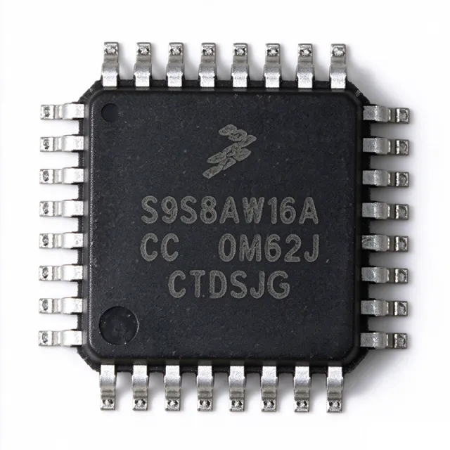
S9S08AW16AE0MLC - 8-bit HCS08 MCU, 16KB Flash, CAN, LQFP-32 | NXP
S9S08AW16AE0MLC

S9S08AW16AE0MLC - 8-bit HCS08 MCU, 16KB Flash, CAN, LQFP-32 | NXP

The NXP S9S08AW16AE0MLC is an 8-bit HCS08 microcontroller unit (MCU) from the low-cost, high-performance MC9S08AW family, integrating a 40 MHz enhanced S08 CPU core with 16 KB of on-chip Flash memory, 1 KB of RAM, and an integrated CAN 2.0 A/B controller. The automotive-grade part is housed in a 32-pin LQFP (7 x 7 mm) package and operates across a -40 C to +125 C temperature range suitable for under-hood and chassis automotive subsystems. Part of the AW16 subset (which also includes AW32, AW48, and AW60 die variants), the S9S08AW16AE0MLC provides HCS08 CPU performance with a 20 MHz internal bus frequency and HC08 instruction set compatibility plus BGND, the new BGNDBG and tagged-breakpoint extensions for modern in-circuit debug. What is an 8-bit HCS08 microcontroller? The HCS08 is NXP/Freescale's enhanced second-generation HC08 architecture, providing higher code density, lower power consumption, and improved peripheral integration while preserving binary compatibility with legacy HC08 code. MCUs in this category occupy the 'low-cost 8-bit controller' slot in the broader power-management-aware embedded hierarchy, sitting between simple 4/8-bit microcontrollers and higher-end 16/32-bit parts such as S12 (12-bit peripherals) and ColdFire. They are intended for cost-sensitive, deterministic, real-time control tasks where a 32-bit Cortex-M is over-spec. Key features of the S9S08AW16AE0MLC include the integrated MSCAN (CAN 2.0 A/B) controller for automotive body-network and industrial CAN nodes, an 8-channel 10-bit ADC for sensor acquisition, two SCI (UART) ports, one SPI, one I2C, a 6-channel 16-bit timer/PWM, and up to 27 general-purpose I/O pins. The device integrates a 3.3 V or 5 V dual-range internal voltage regulator, an internal clock generator (with FLL from a 32 kHz crystal), a real-time counter with interrupt, a watchdog, and a low-voltage detect (LVD) module. Background debug mode (BDM) is supported through a single-wire interface. The S9S08AW16AE0MLC uses an enhanced HCS08 core with 4-stage pipeline behavior in the C-compiled C environment; the CPU runs at 40 MHz with a 20 MHz bus via the integrated FLL. Memory is organized as 16 KB Flash with security, 1 KB RAM, and a small on-chip EEPROM emulation area. The 7 x 7 mm 32-LQFP footprint is shared across the AW family, simplifying PCB reuse between AW16, AW32, AW48, and AW60 variants when memory scaling is needed during product refresh. Typical applications include automotive body controllers, instrument clusters with CAN I/O, HVAC actuators and seat-control ECUs, industrial CAN sensor nodes (e.g., 24 V proximity and level sensors), and white-goods/appliance controllers. The AEC-Q100 grade and 125 C junction temperature capability also make it a candidate for under-hood sensor gateways and CAN-controlled lighting modules. When designing with the AW16AE0MLC, place an external 32.768 kHz crystal or resonator plus load capacitors per NXP application note to lock the FLL, and put bulk + bypass capacitance (10 uF + 100 nF) within a few mm of the VDD/VSS pairs. Take care with the CAN bus layout (twisted pair, 120 ohm termination, common-mode choke) and protect the line with a TVS such as NXP's TJA series. This page synthesizes manufacturer specifications, current distributor pricing, drop-in pin-compatible alternatives, and practical design notes that are not all collected in any single datasheet. Field

Запрос цены Контакты
S9S08AW16AE0VLD - 8-bit MCU, 16KB Flash, 40MHz, Auto QFP-44 | NXP
S9S08AW16AE0VLD

S9S08AW16AE0VLD - 8-bit MCU, 16KB Flash, 40MHz, Auto QFP-44 | NXP

The NXP S9S08AW16AE0VLD is an 8-bit microcontroller from the HCS08 family featuring a 40 MHz S08 core, 16 KB of on-chip Flash, 1 KB RAM and an integrated ADC, packaged in a 44-pin LQFP (10x10 mm) and qualified to -40 / +105 °C for automotive applications. It is a member of the low-cost, high-performance MC9S08AW60/AW48/AW32/AW16 series, the AW16 being the lowest-memory variant of the family. The 'S9' prefix and 'A' suffix designate the automotive temperature grade and the on-chip analog module set. A microcontroller (MCU) is a single-chip computer that integrates a CPU, memory (Flash/RAM), and programmable peripherals such as timers, ADC, serial interfaces, and I/O ports. The HCS08 CPU core is the successor to the legacy HC08 core and executes the same instruction set with the addition of the BGND instruction for background debug mode. The S9S08AW16AE0VLD sits in the broader taxonomy: 8-bit MCU -> HCS08 family -> Freescale/NXP automotive MCUs -> embedded microcontrollers -> semiconductors. Key features of the S9S08AW16AE0VLD include a 20 MHz internal bus frequency, single-wire background debug mode (BDM) interface with breakpoint capability for in-circuit debugging, an integrated voltage regulator for wide-range supply operation, multiple low-power stop and wait modes, a 10-bit or 12-bit ADC (per family datasheet), and a full set of timers, SCI, SPI and I/O peripherals. The 44-pin LQFP gives 30+ general-purpose I/O lines suitable for body-electronics and sensor-interface designs. The device uses a CISC HCS08 core with a 3-stage pipeline, providing deterministic interrupt latency and code-efficient HC08-compatible instructions. The internal clock generator and integrated voltage regulator simplify power-tree design, while the on-chip Flash supports in-application reprogramming via the BDM interface, useful for field firmware updates. Typical applications include automotive body controllers, HVAC control modules, instrument cluster sub-MCUs, sensor interfaces, and low-cost industrial control nodes. Its automotive temperature grade and BDM debug make it well suited for production-line programming and end-of-line calibration. When designing with this MCU, ensure that the BDM pins are reserved for debug access or properly pulled to a defined state in production. The 44-pin LQFP requires thermal vias under the exposed pad footprint variant (if present) to meet the 105 °C automotive temperature spec. This page synthesizes distributor pricing, drop-in alternatives from the same NXP S08 family, and practical design notes not found in the bare datasheet - enabling faster component selection, BOM risk assessment, and second-source planning.

Запрос цены Контакты
S9S08AW16AE1CLDR - 8-bit S08 MCU 16KB Flash 40MHz | NXP
S9S08AW16AE1CLDR

S9S08AW16AE1CLDR - 8-bit S08 MCU 16KB Flash 40MHz | NXP

The NXP S9S08AW16AE1CLDR is an 8-bit S08 CISC microcontroller with 16KB of Flash, 1KB of RAM, and a 40 MHz bus clock, housed in a 44-pin LQFP (10x10 mm) package. It is part of the MC9S08AW family of low-cost, high-performance HCS08 microcontrollers, qualified to AEC-Q100 for automotive and industrial applications, and operates across -40 C to +85 C with 3.3 V/5 V supply. An 8-bit microcontroller (MCU) is a single-chip computer that integrates a CPU, RAM, Flash program memory, and a set of peripheral modules (timers, ADC, communication ports) in one package. The S08 core from NXP/Freescale is a popular 8-bit architecture positioned between the older HC08 and 32-bit ColdFire families, providing a cost-effective solution for body electronics, sensor conditioning, motor control, and human-machine interface (HMI) applications. MCUs in this class are sometimes called CISC MCUs or general-purpose microcontrollers, and they sit at the bottom of the embedded computing hierarchy: 8-bit MCU -> 16-bit MCU -> 32-bit MCU -> microprocessor -> SoC. Key features of the S9S08AW16AE1CLDR include 16KB of embedded Flash with security, 1KB SRAM, an internal oscillator, multiple timers (TPM), an 8-channel 10-bit ADC, SCI/SPI/I2C communication peripherals, and up to 38 general-purpose I/O pins. The part supports background debug mode (BDM) for in-circuit programming and offers low-power wait and stop modes for battery-friendly designs. The HCS08 core delivers 1.5 to 3 times the performance of the legacy HC08 at the same clock rate, with a 16-bit stack pointer and index register, the BSET/BCLR bit-manipulation instructions, and up to 64KB of addressable linear memory space. The 40 MHz internal bus frequency enables deterministic interrupt response for real-time control loops. Typical applications include automotive body control modules, HVAC control, instrument clusters, lighting controllers, industrial sensor hubs, and white goods. The wide operating voltage range (2.7 V to 5.5 V) and AEC-Q100 qualification make it well suited to 12 V automotive bus systems where transients and temperature swings are routine. When designing with this part, place decoupling capacitors (100 nF plus 4.7 uF bulk) close to VDD/VSS pairs and keep the RESET pin pulled up with a 10 kohm resistor. Background Debug Mode (BDM) requires a 4-pin connector; leave the BKGD pin accessible for firmware development and field updates. This page combines NXP/Freescale official product data, distributor pricing, AEC-Q100 qualification context, and pin-compatible MC9S08AW16 variants in a single engineering reference.

Запрос цены Контакты
S9S08AW32E5CFGE - 8-bit 40MHz 32KB Flash Automotive MCU | NXP
S9S08AW32E5CFGE

S9S08AW32E5CFGE - 8-bit 40MHz 32KB Flash Automotive MCU | NXP

The NXP Semiconductors S9S08AW32E5CFGE is an 8-bit microcontroller from the HCS08 S08 family, featuring a 40 MHz enhanced S08 core, 32 KB of on-chip FLASH program memory and a 44-pin LQFP (10x10 mm) package. The "S9" prefix denotes the automotive-grade qualification, and the device operates across the AEC-Q100 temperature range targeted at underhood and body-electronics applications. An 8-bit microcontroller (MCU) is a single-chip microprocessor optimized for embedded control tasks where low cost, deterministic interrupt response and simple peripheral integration outweigh raw computational throughput. The S08 core sits in NXP's portfolio between the legacy HC08 and the higher-end ColdFire V1 architectures, and is supported by CodeWarrior HC(S)08 / Eclipse-based IDEs plus the Processor Expert component library. Within the broader taxonomy, this part is a microcontroller -> 8-bit MCU -> HCS08 family member -> automotive-grade variant. Key features include 32 KB FLASH (32K x 8), 2 KB RAM, an integrated internal bus clock with a 40 MHz maximum CPU frequency, multiple timer/PWM modules (TPM), an analog-to-digital converter (ADC), serial communication interfaces (SCI/SPI/IIC), and a robust set of I/O ports. The device supports operation from 2.7 V to 5.5 V with brown-out detection and multiple low-power modes (Stop, Wait, Run). On-chip BGND and debug interfaces enable non-intrusive in-circuit programming using standard NXP BDM tools. The S08 core implements a Von Neumann architecture with a 16-bit address space, hardware stack pointer, and the BSET/BCLR bit-manipulation instructions common in NXP/Freescale MCUs. The 40 MHz bus clock yields a minimum instruction cycle of 25 ns and ~ 1.4 MIPS per MHz, suiting event-driven control loops with predictable latency. The internal voltage regulator and clock source reduce external BOM, while FLASH security bits protect firmware IP. Typical applications include automotive body controllers, instrument clusters, HVAC control modules, lighting controllers, seat and mirror modules, and small industrial sensor nodes. The HCS08 instruction set and peripheral set were designed for deterministic real-time control with minimal software overhead, making the part attractive for cost-sensitive automotive ECUs. The wide operating voltage range and extended AEC-Q100 temperature range support 12 V automotive bus environments. When designing with this device, budget carefully between CPU clock and ADC acquisition time, and ensure the supply decoupling network follows NXP application note AN2491 recommendations. Use the BDM interface for development and field firmware updates; route BKGD and RESET carefully to enable production programming without rework. Pin count is 44 in LQFP-44; plan PCB layout with adequate thermal copper even though quiescent dissipation is modest. This page consolidates distributor pricing, drop-in alternatives, and application guidance that complements the manufacturer datasheet.

Запрос цены Контакты
S9S08AW32E5MFGE - 8-bit MCU, 32KB Flash, 40MHz, Automotive | NXP
S9S08AW32E5MFGE

S9S08AW32E5MFGE - 8-bit MCU, 32KB Flash, 40MHz, Automotive | NXP

The NXP S9S08AW32E5MFGE is an 8-bit S08 microcontroller with 32KB Flash, 40 MHz CPU clock, and 34 programmable I/O pins, housed in a 44-pin LQFP (10x10 mm) package. It is part of the low-cost, high-performance HCS08 family designed for automotive and industrial applications, qualified for the -40 to +125 °C automotive temperature range and supported by an integrated voltage regulator for single-supply operation. A microcontroller (MCU) is a single-chip computer that integrates a CPU core, non-volatile program memory (Flash), working memory (RAM), and configurable peripheral blocks (timers, ADC, communication ports). The 8-bit class occupies the low-power, deterministic, low-cost end of the MCU market and remains widely used in body electronics, sensor nodes, and white-goods control where 32-bit performance is unnecessary. Within the broader taxonomy, the S9S08AW32 belongs to: 8-bit MCU -> microcontroller -> embedded processor -> semiconductor. Key features include 32KB of embedded Flash program memory, 2KB of RAM, four on-chip 16-bit timers, an 8-channel 10-bit ADC, PWM outputs, and a hardware watchdog timer (WDT). Communication is provided through one SCI (UART), one SPI, and one I²C port. The integrated low-voltage detect (LVD) and power-on reset (POR) blocks ensure safe startup and brownout behavior in noisy automotive environments. The device runs from a 2.7 V to 5.5 V supply and draws only a few milliamperes at full CPU activity. Architecturally, the S9S08AW32 uses the Freescale-developed HCS08 CPU core with an enhanced instruction set over the legacy HC08, including multiply and divide instructions. The 40 MHz bus rate delivers roughly 20 MIPS, sufficient for real-time control loops at typical automotive PWM and CAN-equivalent signaling rates. Background debug mode (BDM) is supported through a single-wire interface, allowing non-intrusive in-circuit programming and debug with the standard NXP toolchain. Typical applications include automotive body controllers, HVAC actuators, instrument clusters, sensor conditioning nodes, and small motor-control stages for door modules or fan drivers. The part is also found in industrial white-goods control boards, low-end human-machine interfaces, and battery-powered remote-keyless entry transmitters where the wide temperature range and integrated analog make board design straightforward. When designing with this device, ensure the main supply decoupling is sized correctly for the 40 MHz switching current and that unused I/O pins are configured as outputs or pulled to defined states to avoid unnecessary supply current. The integrated voltage regulator simplifies single-supply designs but the analog supply (VDDA) must be filtered separately from the digital supply for best ADC performance. This page combines authoritative distributor pricing, drop-in replacement candidates, and design guidance not consolidated in the original manufacturer datasheet.

Запрос цены Контакты
S9S08AW32E5MFUE - 8-bit S08 MCU, 32KB Flash, 40MHz, 64-QFP | NXP
S9S08AW32E5MFUE

S9S08AW32E5MFUE - 8-bit S08 MCU, 32KB Flash, 40MHz, 64-QFP | NXP

The NXP S9S08AW32E5MFUE is an 8-bit microcontroller built on the HCS08 core, providing 32KB of on-chip Flash, 40MHz CPU performance, and automotive-grade qualification in a 64-pin QFP (14x14) package. It is part of the MC9S08AW60/48/32/16 family, designed for low-cost, high-performance embedded control across industrial and automotive environments. The device operates across -40C to +125C and supports both 3.3V and 5V supply rails for flexible system integration. An 8-bit microcontroller (MCU) is a compact embedded processor that integrates a CPU core, memory (Flash/RAM), and peripheral interfaces onto a single silicon die. The HCS08 core belongs to the broader category of 8-bit CISC microcontrollers, which sit hierarchically below 32-bit ARM Cortex-M devices in performance but above simple state machines in capability. Within NXP's portfolio, the S08AW family targets cost-sensitive, real-time control applications where deterministic interrupt response and low power matter more than raw compute throughput. The S9S08AW32E5MFUE integrates 32KB of Flash program memory, 2KB of RAM, and a rich peripheral set including timers, ADC, SCI/SPI/I2C communication modules, and an on-chip CAN controller suited for automotive networks. Its 40MHz bus clock delivers 20MHz instruction rate with the HCS08's enhanced 8-bit pipeline, providing predictable deterministic execution for motor control loops. Internal clock generation, watchdog timer, and low-voltage detection enhance robustness in safety-critical systems. The device is fabricated on an automotive-qualified process and is specified across the full -40C to +125C automotive temperature range. The 64-pin QFP (14x14) package offers generous I/O count with surface-mount manufacturability, while the HCS08 core's CISC instruction set keeps code density high and compiler overhead low. On-chip debug and Flash programming support simplify field updates and production testing. Typical applications include automotive body controllers, HVAC actuators, instrument clusters, CAN node endpoints, industrial sensor hubs, and small motor drives. The combination of CAN, ADC, and PWM-rich timers makes the S9S08AW32 particularly well suited to distributed in-vehicle networks. Compact embedded systems in industrial automation, such as valve controllers or remote sensor nodes, also benefit from the part's rugged temperature range and peripheral integration. When designing with the S9S08AW32E5MFUE, ensure decoupling capacitors are placed close to the supply pins and that the CAN bus termination and ESD protection follow IEC 62228 guidelines for automotive network reliability. Always program the Flash configuration section to lock unused pins and configure the watchdog for fail-safe operation in safety-relevant applications. This page synthesizes distributor pricing, drop-in alternatives from the S9S08AW family, and practical design notes not found in the manufacturer datasheet, providing engineers with the information needed to specify, source, and qualify this automotive MCU.

Запрос цены Контакты
S9S08AW32E5MPUE - Automotive 8-bit MCU, 32KB Flash, 40MHz | NXP
S9S08AW32E5MPUE

S9S08AW32E5MPUE - Automotive 8-bit MCU, 32KB Flash, 40MHz | NXP

The NXP S9S08AW32E5MPUE is an automotive-qualified 8-bit microcontroller built on the enhanced HCS08 S08 core, integrating 32KB of on-chip Flash program memory and 2KB of RAM, operating at up to 40 MHz across a -40C to +125C automotive temperature range and housed in a 64-pin LQFP (10x10 mm) package. The device provides 54 general-purpose I/O lines, making it suitable for body electronics and industrial embedded control applications requiring abundant digital interfaces. An 8-bit microcontroller (MCU) is a single-chip computer that integrates a CPU, program memory (Flash/ROM), data memory (RAM), and peripherals on a single die. The S08 family sits within NXP's broader HCS08 product hierarchy: HCS08 family -> S08 core -> AWx sub-family -> specific device (AW32). These MCUs are designed for cost-sensitive, deterministic real-time control where 32-bit performance is overkill but 4-bit too limited. Compared to discrete logic, an 8-bit MCU consolidates timing, decision logic, and peripheral control into one reprogrammable device, reducing PCB area and BOM cost. Key features of the S9S08AW32E5MPUE include its 32KB Flash program memory (32K x 8), 2KB SRAM, an enhanced S08 core with the standard HCS08 instruction set, on-chip peripherals LVD (Low-Voltage Detect), POR (Power-On Reset), PWM, and WDT (Watchdog Timer), plus connectivity through I2C, SCI (UART), and SPI buses. The -40C to +125C operating range and automotive qualification ("E5" suffix) make this MCU well suited for under-hood and chassis ECUs that must endure harsh thermal and electrical environments. Architecturally, the S9S08AW32 uses NXP's S08 enhanced core with up to 40 MHz internal bus speed, internal Flash with security features, and an integrated clock module with an internal oscillator option. The wide operating voltage typically supports 2.7V-5.5V operation, allowing direct connection to 5V automotive rails without additional level shifting. Typical applications include automotive body and chassis controllers, HVAC control modules, instrument cluster sub-processors, industrial sensor interface boards, and low-end CAN/LIN slave nodes. The 54 I/O count is particularly well matched to multi-switch and multi-LED front-panel interfaces. When designing with this device, allocate adequate decoupling (100 nF + bulk) close to the VDD pins, configure the watchdog timer for safety-critical loops, and verify that the operating voltage range covers cold-crank and load-dump transients common in 12V automotive systems. This page synthesizes distributor pricing, drop-in alternatives, and practical design notes not found in the manufacturer datasheet alone.

Запрос цены Контакты
S9S08AW32E7VFGE - 8-bit S08 MCU, 32KB Flash, 40MHz | NXP
S9S08AW32E7VFGE

S9S08AW32E7VFGE - 8-bit S08 MCU, 32KB Flash, 40MHz | NXP

The NXP Semiconductors S9S08AW32E7VFGE is an 8-bit microcontroller unit based on the enhanced S08 (HCS08) core, operating at up to 40 MHz bus frequency, with 32 KB of Flash program memory, qualified for automotive applications across -40C to +105C, housed in a 44-pin LQFP (10x10 mm) package. The S9 prefix denotes NXP automotive-grade temperature and quality screening of the MC9S08AW32 family member. An 8-bit MCU is a microcontroller whose CPU processes data in 8-bit words, combining processor core, program memory (Flash), RAM, and peripherals such as timers, serial interfaces (SCI, SPI, IIC), and ADC on a single chip. Within the product hierarchy, the S08 core sits inside the HCS08 8-bit MCU family, which belongs to the broader microcontroller and embedded processor category of semiconductors. Key features include the low-cost, high-performance HCS08 architecture shared with the MC9S08AW60, MC9S08AW48, MC9S08AW32, and MC9S08AW16 family members; 32 KB (32K x 8) of on-chip Flash memory; a 40 MHz maximum core/bus clock; and automotive qualification supporting under-hood-adjacent temperature environments from -40C to +105C. The 44-LQFP package with gull-wing terminals provides a square 10x10 mm footprint suitable for surface-mount assembly. Technically, all AW-family MCUs use the enhanced S08 core with a variety of module sets, memory sizes, and package options, allowing designers to scale Flash from 16 KB to 60 KB within the same architecture. This makes firmware porting straightforward when moving between memory density points in the family. Typical applications include automotive body electronics, window/door modules, HVAC control, industrial control systems, and consumer appliances where a cost-sensitive 8-bit controller with automotive screening is required. A key design consideration: this part is listed as End of Life (EOL) by NXP, so new designs should verify remaining distributor stock or plan a family migration path. This page synthesizes distributor availability data, lifecycle status, and drop-in alternatives from the same S08AW family - information not consolidated in the manufacturer datasheet.

Запрос цены Контакты