Микросхемы памяти
Подкатегории
Товары (459)

N25Q016A11ESCA0F - 16Mbit SPI NOR Flash 108MHz | Micron Technology
The Micron Technology N25Q016A11ESCA0F is a 16 Mbit serial NOR flash memory with a standard SPI interface supporting clock rates up to 108 MHz, housed in an 8-pin SOIC (8-SO) package. Part of Micron's N25Q flash family, it provides 2 MB of non-volatile code and data storage with a uniform sector architecture suited for firmware storage in embedded systems. A serial NOR flash memory is a type of non-volatile semiconductor memory that stores data in floating-gate cells arranged so that random access to individual bytes is possible through a serial peripheral interface (SPI). In the memory hierarchy, SPI NOR flash sits below parallel NOR and NAND devices in density, but it offers the simplest hardware connection (4 to 8 pins), true execute-in-place (XIP) capability, and high reliability, making it the default boot memory for microcontrollers and processors. Key features of the N25Q016A11ESCA0F include the 108 MHz maximum SPI clock, support for industry-standard SPI commands, and the small-footprint 8-SO surface-mount package that minimizes board area in cost-sensitive designs. The device uses Micron's advanced NOR process technology for high endurance and long data retention, and the industrial temperature-suffix option supports operation in extended thermal environments. Technically, the device implements a command-based architecture with read, fast read, page program, and sector/block erase instructions, plus status register access for polling program/erase completion. Byte-eraseable subsectors and page programming allow efficient firmware update flows, while the SPI interface with mode 0 and mode 3 support eases integration with virtually any MCU or FPGA SPI controller. Typical applications include BIOS/UEFI boot firmware storage, microcontroller code shadowing, FPGA configuration bitstream storage, networking equipment parameter storage, and set-top box or consumer appliance firmware. The compact SOIC-8 package and simple 4-wire interface make it a natural fit for space-constrained embedded boards. A key design consideration: at 108 MHz operation, signal integrity on the SPI clock and data lines matters - keep traces short and verify hold times, or drop to the dual/quad command set with proper IO2/IO3 (WP#/HOLD#) pin handling to increase throughput. This page synthesizes distributor pricing, verified drop-in alternatives, pinout data, and practical design notes not found on distributor listing pages alone.
N25Q032A11ESEA0F - 32Mb 1.8V SPI NOR Flash | Micron
The Micron Technology N25Q032A11ESEA0F is a 32Mb (32M x 1 / 16M x 2 / 8M x 4) serial NOR flash memory operating at 1.8V (1.7V to 2.0V supply range) with a maximum SPI clock frequency of 108 MHz, housed in an 8-pin SOP2 (8-SOIC) package supplied in tape and reel. Serial NOR flash is a nonvolatile memory category that stores code and data while allowing byte-level random access over a simple SPI bus. In the memory hierarchy it sits alongside SPI NAND and parallel NOR: NOR architecture provides execute-in-place (XIP) capability and very fast random read latency, which is why boot code, firmware, and configuration data for embedded processors are typically stored in serial NOR flash rather than NAND devices. Key features of the N25Q032A include Multiple I/O SPI operation supporting standard, dual (x2), and quad (x4) protocols for bandwidth up to 108 MHz clock rates, 4KB sector erase granularity that reduces erase overhead for parameter storage, and a wide operating temperature range of -40C to +85C for industrial designs. The 1.8V supply reduces active power consumption compared with 3V NOR flash, making it attractive for battery-powered and portable systems. Technically, the device uses Micron's N25Q command set, compatible with standard SPI JEDEC-style instructions including FAST_READ, dual/quad output reads, page program, and sector/block erase. A JEDEC-standard SFDP serial flash discoverable parameter table and unique device ID simplify driver integration and multi-vendor socketing. The E-die (ESEA) generation offers improved erase and program performance over earlier A-die versions. Typical applications include firmware/boot code storage for microcontrollers and FPGA configuration (Xilinx, Intel/Altera, Lattice), networking equipment such as routers and switches, industrial automation controllers, set-top boxes, and display panels. The quad-I/O interface is specifically suited to FPGA bitstream loading where configuration time affects system startup. Design consideration: verify hold-time and deep power-down behavior when substituting across vendors, and place a 100 nF decoupling capacitor directly at the VCC pin; quad mode requires IO2/IO3 to be correctly terminated with pull-ups when the HOLD#/WP# functions are unused. This page adds value beyond the datasheet by synthesizing distributor pricing, drop-in alternatives including the Macronix MX25U3235F cross-reference, and practical substitution notes in one place.

N25Q032A13EF4A0F - 32Mbit SPI NOR Flash 108MHz | Micron
The Micron N25Q032A13EF4A0F is a 32 Mbit (4 MB) automotive-grade serial NOR Flash memory with a 108 MHz SPI multi-I/O interface and 2.7 V to 3.6 V supply range, housed in an 8-contact UFDFPN (MLP8) package measuring 4 x 3 mm. The device supports standard, dual, and quad SPI protocols, enabling read bandwidths up to 432 MB/s-equivalent in quad mode at full clock speed. Serial NOR Flash is a type of non-volatile memory that stores code and data while allowing random-access reads over a simple SPI bus using just a handful of pins. It sits at the lower end of the memory hierarchy relative to parallel NOR, NAND Flash, and DRAM, and is the dominant boot-memory technology for embedded processors, microcontrollers, FPGAs, and networking SoCs. Key features include the 108 MHz maximum clock frequency with 03h/0Bh fast-read commands, dual-output (3Bh), dual-I/O (BBh), quad-output (6Bh), and quad-I/O (EBh) read modes, an erase granularity down to 4 KB subsectors, and block protection for code-security-critical applications. The EF4 package option offers an industrial-plus/automotive operating temperature profile, and the A0F ordering code denotes Micron automotive program units. Architecturally, the N25Q family uses a single-die array organized as 64 sectors of 64 KB (each subdividable into 4 KB subsectors) with a command set compatible across Micron N25Q and MT25Q generations, simplifying second-source migration within the vendor roadmap. Endurance and retention follow Micron data-erase program cycling specifications for serial NOR. Typical applications include BIOS/UEFI boot storage on x86 embedded and industrial platforms, FPGA configuration storage for Xilinx and Intel devices, automotive infotainment and telematics firmware, and networking equipment code storage, where the 108 MHz quad-mode read speed shortens boot time. Design consideration: always verify whether your host expects the N25Q (extended SPI) versus the later MT25QL/MT25QU command set, and budget a 10 uF plus 0.1 uF decoupling pair at VCC to support program/erase surge currents. This page adds value beyond the raw datasheet by consolidating distributor pricing, drop-in alternatives from Micron and cross-brand vendors, pinout data, and practical design notes in one citation-friendly reference.
N25Q032A13ESCA0F - 32Mb SPI NOR Flash 108MHz | Micron
The Micron N25Q032A13ESCA0F is a 32Mbit (4M x 8) SPI-compatible serial NOR flash memory operating from a 3V (2.7V to 3.6V) supply at up to 108 MHz clock frequency, housed in an 8-pin SOIC (SO) package supplied on tape and reel. It supports Standard, Dual and Quad SPI Multiple I/O protocols, making it suitable for code shadowing, XIP (execute-in-place) boot code and data storage. Serial NOR flash is a non-volatile memory category within the broader flash memory hierarchy (flash memory -> NOR flash -> serial NOR -> SPI memory IC). Unlike parallel NOR, serial NOR uses a compact SPI bus of typically four signal pins, drastically reducing package pin count and PCB routing area. This makes SPI NOR the standard choice for boot code storage in embedded processors, FPGAs and microcontrollers where board space is at a premium. Key features include the 108 MHz maximum clock rate with multiple I/O operation that effectively multiplies bandwidth, a SPI-compatible serial bus interface, and automotive-grade qualification suitable for vehicle-mounted systems. The device supports XIP confirmation bit settings for direct code execution from the flash array, program and erase suspend/resume operations, and defined power-up/power-down requirements with a power-loss rescue sequence for data integrity during brownout conditions. Architecturally, the N25Q family organizes the 32Mb array into uniform sectors and subsectors addressed through standard SPI read, page program, sector erase and bulk erase commands. The enhanced multiple I/O command set and extended address capabilities reduce instruction overhead, while hold and deep power-down modes minimize standby current in battery-sensitive designs. Typical applications include BIOS/boot code storage in networking routers and switches, code storage for embedded FPGA configuration bitstreams (e.g., paired with Intel/Altera SoC FPGAs), automotive body and infotainment modules, and industrial control systems requiring non-volatile firmware storage. When designing with this device, observe the specified power-up timing and include the power-loss rescue sequence handling in your firmware to guarantee array integrity after unexpected power removal. This page synthesizes distributor pricing, drop-in alternatives, and practical design notes not found in the manufacturer datasheet.
N25Q032A13ESEA0F - 32Mb SPI NOR Flash 108MHz | Micron
The Micron Technology N25Q032A13ESEA0F is a 32Mbit serial NOR flash memory operating at 3V (2.7V to 3.6V) with a maximum SPI clock frequency of 108 MHz, organized as 32M x 1 / 16M x 2 / 8M x 4 bits in an 8-pin SOP-II (208 mil, SOP2-8) surface-mount package with tape-and-reel delivery. A serial NOR flash memory is a non-volatile storage IC that stores code and data with random-access read behavior over the Serial Peripheral Interface (SPI). Within the memory hierarchy, NOR flash sits alongside NAND flash under the flash memory family, which in turn belongs to solid-state non-volatile semiconductor memory. Serial NOR is the dominant choice for firmware boot code because it supports execute-in-place (XIP) with short access latency, unlike NAND which requires block-level reads through a controller. Key features of the N25Q032A include its 108 MHz maximum clock rate in standard, dual (2-bit) and quad (4-bit) I/O modes, giving designers up to four times the effective read bandwidth of single-I/O serial flash. The 7 ns access time specification supports fast XIP boot architectures. Its 32Mbit density is organized into uniform sectors supporting erase, program, and flexible protection, and the memory supports erase-suspend and program-suspend operations so that host code can continue executing during background maintenance. The device uses Micron's multiple I/O serial NOR architecture with JEDEC-standard SPI command behavior, deep power-down modes for low standby current, and block-level write protection. The wide -40C to +125C operating temperature range of this suffix enables use in automotive-adjacent, industrial, and outdoor environments where consumer-grade 0C to 70C parts cannot survive. Typical applications include BIOS/UEFI and firmware storage on embedded computing modules, boot flash for FPGAs and microcontrollers (including Microsemi/Microchip RTAX and ProASIC families that need configuration bitstream storage), industrial controllers, networking equipment, and data-logging systems. Design consideration: layout the SPI traces with short, matched lengths and provide a 100 nF ceramic decoupling capacitor close to VCC pin 8; avoid exceeding the specified 3.6V absolute maximum to prevent program/erase reliability degradation. This page synthesizes distributor pricing, drop-in alternatives, pinout data, and practical design notes not found in the manufacturer datasheet, as of 2026-09-02.
N25Q032A13EV7A0 - 32Mb SPI NOR Flash 108MHz | Micron
The Micron Technology N25Q032A13EV7A0 is a 32Mbit SPI NOR Flash memory IC operating at up to 108 MHz clock frequency, supplied at 2.7V to 3.6V, housed in an 8-lead VDFPN8 (MLP8) surface-mount package. NOR Flash is a non-volatile memory type in which each cell connects in parallel to bit lines, enabling true random access for code execution in place (XIP). Within the memory hierarchy, NOR Flash sits alongside NAND Flash under non-volatile semiconductor memory; where NAND stores bulk data, NOR Flash stores boot code and firmware that microprocessors execute directly from the array. SPI (Serial Peripheral Interface) NOR devices reduce pin count versus parallel NOR, simplifying board routing for embedded designs. Key features of the N25Q032A13EV7A0 include the 32Mbit (4MB) density organized for 8M x 4 die, a 108 MHz maximum SPI clock supporting double data rate and dual/quad I/O operation for fast code download, and a wide 2.7V to 3.6V supply range compatible with standard 3.3V systems. The device supports industrial-grade temperature from -40C to +125C per distributor data, allowing use in harsh environments. Architecturally, this device belongs to Micron's N25Q (P-Stim / e-Memory) family of high-performance SPI NOR Flash, which adds paging support, subsector erase granularity and fast program/erase timing. Standard commands cover read, page program, sector and bulk erase with status polling via the status register. Typical applications include firmware and boot code storage for industrial controllers, networking equipment configuration memory, automotive infotainment modules, and set-top box boot devices where reliable XIP execution is required. Design consideration: keep SPI clock loading low and add series damping resistors on SCK when running at 108 MHz to limit signal integrity issues; verify erase/program cycles against the specified endurance in the manufacturer datasheet. This page synthesizes distributor availability, drop-in family alternatives, and practical design notes not found in the manufacturer datasheet.

N25Q064A11E12A0F - 64Mb SPI NOR Flash 1.8V 108MHz | Micron
The Micron Technology N25Q064A11E12A0F is a 64Mb (8 MB) 1.8V multiple I/O serial NOR flash memory with a 108 MHz SPI clock rate, packaged in a 24-ball T-PBGA (6x8 mm) surface-mount package and rated for -40C to +125C operation. Serial NOR flash is a nonvolatile memory category that stores code and data while allowing byte-level random access over a serial peripheral interface (SPI). Within the memory hierarchy, NOR flash sits alongside NAND flash and DRAM as a core memory IC, and its execute-in-place (XIP) capability makes it the default boot-code storage for embedded processors, microcontrollers, and FPGAs. Multiple I/O (dual and quad SPI) variants increase effective bandwidth without widening the physical footprint. Key features include 64Mb SLC NOR density organized as 16M x 4, a 108 MHz maximum SPI clock that supports double data rate operation for higher throughput, a wide 1.7V to 2.0V supply range, and an industrial-to-automotive operating temperature range of -40C to +125C. The device supports single, dual, and quad I/O commands plus memory-mapped XIP execution, allowing hosts to boot code directly from flash. Technically, the N25Q family uses single-level-cell NOR technology with sector and subsector erase granularity, block protection, and standard JEDEC SFDP serial flash discoverable parameters for host enumeration. The 24-ball T-PBGA footprint is compact for board layouts where routing a wide parallel bus would be impractical. Typical applications include boot firmware storage for FPGAs and SoCs in automotive and industrial systems, BIOS/UEFI code storage in networking equipment, configuration data for embedded displays, and firmware repositories in telematics and telematics-adjacent modules. A key design consideration is SPI signal integrity: at 108 MHz, keep clock and data traces short and matched, and verify that the host controller supports the N25Q command set or an SFDP-driven driver. Budget erase times when planning field firmware updates. This page synthesizes distributor pricing, drop-in alternatives, and practical design notes not found in the manufacturer datasheet.
N25Q064A13E12A0F - 64Mb SPI NOR Flash 108MHz | Micron
The Micron Technology N25Q064A13E12A0F is a 64 Mbit (8 MB) 3V multiple I/O SPI serial NOR flash memory operating up to 108 MHz and housed in a 24-ball T-PBGA (6x8 mm) package. A serial NOR flash memory is a nonvolatile storage device organized so the CPU can execute or read code directly from individual byte-addressable locations over a serial peripheral interface. Within the memory hierarchy, NOR flash sits between EEPROM and parallel NAND flash, offering random access with fast read latency but lower density and higher cost per bit than NAND. Serial NOR devices connect to a host MCU or FPGA through an SPI bus, making them the de facto standard for boot code storage in embedded systems. Key features of the N25Q064A family include standard, dual, and quad SPI protocol support, effectively multiplying bandwidth when using 2-bit or 4-bit I/O. The 108 MHz clock rate enables read throughput suitable for XIP (execute-in-place) code shadowing without copying to RAM. The device supports sector and bulk erase operations, hardware and software write protection, and XIP mode activation per the manufacturer datasheet. Technically, the part is organized as 64 Mbit accessed over a 3.0 V supply range, with the A13 speed/temperature suffix indicating the commercial operating envelope. Programmable sector protection and suspend/resume of program-erase operations allow background updates without stalling code reads, which matters in systems where flash is shared between boot code and data logging. Typical applications include MCU boot firmware storage in industrial automation, FPGA configuration memory in networking and communications equipment, and code storage in embedded computing and consumer platforms where board space and pin count favor serial interfaces. Design considerations: respect power-up sequencing requirements and the power-loss rescue sequence described in the manufacturer datasheet, and follow recommended decoupling to avoid brown-out corruption during erase operations. This page adds value beyond the datasheet by synthesizing distributor availability data, same-family drop-in alternatives, pricing context, and practical design notes for engineering and procurement teams.
N25Q064A13EF8A0E - 64Mb SPI NOR Flash 108MHz | Micron
The Micron N25Q064A13EF8A0E is a 64 Mb (8 MB) 3 V multiple I/O serial NOR Flash memory supporting SPI clock rates up to 108 MHz, manufactured on 65 nm NOR technology and housed in an 8-pin VDFPN (MLP8, 8 x 6 mm) exposed-pad package. A serial NOR Flash is a nonvolatile memory device that stores code and data and is read over a serial bus (SPI) using a memory-mapped execute-in-place (XIP) model. In the system hierarchy, NOR Flash occupies the code-storage tier between boot ROM and DRAM/NAND mass storage, providing random access for direct code execution without copying to RAM first. Key features of the N25Q064A13EF8A0E include 64 Mb density, 108 MHz SPI operation in standard, dual, and quad I/O modes, and an automotive-grade temperature profile. The multiple I/O architecture reduces instruction overhead and improves effective read bandwidth compared to single-I/O SPI Flash, accelerating boot times in embedded processors. The exposed-pad DFN package provides good thermal and electrical grounding and a compact 8 x 6 mm footprint. Technically, the device uses 65 nm NOR floating-gate technology with sector and block erase organization, program/erase suspend capability, and XIP modes that allow the host controller to execute code directly from the Flash array. Power-up and power-down behavior, rescue sequences, and AC reset specifications are fully documented in the manufacturer datasheet to ensure deterministic system startup. Typical applications include BIOS/code storage in embedded x86 and ARM systems, boot firmware for networking equipment, automotive telematics and infotainment modules, and FPGA configuration storage where quad-SPI read bandwidth shortens configuration time. Design consideration: keep SPI trace lengths short and matched for quad-I/O operation at 108 MHz, and verify power-up timing against the datasheet power-up requirements to avoid false device lockout states. This page synthesizes distributor pricing, verified drop-in alternatives, pinout data, and practical design notes in one place - information not consolidated in the manufacturer datasheet alone.
N25Q064A13ESEA0F - 64Mb SPI NOR Flash 108MHz | Micron
The Micron Technology N25Q064A13ESEA0F is a 64Mb (8 MB) 3V multiple I/O serial NOR flash memory with a maximum SPI clock frequency of 108 MHz, housed in an 8-pin wide SOIC (SOP-8 W) package. It supports standard, dual, and quad SPI protocols (1-bit, 2-bit, and 4-bit I/O), making it a versatile code-storage solution for embedded systems. Serial NOR flash is a non-volatile memory technology that stores code and data without power, accessed over a simple serial peripheral interface (SPI) using a clock line, chip select, and one to four data lines. In the memory hierarchy, it sits below parallel NOR and NAND flash in interface complexity, which makes it the standard choice for firmware boot storage in microcontroller and processor-based systems. Key features include the 64 Mb density organized as 64M x1, 32M x2, or 16M x4 depending on the protocol, fast 108 MHz clock operation for high read throughput, and the extended address command set suitable for devices above 128 Mb capacity. The part supports execute-in-place (XIP) mode, allowing the host processor to run code directly from the flash, plus program and erase suspend/resume for responsive systems and power-up/power-down sequencing protections. Architecturally, the N25Q (EXPERT family) uses Micron NOR flash cells with sector and block granularity for erase operations and page programming. Hardware and software reset support, XIP activation control, and a power loss rescue sequence protect data integrity during brownout conditions. The 3V supply (2.7V to 3.6V class) suits both portable and line-powered designs. Typical applications include firmware boot memory for embedded controllers, data logging in industrial equipment, BIOS/UEFI storage in computing modules, and configuration storage in networking hardware. When designing with this device, follow the datasheet power-up and power-down requirements and add decoupling capacitors close to VCC to maintain data integrity during transients. This page synthesizes verified distributor data, same-footprint drop-in alternatives, pinout detail, and practical design notes not found in the manufacturer datasheet.

N25Q064A13ESFA0F - 64Mb 108MHz SPI NOR Flash | Micron
The Micron Technology N25Q064A13ESFA0F is a 64Mb (8 MB) 3V multiple-I/O SPI serial NOR flash memory with a maximum clock rate of 108 MHz and a 16-pin SOIC wide body (400-mil) package. It supports standard SPI, dual SPI, and quad SPI interfaces, and is qualified to AEC-Q100 for automotive applications with an operating temperature range of -40C to +125C. Serial NOR flash is a nonvolatile memory technology that stores code and data in a NOR array accessible over a simple serial peripheral interface. Within the memory hierarchy, it sits alongside parallel NOR and NAND flash as a member of the flash memory family, and is the dominant choice for boot code storage because it offers random-access read behavior, high reliability, and XIP (execute-in-place) capability from a very small pin count. Key features of this device include 64Mb density organized as 64M x 1, 32M x 2, or 16M x 4 depending on the interface mode; a 4KB sector erase granularity that reduces erase overhead for parameter storage; and quad I/O operation that delivers effective read bandwidth far beyond legacy single-bit SPI. An accelerated program/erase path and deep power-down mode minimize system power, and hardware RESET# support improves system recoverability. Technically, the N25Q family uses advanced NOR floating-gate cells with 3V single-supply operation. Command set compatibility with the widely used 25-series convention, page programming, block (64KB) and sector (4KB) erases, and status-register-based polling simplify driver development. The device also supports XIP mode activation with confirmation bit settings, as described in the manufacturer datasheet. Typical applications include automotive ECU boot code storage, firmware storage for industrial PLCs and networking equipment, BIOS storage in embedded x86 systems, and parameter storage in medical and test instruments. The 108 MHz quad SPI interface makes it well matched to MCUs and SoCs with quad-SPI memory controllers. Design consideration: verify that the controller drive strength and PCB trace length support 108 MHz quad SPI signaling, and always reserve access to RESET# for field recoverability. This page synthesizes distributor pricing context, drop-in alternative analysis, pinout, and practical design notes not found in the manufacturer datasheet alone.
N25Q128A13EF8A0F - 128Mb SPI NOR Flash 108MHz | Micron
The Micron N25Q128A13EF8A0F is a 128-Mbit (16 MB) 3V multiple I/O serial NOR flash memory with a 108 MHz SPI bus interface, housed in an 8-pin VDFPN (MLP8, 8x6 mm) package with exposed pad. It supports SPI, dual SPI (DIO), and quad SPI (QIO) protocols, enabling XiP (execute-in-place) operation at up to 108 MHz. Serial NOR flash is a nonvolatile memory category within the broader flash memory hierarchy (nonvolatile memory -> flash -> NOR flash -> serial SPI NOR flash). Unlike parallel NOR, serial NOR uses a compact SPI interface that saves board space and pin count, making it the standard code-storage medium for embedded processors, FPGAs, and microcontrollers. The N25Q family (originally developed by Numonyx B.V., now Micron Technology) is a widely validated XiP-enabled boot flash platform. Key features include 4-Kbyte subsector erase granularity for efficient parameter and data storage, a 3V/3.3V supply (2.7V to 3.6V), operating temperature of -40C to +125C for industrial environments, and fast access with 7 ns output timing noted in distributor data. The 128 Mbit density is organized as 16M x 8 in the SLC configuration listed by Mouser. Architecturally, the device divides the 128 Mb array into 4-Kbyte subsectors and 64-Kbyte sectors, supporting single, dual, and quad I/O command sets that reduce instruction overhead and boost effective bandwidth in XiP applications. Quad I/O transfers over DQ0-DQ3 with the 108 MHz clock deliver high throughput for FPGA configuration image loading and embedded code execution. Typical applications include FPGA configuration storage (notably Xilinx 7-series and Intel/Altera SoC boot designs), embedded processor code shadowing, and industrial communication-module firmware storage. Its -40C to +125C range suits automotive-adjacent and factory environments. Designers should note that the exposed pad of the VDFPN-8 package must be soldered for thermal and ground integrity, and 100 nF decoupling close to VCC pin 2 is recommended. Programmer support exists in most mainstream SPI programmers, and command-set compatibility within the N25Q family simplifies migration between densities. This page synthesizes distributor pricing data, verified drop-in alternatives, pinout details, and practical design notes not consolidated in the manufacturer datasheet.
N25Q128A13ESFA0F - 128Mb SPI NOR Flash 108MHz | Micron
The Micron Technology N25Q128A13ESFA0F is a 128 Mbit (16 MB) 3 V multiple-I/O serial NOR flash memory with a 108 MHz SPI bus interface, 4-Kbyte subsector erase granularity, and XiP (execute-in-place) support, housed in a 16-pin wide-body SOIC (SO W, 300 mil) surface-mount package. Serial NOR flash is a nonvolatile memory category that stores code and data while allowing byte-level random access over a serial peripheral interface. Within the memory hierarchy, it sits between parallel NOR flash (faster but pin-hungry) and serial NAND (cheaper but block-accessed). Serial NOR is the dominant boot-memory choice for embedded processors because code can execute directly from the array (XiP) or be shadowed to RAM at power-up, with only four to six signals required. Key features of the N25Q128A13ESFA0F include 128 Mbit density organized as 16M x 8, support for standard, dual, and quad SPI protocols that double and quadruple effective bandwidth, 4-Kbyte subsector erase on boot sectors for fine-grained parameter storage, and a clock speed up to 108 MHz with fast access time (7 ns class per distributor listings). The device operates from a single 3V/3.3V supply, supporting the standard industrial memory rail. Architecturally, the N25Q family (originally developed by Numonyx, later acquired by Micron) uses a multi-I/O SPI front end with command-set compatibility extended for dual-output, dual-I/O, quad-output, and quad-I/O read modes. This lets host controllers trade pin count for throughput: quad-I/O operation at 108 MHz yields an effective transfer rate several times higher than conventional single-SPI serial flash, enough to meet XiP boot-time targets in embedded Linux and RTOS systems. Typical applications include code storage for FPGAs and CPLDs, boot flash for embedded processors and SoCs, BIOS/firmware storage in networking equipment, and configuration memory in industrial automation and telecommunications line cards. The quad-SPI interface and XiP support make it a natural match for Xilinx-style configuration streams and memory-mapped execution on Cortex-class MCUs. Design consideration: when running quad-I/O reads at 108 MHz, keep SPI trace lengths short and matched, and verify that the HOLD#/DQ3 pin is driven correctly, because in quad mode it functions as an active data line rather than a hold control. This page synthesizes distributor pricing, drop-in alternatives, pinout guidance, and practical design notes not found in the manufacturer datasheet, and is verified as of 2026-09-02.
N25Q256A13E12A0F - 256Mb SPI NOR Flash, 108MHz | Micron
The Micron Technology N25Q256A13E12A0F is a 256Mb (32MB) Multiple I/O Serial NOR Flash memory operating at 2.7V to 3.6V, supporting an SPI clock of up to 108 MHz in a 24-ball T-PBGA (6x8 mm) package. It uses SLC (single-level cell) technology and is rated for operation from -40C to +125C. Serial NOR Flash is a nonvolatile memory category within the flash memory hierarchy (NOR Flash -> serial NOR Flash -> SPI Flash -> nonvolatile semiconductor memory). Unlike parallel NOR or NAND Flash, serial NOR devices communicate over a compact SPI bus (with single, dual, and quad I/O modes in this Multiple I/O family), which dramatically reduces pin count, PCB area, and routing complexity. This makes SPI NOR Flash the de facto standard for code storage (XIP, execute-in-place) next to microcontrollers, FPGAs, and networking processors. Key differentiating features of the N25Q256A13E12A0F include its 256Mb density, 108 MHz SPI clock rate (enabling quad I/O transfers for high read throughput), 4KB sector erase granularity for efficient in-field firmware updates, and an industrial-to-automotive-adjacent -40C to +125C operating range. The 24-ball T-PBGA (6x8) footprint keeps the memory close to the host processor for signal integrity at high clock rates. Technically, the device is part of the Micron N25Q Multiple I/O Serial Flash family, which adds dual-output/dual-I/O and quad-output/quad-I/O SPI commands on top of standard single-I/O SPI. The 4KB sector organization (as stated in the 3V, 256Mb Multiple I/O Serial Flash datasheet) allows fine-grained erase before program, which is important for parameter storage blocks that coexist with a large boot image. SLC architecture provides higher endurance and wider temperature margin than multi-level cell alternatives. Typical applications include FPGA configuration storage, BIOS/UEFI boot code in embedded x86 platforms, firmware storage in industrial drives and networking line cards, and automotive infotainment clusters needing reliable code execution over temperature. Design consideration: for execute-in-place at 108 MHz, keep SPI traces short and matched; for maximum throughput in code-shadowing scenarios, prefer quad I/O commands so effective read bandwidth approaches four times the single-I/O SPI rate. This page synthesizes distributor availability data, cross-reference findings, and practical design notes not found in the manufacturer datasheet alone.
N25Q256A13EF8A0F - 256Mb SPI NOR Flash 108MHz | Micron
The Micron N25Q256A13EF8A0F is a 256Mb (32MB) 3V multiple I/O serial NOR Flash memory delivering up to 108 MHz SPI clock operation in an 8-pin VDFPN (MLP8, 8x6 mm) package. It supports x1, x2, and x4 I/O width via single, dual, and quad SPI protocols, and operates from -40C to +85C. Serial NOR Flash is a nonvolatile memory category that stores code and data while allowing byte-level random read access over a simple serial peripheral interface. In the system hierarchy it sits below parallel NOR and NAND Flash in pin count and board area, making it the dominant boot-memory choice for embedded processors, microcontrollers, and FPGAs where a compact footprint and high reliability outweigh raw density. Key features include 108 MHz maximum clock frequency with 8 ns access timing, 4KB sector erase granularity that reduces update latency and wasted erase cycles, multiple I/O (SPI, dual-SPI, quad-SPI) protocols that cut instruction overhead and boost effective read bandwidth, and a 3V to 3.6V single supply. The VDFPN exposed-pad package improves thermal and ground performance over standard SOIC-8 while remaining footprint-compatible in most layouts. The device is manufactured on Micron's 65nm NOR technology, the first generation of Micron's high-performance multiple I/O serial Flash family. Subsector erase of 4KB sectors enables fine-grained parameter storage, while block (64KB) and full-chip erase options support bulk reprogramming. A hardware write-protect pin (W#/VPP_DQ2) allows software-controlled sector locking and protects the boot region against accidental corruption. Typical applications include FPGA configuration bitstream storage, embedded processor boot code, BIOS/UEFI firmware in industrial PCs, automotive instrument clusters, and networking equipment line cards. Quad-SPI mode makes the device especially well matched to Intel/Altera and Xilinx configuration flows. Design consideration: respect the 100K program/erase cycle endurance per sector in firmware by implementing wear-leveling or sector rotation for frequently updated parameters, and decouple VCC with 0.1uF close to pin 2. This page synthesizes verified distributor data, drop-in same-family alternatives, pinout detail, and practical design notes not found in the manufacturer datasheet.
N25Q256A13ESFA0F - 256Mb SPI NOR Flash 108MHz | Micron
The Micron N25Q256A13ESFA0F is a 256 Mbit (32 MB) SPI-compatible serial NOR Flash memory manufactured on 65 nm NOR technology, operating from a 2.7 V to 3.6 V supply at up to 108 MHz in a 16-pin SOP2 (SOP-II) surface-mount package. It supports single, dual, and quad I/O SPI protocols for x1/x2/x4 data widths. Serial NOR Flash is a non-volatile memory class that stores code and data while allowing in-system byte-wise reads through a low-pin-count SPI bus. In the memory hierarchy it sits between parallel NOR (higher pin count, faster random access) and serial NAND or EEPROM (lower endurance, slower random access), making it the default boot memory for embedded processors, microcontrollers, and FPGAs. Key features include a 108 MHz maximum clock frequency with equivalent dual- and quad-I/O throughput, 4 KB sector erase granularity for fine-grained wear management, execute-in-place (XIP) capability so code can run directly from the Flash without copying to RAM, and advanced write-protection mechanisms. The 65 nm SLC NOR cell design delivers high reliability and fast random read latency versus charge-trap alternatives. Architecturally, the N25Q256A device organizes 256 Mbit as 32 M x 8 with sector, subsector, and page program operations, using an SPI-compatible instruction set familiar from the broader N25Q family. The multiple-I/O bus and XIP mode minimize boot time in deeply embedded systems, while the standard SPI commands simplify software reuse across density grades. Typical applications include FPGA and MCU boot code storage, automotive and industrial embedded systems, networking equipment firmware, and set-top-box or display code storage, where 32 MB of reliable code memory with quad-SPI bandwidth is required. Design consideration: when running at 108 MHz in quad mode, pay close attention to signal integrity on DQ lines and keep trace lengths matched; confirm the required output drive and dummy-cycle configuration per the manufacturer datasheet. This page synthesizes distributor pricing context, drop-in same-package alternatives, pinout, and practical design notes not found in a single manufacturer document.
N25Q256A83ESFA0F - 256Mb SPI NOR Flash 108MHz | Micron
The Micron Technology N25Q256A83ESFA0F is a 256 Mbit (32 MB) 3V multiple I/O serial NOR flash memory with an SPI-compatible bus operating at up to 108 MHz, housed in a 16-pin wide SOIC (SOIC-16 W) surface-mount package with industrial operating temperature range of -40C to +125C. A serial NOR flash memory is a non-volatile storage IC that stores code and data on NOR cells and communicates over a serial SPI bus (single, dual, or quad I/O). Within the memory hierarchy, it sits alongside parallel NOR, NAND flash, and EEPROM as a class of non-volatile memory ICs, and is the standard choice for execute-in-place (XIP) boot code because it offers random access with low pin count. Key features of the N25Q256A83ESFA0F include 256 Mbit density organized as 32M x 8, quad SPI (multiple I/O) data throughput at 108 MHz clock rates, 4 KB sector erase granularity for flexible code management, and advanced write-protection mechanisms. The device is manufactured on Micron's 65nm NOR technology, the first generation of the high-performance N25Q family. Architecturally, the N25Q supports execute-in-place (XIP) operation, allowing the host processor to run code directly from the flash without copying to RAM first. The SPI-compatible interface supports standard single-I/O, dual-I/O, and quad-I/O commands, and the extended temperature rating makes the part suitable for harsh industrial environments. Memory array organization uses sectors and subsectors for erase operations and page programming for writes. Typical applications include boot code storage in industrial controllers, embedded processors and FPGAs, networking equipment storing firmware images, and automotive-adjacent telematics or display modules where wide temperature tolerance is required. When designing with this part, verify that your host SPI controller supports the command set and that hold and reset functions are correctly terminated; upper address bits beyond the 24-bit boundary are accessed through extended address registers. Decouple VCC with 0.1uF ceramic capacitors close to pin 2. This page synthesizes distributor pricing, verified specifications, same-family drop-in alternatives, and practical design notes not found together on the manufacturer datasheet alone.

N25Q512A13G12A0F - 512Mb SPI NOR Flash 108MHz AEC-Q100 | Micron
The Micron N25Q512A13G12A0F is a 512 Mbit (64 MB) multiple-I/O serial NOR flash memory with SPI, dual SPI, and quad SPI interfaces, operating from a 3V/3.3V supply, supporting clock speeds up to 108 MHz, in a 24-ball TFBGA (6x8 mm) package qualified to AEC-Q100 for automotive applications. Serial NOR flash is a nonvolatile memory category that stores code and data without power, accessed over a low-pin-count serial bus. Within the memory hierarchy it sits under flash memory -> NOR flash -> serial (SPI) NOR flash, a staple of power management ICs. Boot-from-NOR is favored because NOR offers random access with short read latency, letting processors execute-in-place (XIP) firmware directly from the device. Key features include 512 Mb density organized as 512M x 1, 256M x 2, or 128M x 4 bits, 4 KB sector erase granularity for fine-grained parameter storage, and an 8 ns access timing spec cited for the parallel-mode family listing. The -40C to +125C operating range and AEC-Q100 automotive qualification make it suitable for under-hood and other harsh environments. Architecturally, the N25Q512A multiple-I/O family uses a SPI command set with dual- and quad-I/O extensions that multiply effective bandwidth: quad I/O at 108 MHz yields theoretical throughput up to ~54 MB/s, fast enough for code shadowing to RAM. The 3V core supply, extended temperature operation, and standard JEDEC-style SPI commands simplify integration with automotive MCUs from NXP, Renesas, and Infineon. Typical applications include automotive infotainment and cluster boot code storage, ADAS sensor module firmware, telematics and gateway ECUs, and industrial PLCs needing code storage across a wide temperature range. Design consideration: minimize trace length on the quad SPI clock-to-data lines and keep series resistors near the host to control ringing at 108 MHz; verify VCC ramp behavior against the datasheet power-up timing to avoid boot faults. This page synthesizes distributor listings, family comparisons, drop-in alternatives, and practical design notes not consolidated in the manufacturer datasheet. Pricing shown is as of 2026-09-04.
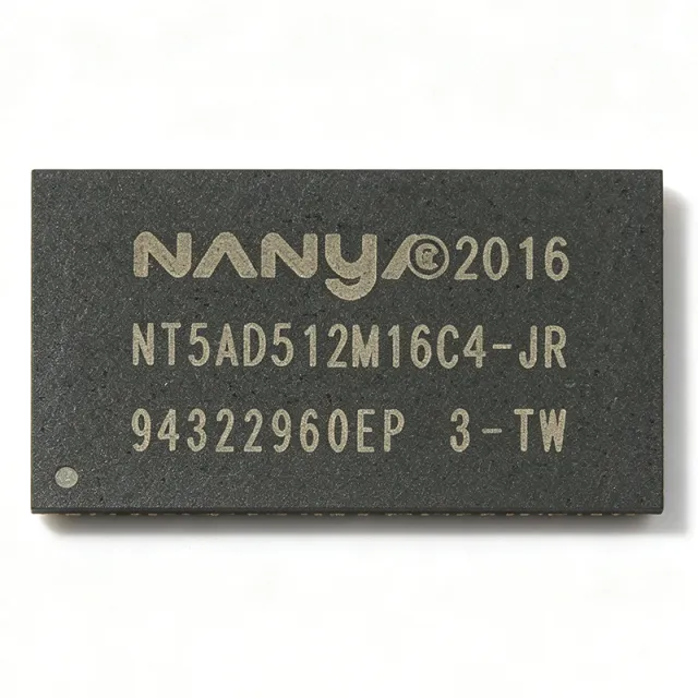
NT5AD512M16C4-JRU - DDR4 8Gb 512Mx16 Industrial SDRAM | Nanya
The Nanya Technology NT5AD512M16C4-JRU is an 8 Gbit DDR4 SDRAM organized as 512M x 16, operating at 1600 MHz (3200 Mbps data rate) with CL22 latency, powered from a 1.2 V VDD supply and housed in a 96-ball FBGA (PBGA96) surface-mount package. The U suffix denotes the industrial temperature grade of -40 C to +95 C with auto self-refresh support. DDR4 SDRAM (Double Data Rate 4 Synchronous Dynamic Random Access Memory) is the fourth generation of DDR DRAM, a class of volatile memory that stores each bit in a capacitor-based cell and transfers data on both clock edges. Within the memory hierarchy, DDR4 sits in the main-memory tier between cache SRAM and storage, and functions as the primary working memory for CPUs, MPUs, FPGAs, and ASICs in embedded and enterprise systems. Key features include auto self-refresh with a built-in temperature sensor, auto precharge, asynchronous reset, data mask (DM), write leveling, dynamic on-chip termination (ODT), ZQ calibration, and CRC functions. These capabilities reduce controller burden and improve signal integrity at high data rates, making the device reliable in wide-temperature industrial environments. Technically, the NT5AD512M16C4-JRU uses a CMOS core with a bank-group architecture supporting burst, interleaved, and 8n prefetch operations. The 16-bit I/O width simplifies 32-bit and 64-bit bus designs by reducing the number of components per bus compared with x4/x8 parts. Speed bins from 800 Mbps up to 3200 Mbps are supported across the JR family, with CL values scaling from CL12 to CL22 per the frequency table in the Nanya DDR4 8Gb datasheet. Typical applications include industrial automation controllers, networking and communication equipment, smart IoT gateways, office and enterprise systems, and automotive-adjacent industrial platforms where -40 C to +95 C operation is mandatory. When designing with this component, follow JEDEC DDR4 routing practice for length matching, ODT settings, and ZQ resistor placement, and verify controller compatibility with the 512M x16 organization and industrial speed bin. This page synthesizes distributor pricing, drop-in alternatives from Nanya and cross-brand sources, and practical design notes not found in the manufacturer datasheet.

PDRQLAKCDF12-00 - 16Gb DDR5-7200 SDRAM | Samsung Electronics
The Samsung Electronics PDRQLAKCDF12-00 is a 16 Gbit DDR5 SDRAM DRAM component organized as 1G x 16, operating at DDR5-7200 data rates (7200 Mbps/pin) at the JEDEC-standard 1.1 V operating voltage, packaged in a 102-ball FBGA surface-mount package. A DRAM (Dynamic Random Access Memory) is the primary volatile working memory in modern computing systems, sitting at the top of the memory hierarchy below CPU caches. DDR5 SDRAM is the fifth generation of double-data-rate synchronous DRAM, doubling the bank groups and burst length of DDR4, moving the power management IC (PMIC) onto the module, and lowering the per-bit operating voltage to 1.1 V for improved power efficiency in high-density memory subsystems. Key features of the PDRQLAKCDF12-00 include its 7200 Mbps data rate - an improvement over the previous 6400 Mbps DDR5 generation - a 1G x16 organization suited to wide-memory-bus designs, and the JEDEC-standard 1.1 V operating voltage with on-die termination and on-die ECC features typical of the DDR5 generation. The 102-ball FBGA (fine-pitch ball grid array) package provides a compact surface-mount footprint for direct mounting on memory modules or on-board memory designs. Architecturally, this device belongs to Samsung's DDR5 DRAM component family. Samsung has sampled native 7200 Mbps DDR5 products in two packages: the 78-ball FBGA PDRQL8KCBF12-00 and the 102-ball FBGA PDRQLAKCDF12-00, both supporting 7200 Mbps at 1.1 V per JEDEC specification. The x16 organization of this part reduces the number of components needed to populate a 64-bit or 128-bit channel. Typical applications include PC and workstation UDIMM/SO-DIMM memory modules, client and server RDIMM designs, graphics and accelerator board memory, and embedded on-board memory in networking and industrial systems that require high bandwidth. Designers should verify BIOS/memory-controller training support for the 7200 Mbps speed bin, and ensure power delivery follows the DDR5 PMIC architecture at 1.1 V. This page synthesizes distributor availability data, speed-bin context, and drop-in alternative options not found on a single manufacturer page.

W25M512JVEIQ - 512Mbit SPI NOR Flash 104MHz | Winbond
The Winbond W25M512JVEIQ is a 512Mbit (64MB) serial NOR flash multichip package (MCP) memory IC with SPI, Dual SPI and Quad SPI interface support, a maximum clock frequency of 104 MHz, and 3V/3.3V operation, housed in an 8-pin WSON (8mm x 6mm) package with exposed pad. A serial NOR flash memory is a non-volatile storage device that retains code and data without power and is accessed over a simple serial peripheral interface. In the system memory hierarchy, NOR flash occupies the code-storage tier: unlike NAND flash, it offers random-access reads with fast, byte-level access, which makes it the standard boot medium for microcontrollers, processors, and FPGAs. A multichip package (MCP) such as the W25M series stacks multiple die - for example dual NOR or NOR+NAND - inside one package, doubling or tripling density without enlarging the PCB footprint. Key features of the W25M512JVEIQ include 512Mbit capacity organized as 64M x 8, uniform 4KB sectors per the Mouser listing, and Quad SPI operation up to 104 MHz that delivers high read throughput for XIP (execute-in-place) booting. The WSON-8 (8x6) package with exposed pad provides low thermal impedance and a compact footprint suitable for dense boards. The device uses Winbond spiFlash technology with standard JEDEC-recognized SPI command sets (read, page program, sector/block erase), standarddual- and quad-output commands, and hardware write protection via the /WP pin. The MCP architecture integrates stacked die internally so the host sees a single SPI target, simplifying firmware compared with board-level chip stacking. Typical applications include embedded boot code storage for Linux-based SoCs and microcontrollers, FPGA configuration bitstreams, networking and industrial equipment firmware, and set-top-box or display firmware where 64MB of XIP-capable code storage is required. Designers should verify whether their boot ROM supports the W25M MCP command mapping, since the W25M series uses a die-select wrapper distinct from the single-die W25Q family; 10k pull-ups on /HOLD and /WP and a 0.1uF decoupling capacitor close to VCC are standard practice. This page synthesizes distributor pricing, drop-in alternatives, pinout, and practical design notes not found in the manufacturer datasheet, with pricing referenced as of 2026-09-10.
W948D6FBHX5I-TR - 256Mb LPDDR 200MHz DRAM | Winbond
The Winbond Electronics W948D6FBHX5I-TR is a 256Mbit Mobile LPDDR SDRAM memory IC organized as 16M x16, operating at 200 MHz with a 5 ns access time, supplied at 1.8V and housed in a 60-ball VFBGA (8x9 mm) package delivered on tape and reel. Mobile LPDDR SDRAM is a low-power variant of synchronous dynamic random access memory designed for battery-powered and space-constrained systems. Within the memory hierarchy, DRAM sits as fast volatile working memory below SRAM in access latency but far above it in density, making LPDDR the workhorse main-memory technology for portable electronics, embedded processors, and application-specific SoCs. Key features include the 256Mbit density in a x16 organization, a 200 MHz clock rate (CL=3 latency class), a single 1.8V power supply that reduces dynamic and standby power versus standard 2.5V SDRAM, and the compact 60-ball VFBGA footprint of only 8x9 mm that minimizes PCB area. The I suffix grade supports industrial temperature ranges, and partial-array self-refresh options lower retention current in sleep modes. Architecturally, the device uses a double-data-rate-style interface with differential clocking, four internal banks, and programmable burst lengths, following Winbond's W948D6 Mobile LPDDR family design. Power-saving modes such as power-down and deep power-down allow aggressive energy management in duty-cycled systems. Typical applications include portable media players, GPS and navigation devices, industrial HMI panels, embedded Linux/RTOS main memory, and battery-powered data loggers where low standby current matters. Design consideration: ensure the memory controller supports LPDDR (mobile SDRAM) timing registers, and route the 1.8V rail with clean decoupling since BGA ball access restricts post-layout rework. This page consolidates distributor pricing, drop-in family alternatives, and practical design notes beyond what the manufacturer datasheet alone provides.

W971GG6NB-25 TR - 1Gbit DDR2 SDRAM 400MHz | Winbond
The Winbond Electronics W971GG6NB-25 TR is a 1 Gbit DDR2 SDRAM memory IC organized as 64M x 16 (8,388,608 words x 8 banks x 16 bits), operating at a 400 MHz clock rate with 57.5 ns access time, housed in an 84-ball TFBGA package (8 x 12.5 mm) supplied in Tape & Reel packaging. DDR2 SDRAM (Double Data Rate Type Two Synchronous Dynamic Random Access Memory) is a class of volatile memory that transfers data on both rising and falling edges of the clock, doubling effective bandwidth compared to single data rate SDRAM. Within the memory hierarchy, it sits as a main-system-memory technology between DDR1 and DDR3, and remains widely used in cost-sensitive embedded and industrial designs that do not require DDR3/DDR4 bandwidth. Key features include a JEDEC-compliant SSTL_18 interface operating from a single 1.8V supply, 8 internal banks with burst lengths of 4 or 8, and on-die termination support. The x16 organization simplifies 16-bit and 32-bit memory subsystems by reducing required bus width and controller complexity. Architecturally, the device achieves high-speed transfer rates up to DDR2-800 class performance, using a 4n prefetch architecture that internally runs at half the external data rate. Posted CAS additive latency and programmable CAS latency help the memory controller schedule reads efficiently and minimize command bus contention. Typical applications include set-top boxes, networking equipment, industrial HMI panels, digital television, and embedded processor memory subsystems for SoCs requiring DDR2 interfaces. Design consideration: ensure SSTL_18 signal integrity with proper on-die or external termination and adhere to datasheet trace-length matching rules for the 84-TFBGA ballout; refresh (64 ms) must be scheduled per controller settings. This page synthesizes distributor pricing, drop-in family alternatives, and practical DDR2 design notes not consolidated in the manufacturer datasheet.
W9751G6NB-25-TR - 512Mb DDR2-800 SDRAM x16 | Winbond
The Winbond Electronics W9751G6NB-25-TR is a 512 Mbit DDR2 SDRAM memory IC organized as 32M x 16 (8M words x 4 banks x 16 bits), operating at a 400 MHz clock rate (DDR2-800 data rate) with a random access time of 57.5 ns, supplied in an 84-ball VFBGA package measuring 8 x 12.5 mm. DDR2 SDRAM (Double Data Rate 2 Synchronous Dynamic Random Access Memory) is a generation of JEDEC-standard DRAM that transfers data on both clock edges, doubling the effective bandwidth of the predecessor DDR1 while operating from a lower 1.8 V power rail. Within the memory hierarchy, DDR2 SDRAM sits between DDR1 and DDR3 in the dynamic random-access memory (DRAM) family, and remains a cost-effective choice for embedded systems, set-top boxes, and networking equipment whose processors support only DDR2 interfaces. Key features of the W9751G6NB-25 include the -25 speed grade supporting DDR2-800 operation, a posted CAS with additive latency and auto precharge function, a data mask (DM) function for byte-level write masking, and dynamic on-chip termination (ODT) that improves signal integrity at high data rates by terminating the bus inside the chip. The x16 organization suits systems with narrow 16-bit memory buses or dual-chip 32-bit configurations. The device uses a standard DDR2 architecture with a 1.8 V nominal supply, differential strobes (DQS, /DQS) for data capture, and burst lengths of 4 or 8 with interleaved or sequential burst ordering. Refresh and self-refresh modes support low-power standby operation between accesses. Typical applications include set-top boxes, digital TVs, network routers and switches, industrial HMI terminals, and printer or multimedia SoC platforms that specify a 512 Mbit x16 DDR2 memory. Design-wise, pay attention to DDR2 fly-by clock routing, dynamic ODT settings in the memory controller, and address/command bus termination to meet timing at 400 MHz. This page synthesizes distributor pricing from LCSC, DigiKey, and Mouser, drop-in family alternatives, and practical design notes not found in the manufacturer datasheet.