EEPROM
Товары (44)

27C256-12/L - 256Kbit 120ns CMOS EPROM PLCC-32 | Microchip
The Microchip Technology 27C256-12/L is a 262,144-bit (32K x 8) CMOS EPROM with a 120 ns maximum access time, a 4.5V to 5.5V supply range, and a 32-pin PLCC (PQCC32) J-bend surface-mount package. An EPROM (Erasable Programmable Read-Only Memory) is a non-volatile semiconductor memory that is programmed electrically and erased by exposure to ultraviolet light through a quartz window. Within the memory hierarchy, it belongs to the broader category of read-only memory, sitting between masked ROM and electrically erasable EEPROM/Flash devices. EPROMs such as the 27C256 became the de facto industry standard for firmware storage in embedded systems. Key features include CMOS technology for low power consumption, with 20 mA typical active current and 100 uA standby current, and 90 ns access time available in the faster speed grades of the family. The asynchronous architecture requires no clock, and auto-ID support aids automated programming equipment. Factory programming is also available from Microchip. The device uses a standard 27-series pinout compatible with the industry-standard 27256 JEDEC footprint, making it interchangeable with 27C256 devices from multiple manufacturers. The J-bend PLCC package provides reliable surface mounting, improved board-level vibration resistance, and a smaller footprint than DIP equivalents. Typical applications include legacy firmware storage in industrial controllers, embedded boot code in telecommunications equipment, automotive ECUs, and replacement ROMs for vintage computer and test-equipment repair. A key design consideration is that this part is discontinued by Microchip; for new designs, electrically erasable alternatives such as the AT28C256 EEPROM or 29C-series Flash should be evaluated, noting pin 1 and pin 27 functional differences between EPROM and EEPROM pinouts. This page synthesizes distributor availability data, drop-in alternatives, and practical design notes not found in the manufacturer datasheet.

27C256L-20R - 256Kbit 32Kx8 CMOS EPROM 200ns | WSI
The WSI 27C256L-20R is a 256 Kilobit (32K x 8-bit) CMOS EPROM with a 200 ns access time, housed in a 28-pin package with JEDEC-approved pinout. The 27C256L-20R operates from a single +5 V power supply with a standard +/-10% supply tolerance. An EPROM (Erasable Programmable Read-Only Memory) is a non-volatile semiconductor memory device that retains programmed data without power. Data is written electrically at programming time and can be erased only by exposure to ultraviolet light through the quartz window of the ceramic package. EPROMs sit in the memory hierarchy between mask ROM (fixed at fabrication) and EEPROM/Flash (electrically erasable), and are classified as Memory ICs within the broader integrated circuit family. Key features of the 27C256 family include fast access-time speed options (as fast as 150 ns on faster grades; the -20 suffix denotes 200 ns), very low power consumption with 20 uA typical CMOS standby current on the L (low-power) variant, a JEDEC-approved 28-pin pinout, and single +5 V operation. The 100% Flashrite programming scheme allows typical programming times per byte to be minimized, speeding production programming throughput. Architecturally, the device organizes 262,144 bits as 32,768 words of 8 bits each, addressed via 15 address lines (A0-A14) with eight bidirectional data lines (O0-O7). Control is provided by chip enable (CE), output enable (OE), and program (PGM/VPP) pins, allowing standard memory-bus interfacing and read operation with CMOS-level standby currents when deselected. Typical applications include firmware and BIOS storage in legacy embedded systems, industrial control boards, automotive ECUs of the pre-Flash era, telecom equipment, and replacement/repair of obsolete ROM devices in service and maintenance scenarios. When designing with this EPROM, respect the 200 ns access time when matching to microprocessor wait-state requirements, and provide proper VPP/PGM handling during in-system or off-board programming. Note that erasure requires a UV eraser, not electrical erasure. This page synthesizes distributor pricing, drop-in alternatives, and practical design notes not found in the manufacturer datasheet.

27C256T-15/SO - 256K 32Kx8 CMOS EPROM 150ns | Microchip Technology
The Microchip Technology 27C256T-15/SO is a 256Kbit (32K x 8) CMOS UV-erasable EPROM with a maximum access time of 150 ns, operating from a 4.5V to 5.5V supply in a 28-lead SOIC surface-mount package. It is a one-time-programmable-class parallel memory device in the industry-standard 27C256 family footprint. An EPROM (Erasable Programmable Read-Only Memory) is a non-volatile semiconductor memory that retains firmware or fixed data without power and can be erased with ultraviolet light when housed in a quartz-window package; the plastic SOIC variant is intended for one-time programming in production. Within the memory hierarchy it sits under Memory ICs, in the broader category of non-volatile parallel memory alongside EEPROM and flash, and remains common in legacy and industrial systems. Key features include CMOS technology for low power consumption with 20 mA active current and 100 uA standby current, 150 ns maximum access time for asynchronous parallel interfacing, 3-state outputs, and Auto ID identification to aid automated programming equipment. Factory programming and auto-insertion-compatible plastic packages are supported. The device uses CMOS process technology to achieve a low standby current of 100 uA, which is valuable in battery-backed or power-sensitive legacy designs. Access is fully asynchronous with /CE, /OE, and PGM control lines, and the 3-state outputs allow direct bus connection in microprocessor systems. Typical applications include legacy firmware storage in industrial controllers, automotive ECUs and engine-management ROM sockets, telecommunications equipment, and retro-computing repair where a 27C256 socket must be populated with a surface-mount device. Design consideration: since this is an EPROM, the programmed content cannot be electrically erased; verify firmware on a programmer before soldering, and respect the 4.5V to 5.5V VCC window and programming voltage requirements on VPP. This page synthesizes distributor availability data, drop-in alternatives, and practical design notes not consolidated in the manufacturer datasheet. Pricing references are as of 2026-09-13.
27C512-15FA - 512Kbit CMOS UV EPROM 150ns CDIP-28 | ASI
The ASI 27C512-15FA is a 512-Kbit (65,536 x 8-bit) CMOS UV-erasable programmable read-only memory (UVPROM/EPROM) with a 150 ns access time, housed in a 28-pin ceramic DIP (CDIP-28) package with a quartz erase window. According to the manufacturer and distributor listings, the device is a non-volatile memory organized as 64K x 8 bits and is offered in commercial temperature grade. An EPROM (Erasable Programmable Read-Only Memory) is a non-volatile semiconductor memory that retains programmed data without power and can be erased by exposure to ultraviolet light through a quartz window in the ceramic package. EPROMs sit in the memory hierarchy alongside ROM, EEPROM and flash memory, and the 27C512 family was the de facto industry standard 512-Kbit UV EPROM used across microprocessor-based systems from the 1980s through today's legacy designs. Key features of the 27C512-15FA include the 150 ns access time (suffix -15), which supports zero-wait-state operation of mid-speed microprocessors; the ceramic DIP-28 package with UV erase window, allowing thousands of erase/program cycles in development workflows; CMOS technology for low static power consumption; and a standard 28-pin JEDEC-style pinout shared across the 27x512 family from multiple manufacturers. The CMOS process keeps standby current low and provides wide noise margins, while the 5 V-typical operating environment of the era simplifies integration into classic bus architectures. Programming is performed at elevated VPP levels through the standard 27C512 programming algorithm on compatible device programmers. Typical applications include firmware and BIOS storage in legacy industrial equipment, arcade game cartridges and retro-computer boards, telecommunications line cards, test instrumentation, and replacement/repair spares for systems that were designed around UV EPROMs and cannot easily migrate to flash memory. A key design consideration is that once the quartz window is covered after final programming, the device behaves like a one-time-programmable ROM in the field; UV erasure requires a standard EPROM eraser with the specified UV dose, and the window must be kept covered to prevent accidental data loss from sunlight or fluorescent light. This page synthesizes distributor pricing, drop-in alternatives from multiple manufacturers, pinout data, and practical design notes not consolidated in any single manufacturer datasheet.

27C512MC-15 - 512Kbit CMOS EPROM 150ns | MX | Embedded Systems
The MX 27C512MC-15 is a 512 Kbit (64K x 8) CMOS UV-erasable/OTP EPROM with a 150 ns access time, single +5V power supply operation, and a +12.5V programming voltage, housed in a surface-mount/through-hole 27C512-standard 28-pin package. An EPROM (Erasable Programmable Read-Only Memory) is a non-volatile memory IC that retains firmware without power. It belongs to the memory IC family hierarchy: EPROM -> non-volatile memory -> semiconductor memory -> integrated circuit. UV versions erase through a quartz window under UV light; OTP (one-time-programmable) versions ship without the window at lower cost. EPROMs remain essential for legacy embedded system maintenance, retro-computing, ECU reprogramming, and industrial equipment firmware updates where flash replacements cannot meet timing or pinout constraints. Key features include the 64K x 8 organization, a fast 150 ns access time in the -15 speed grade, completely static operation requiring no clocks or refresh, and full TTL compatibility on inputs and outputs. The family also offers 45/55/70/90/100/120/150 ns speed grades, giving designers timing headroom across the range. Single +5V read operation simplifies power design, while programming uses +12.5V VPP. Technically, the 27C512 uses CMOS process technology for low power consumption with standby current far below bipolar predecessors. Address inputs A0-A15 select one of 65,536 byte locations; active-low CE and OE controls gate the tri-state outputs, allowing multiple devices to share a data bus. In a microprocessor system, the 150 ns access time supports faster bus cycles than the common 200-250 ns legacy parts, provided address setup timing is respected. Typical applications include arcade game board and retro-computer ROM replacement, automotive ECU calibration chips, industrial PLC firmware storage, and telecom equipment boot code where JEDEC 28-pin EPROM footprints must be preserved. Design consideration: verify the CE-to-output access time (tCE) as well as address access time, and ensure programming equipment supports the +12.5V VPP specification of this CMOS family. This page synthesizes distributor data, drop-in alternatives, and practical design notes not found in the manufacturer datasheet.

CY14B101KA-SP45XI - 1Mbit nvSRAM 45ns with RTC | Infineon
The Infineon (Cypress) CY14B101KA-SP45XI is a 1-Mbit (128K x 8) nonvolatile SRAM (nvSRAM) memory IC with a full-featured real-time clock, offering 45 ns parallel access time, 3V operation, and a 48-pin SSOP surface-mount package with industrial temperature grading. An nvSRAM (nonvolatile static RAM) is a memory device that combines the fast, unlimited read/write endurance of conventional SRAM with the nonvolatility of EEPROM or Flash. In the memory hierarchy, it sits above standard SRAM (which loses data at power-off) and below battery-backed SRAM solutions (which require cells and maintenance), making it part of the broader nonvolatile semiconductor memory family alongside FRAM, MRAM, and Flash. Key features include QuantumTrap nonvolatile element technology, which Infineon describes as producing the world's most reliable nonvolatile memory; infinite SRAM read and write cycles; independent nonvolatile storage that resides in quantum trap cells; and an integrated real-time clock in the same monolithic IC, eliminating a separate RTC chip and its battery-backup circuitry in many designs. Technically, the device operates as standard asynchronous SRAM until a store operation transfers SRAM contents into the nonvolatile elements, either automatically (on power loss) or under software/hardware control. A recall operation restores data from the nonvolatile elements back to SRAM at power-up. The 45 ns access time supports zero-wait-state operation with many microprocessors and FPGAs on a parallel address/data bus. Typical applications include industrial data loggers, PLCs and factory automation equipment, metering systems requiring event and time stamping via the RTC, and networking or telecom equipment storing configuration and event data that must survive abrupt power failures. Design consideration: budget the nonvolatile store cycle time (tSTORE) into your system timing, since the device is busy during a store operation, and ensure the power supply supervisor triggers auto-store before VDD falls below the minimum level. This page synthesizes distributor pricing, drop-in alternative analysis, and practical design notes not found in the manufacturer datasheet, with all specifications traceable to the Infineon/Cypress datasheet and distributor listings as of 2026-09-13.

CY14V104LA-BA45XIT - 4Mb nvSRAM 45ns 3.3V | Infineon | Industrial
The Infineon Technologies CY14V104LA-BA45XIT is a 4 Mbit non-volatile SRAM (nvSRAM) memory IC with a 45 ns access time, a 3.0 V to 3.6 V power supply range, and a 512K x 8 parallel SRAM interface, housed in a 48-ball FBGA (6 x 10 mm) package. An nvSRAM (non-volatile SRAM) is a memory device that combines the unlimited read/write endurance and fast access of standard static RAM with non-volatile data storage. In the memory hierarchy, nvSRAM sits alongside EEPROM and Flash as a non-volatile memory IC, but unlike EEPROM it offers SRAM-speed reads and writes on every access. In the CY14V104LA family, the non-volatile element is a SONOS-based quantum-trap storage cell, and data is automatically stored to the non-volatile array on power loss without any external intervention. Key features of the CY14V104LA include 45 ns random access timing suitable for zero-wait-state parallel buses, unlimited SRAM read/write endurance, and automatic non-volatile STORE operations on power-down plus automatic RECALL on power-up. The device supports hardware STORE via an external pin and software-initiated stores, with data retained in the non-volatile cells for a long archival period specified in the manufacturer datasheet. Technically, the device reads and writes like a standard asynchronous SRAM while internally managing charge and data transfer to the SONOS non-volatile elements. Because storage occurs automatically during power fail detection, no external supervisory circuitry or battery is required - a key advantage over battery-backed SRAM solutions. Typical applications include industrial PLC data logging, network router configuration storage, metering and e-meter data retention, aerospace and avionics black-box buffers, and robotics control tables where frequent high-speed writes and instant power-fail retention are both required. Design consideration: budget for the STORE cycle time after a hardware or software STORE command; the device becomes unavailable during non-volatile storage, so system firmware should sequence writes accordingly. This page synthesizes distributor pricing, drop-in same-family alternatives, and practical design notes not found in the manufacturer datasheet.

EPCQ16ASI8N - 16Mb Serial Config Device SOIC-8 | Altera (Intel)
The Intel (Altera) EPCQ16ASI8N is a 16Mb in-system-programmable serial configuration device designed to store FPGA bitstreams, operating at 3.3V in an 8-pin SOIC package. A serial configuration device is a non-volatile flash memory optimized specifically for loading configuration data into an FPGA at power-up. In the memory IC hierarchy, it belongs to configuration PROMs for FPGAs, a subset of serial NOR flash memory. The FPGA includes dedicated logic that reads the bitstream from the EPCQ device over a serial interface (active serial or passive serial modes) during every power cycle, so the configuration memory is a mission-critical element of any standalone FPGA system. The EPCQ16ASI8N offers 16 Mbit of capacity, sufficient for mid-range Intel/Altera FPGAs and CPLDs. It supports fast read operations including quad-serial data modes, which minimize boot times by transferring four bits per DCLK cycle. In-system programmability (ISP) allows the device to be reprogrammed via a JTAG-to-configuration chain using tools such as Intel Quartus Prime without removing the part from the board. The device operates from a single 3.3V supply, keeping power-rail design simple. Architecturally, the EPCQ-A family uses standard serial NOR flash commands, and its state machine is optimized for FPGA load sequencing, including proper power-on-to-first-read behavior. The industrial temperature version (I suffix) supports -40C to +85C operation, suiting harsh-environment deployments. Typical applications include bitstream storage for Intel Cyclone and MAX series devices, remote FPGA field upgrades, industrial control, and communications equipment where the FPGA must load autonomously at power-up. Design tip: verify that your FPGA's configuration mode (e.g., Active Serial x1 or Fast x4) and the maximum supported EPCQ density match the 16Mb device before layout. Pull NCONFIG and NSTATUS appropriately and keep DCLK traces short. This page adds distributor pricing, drop-in alternatives, comparison tables, and practical design notes beyond the manufacturer datasheet.
HMAA8GR7CJR4N-RD - 64GB DDR4-3200 ECC RDIMM | SK hynix
The SK hynix HMAA8GR7CJR4N-RD is a 64GB DDR4 registered DIMM (RDIMM) with ECC, operating at 3200 MT/s (PC4-25600) at 1.2V in a 288-pin dual-rank (2Rx4) form factor. A registered DIMM (RDIMM) is a server-class memory module that buffers the command and address signals through a register IC before they reach the DRAM chips, reducing electrical loading on the memory controller and enabling higher module counts per channel than unbuffered UDIMMs. Within the memory hierarchy, RDIMMs belong to the DDR4 SDRAM family, itself part of the broader volatile dynamic random access memory (DRAM) category used in servers, workstations, and data-center platforms. Error-correcting code (ECC) adds extra check bits (x4/x72 organization) so single-bit memory errors can be detected and corrected in flight, which is essential for uptime-critical computing. Key features of the HMAA8GR7CJR4N family include 64GB capacity organized as 8Gx72, dual rank (2Rx4) with 36 4Gb x4 Flipchip SDP DDR4 components, 3200 Mbps transfer rate (PC4-25600), and 1.2V operation for reduced power compared with DDR3. The -RD suffix in this MPN denotes the module speed-temperature grade configuration of the 16Gb C-die based RDIMM family (HMAA8GR7CJR4N / HMAA4GR7CJR8N / HMAA4GR7CJR4N), per the SK hynix 16Gb C-die RDIMM datasheet. Architecturally, the module uses 16Gb C-die (CJR) DDR4 components mounted on a 288-pin registered ECC DIMM PCB with a register and SPD hub. The x4 DRAM device width, combined with ECC, enables Chipkill-class reliability when paired with server memory controllers. CL22 timing at 3200 MT/s provides a first-word latency of approximately 13.75 ns, balancing bandwidth and latency for virtualization workloads. Typical applications include enterprise servers (Dell PowerEdge, HPE ProLiant, Lenovo ThinkSystem), virtualization hosts, and data-center compute nodes that require high-density, ECC-protected memory at DDR4-3200 speeds. Design consideration: verify that your server platform supports DDR4-3200 RDIMMs and populate memory channels symmetrically (same module type per channel) to maximize bandwidth; mixing module grades can force derating to lower speeds. This page synthesizes distributor stock data, drop-in alternatives, and practical deployment notes not found in the manufacturer datasheet.
HMCG84AHBRA290N - 32GB DDR5-6400 ECC RDIMM | SK Hynix
The SK Hynix HMCG84AHBRA290N is a 32GB DDR5-6400 ECC Registered DIMM (RDIMM) operating at 6400 MT/s (PC5-51200), CAS Latency 52, at 1.1V, in a 288-pin DIMM form factor. This single-rank x4 module targets enterprise servers, edge compute nodes, and general-purpose data center hosts. A Registered DIMM (RDIMM) is a type of server memory module that buffers the address and command signals through a register chip, reducing the electrical load on the memory controller and allowing more modules per channel than unbuffered UDIMMs. Within the memory hierarchy, RDIMM sits between LRDIMM (which buffers data too) and UDIMM (unbuffered), making it the standard choice for most two-socket server platforms. Key features include DDR5 architecture with on-die ECC and link ECC, a 6400 MT/s data rate yielding up to 51.2 GB/s peak bandwidth per module, and a 1.1V operating voltage that reduces power draw roughly 30% versus DDR4 RDIMMs at comparable bandwidth. The module also integrates a 5-bit SPD hub (PMIC-managed power delivery) per JEDEC DDR5 requirements. The 1Rx4 single-rank x4 organization uses x4 DRAM devices whose inherent ECC assists with high-reliability operation and supports post-package repair in data center service. SK Hynix manufactures both the DRAM dies and the assembled module, ensuring full-stack qualification. Typical applications include AI inference and training nodes, virtualization hosts with low VM density, cloud compute instances, and high-performance database servers requiring validated ECC RDIMM bandwidth. Design consideration: verify your server platform's Qualified Vendor List (QVL), as 6400 MT/s operation often requires 1DPC (one DIMM per channel) population; two DIMMs per channel may downclock to 5600 MT/s. This page synthesizes distributor availability, same-brand drop-in RDIMM alternatives, and platform-selection guidance not consolidated in any single manufacturer page.
HMCG88AEBRA168N - 32GB DDR5 4800 ECC RDIMM | SK hynix
The SK hynix HMCG88AEBRA168N is a 32GB DDR5 ECC Registered DIMM (RDIMM) server memory module operating at 4800 MT/s (PC5-38400 bandwidth) with CL40 latency at 1.1V, housed in a 288-pin DIMM form factor. DDR5 RDIMM (Registered Dual In-line Memory Module) is the enterprise-class memory standard for servers and workstations. Unlike consumer UDIMMs, an RDIMM uses a register to buffer address and command signals, reducing electrical load on the memory controller and enabling higher module counts per channel. DDR5 doubles the number of independent channels per DIMM versus DDR4 (two 32-bit subchannels) and moves the power management IC (PMIC) onto the module, improving signal integrity and power efficiency at the 1.1V operating voltage. Key features of the HMCG88AEBRA168N include 32GB capacity in a dual-rank x8 organization, ECC (Error Correcting Code) for detecting and correcting single-bit memory errors that could otherwise crash a server, 4800 MT/s data rate conforming to the PC5-38400 DDR5 speed grade, and CL40 CAS latency. The 1.1V standard DDR5 voltage keeps power draw and thermal output low in dense chassis. The registered architecture and on-die ECC make this module suited to data-intensive workloads where uptime matters: virtualization hosts, database servers, and high-memory-density blade systems. Dual-rank organization improves effective bandwidth through interleaving in many server workloads. Typical applications include enterprise rack servers, hyper-converged infrastructure, cloud compute nodes, and workstation memory upgrades requiring validated ECC RDIMMs. Design and procurement consideration: always verify that the target server platform (CPU and BIOS) supports DDR5-4800 RDIMMs and the installed rank count per channel, as population rules affect achievable speed. Note that RDIMMs are not interchangeable with consumer UDIMMs or LRDIMMs. This page consolidates distributor pricing, cross-referenced drop-in alternatives, and practical deployment notes not found in a single manufacturer listing, so engineers and IT buyers can validate compatibility in one place.
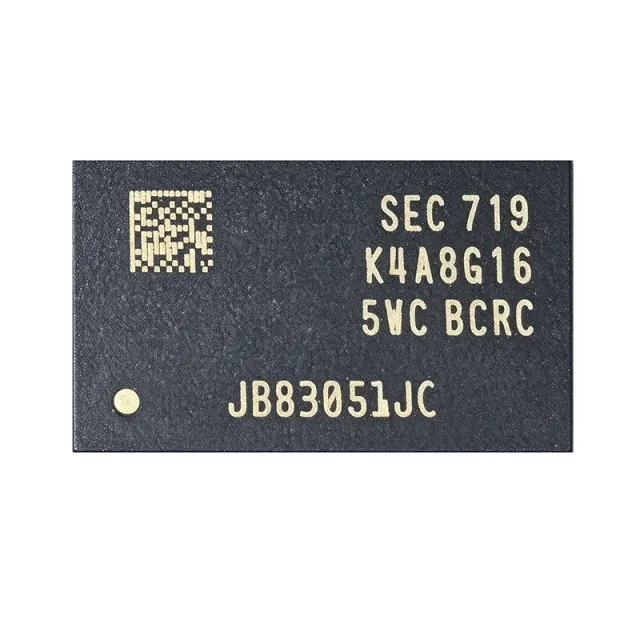
K4A8G165WC-BCRC - 8Gb DDR4 SDRAM 2400Mbps x16 | Samsung
The Samsung K4A8G165WC-BCRC is an 8 Gb DDR4 SDRAM memory IC organized as 512M x 16, operating at a data rate of 2400 Mbps (1333 MHz clock) from a nominal 1.2 V supply (1.14 V to 1.26 V), housed in a 96-ball FBGA (TFBGA) package. DDR4 SDRAM (Double Data Rate 4 Synchronous Dynamic Random Access Memory) is the fourth generation of the JEDEC-defined DDR memory family. In the system hierarchy it sits under synchronous DRAM -> volatile memory IC -> semiconductor memory, serving as the main working memory for processors, SoCs and controllers. DDR4 lowered operating voltage from DDR3's 1.5 V to 1.2 V, cutting dynamic power by roughly 25% while raising data rates up to 3200 Mbps. Key features of this C-die part include an 8 Gbit density in a x16 organization with a 16-bit data interface, auto precharge, asynchronous reset, CRC and CA parity for command/address integrity, on-die ZQ calibration, dynamic on-die termination (ODT), and data mask (DM) support per byte lane. These features improve signal integrity and data reliability at high speeds. Technically, the device uses Samsung's C-die process and a bank-group architecture that allows faster burst access between bank groups. Ballouted per JEDEC DDR4 standards, the 96-ball FBGA is the industry-standard footprint, so JEDEC-compliant x16 8 Gb DDR4 parts from other vendors land on the same PCB land pattern. Operating current is specified around 2 mA (standby idle) and up to 64 mA operating per distributor data. Typical applications include embedded computing modules, industrial controllers, networking and gateway equipment, set-top boxes, smart TVs, medical monitoring devices, and test and measurement instruments that need a compact, soldered-down memory. Design tip: route the 16-bit data bus with length-matched traces to the controller, honor VTT termination (dynamic ODT helps), and decouple the 1.2 V VDD rail with low-ESR ceramics close to the ball field; verify speed-grade compatibility with your memory controller's trained timings. This page synthesizes distributor pricing, verified drop-in alternatives, design notes and FAQs not consolidated in the manufacturer datasheet.
K9ADGD8S0A - 3D V-NAND TCAT Flash Memory Die | Samsung
The Samsung K9ADGD8S0A is a bare-die 3D vertical NAND (V-NAND) flash memory device manufactured using Samsung's proprietary terabit cell array transistor (TCAT) technology. According to TechInsights structural analysis (report SAR-1407-802), this die was found inside Samsung K9HQGY8S5M-CCK0 and K9LPGY8S1M-CCK0 V-NAND packages extracted from the Samsung 850 Pro 128 GB SSD. V-NAND flash is a category of non-volatile memory in which memory cells are stacked vertically rather than arranged in a planar 2D layout. As a member of the NAND flash hierarchy (NAND flash -> flash memory -> non-volatile semiconductor memory -> solid-state storage), V-NAND overcomes the scaling limits of planar NAND by increasing bit density vertically. The TCAT process builds the channel vertically through stacked conductive layers, enabling high endurance and stable cell characteristics. Key characteristics of the K9ADGD8S0A die include its 3D V-NAND architecture, TCAT fabrication process, and role as a component-level building block inside packaged V-NAND products. Because it is sold as a bare die rather than a packaged component, it is primarily of interest for structural analysis, failure analysis, reverse engineering, research, and educational purposes rather than standard PCB assembly. Typical use cases include semiconductor process analysis, competitive teardown studies, material science research on charge-trap flash cells, and academic study of 3D NAND architectures. TechInsights and REATISS have both published structural and process analyses of this exact die. Design consideration: this part is not a drop-in component for PCB designs; it is a die-level product with no publicly available commercial datasheet, pinout, or pricing from authorized distributors. This page synthesizes verified teardown analysis data, related V-NAND family members, and sourcing context not found in standard distributor listings.
K9FGGY8J5A-CCK0 - Samsung NAND Flash Memory | SSD Storage
The Samsung K9FGGY8J5A-CCK0 is a high-density raw NAND flash memory component manufactured by Samsung Electronics, belonging to the K9F/K9G family of managed-raw NAND devices used as storage media in solid-state drives, embedded storage modules, and industrial memory applications. Samsung codes the part number to encode generation, density, organization, and package: the CCK0 suffix denotes a specific speed grade and lead-free/RoHS-compliant packing option within the same silicon family. NAND flash is a non-volatile memory technology in which memory cells are connected in series, allowing the highest bit density per silicon area of any mainstream memory type. Within the memory hierarchy, NAND flash sits below volatile DRAM in speed but provides persistent storage at far lower cost per gigabyte, making it the foundation of SSDs, eMMC storage, USB drives, and memory cards. NAND devices are hierarchical: cells form pages, pages form blocks, and blocks form planes; data is read and programmed at page granularity and erased at block granularity. Key characteristics of Samsung K9-family high-density NAND include multi-level or triple-level cell storage for maximum bit density, an asynchronous or_toggle-mode I/O interface for command/address/data transfer, on-die charge-pump circuitry for program and erase voltages, and array of status, ID, and feature registers accessible through standard NAND command sets. Exact density, organization, page size, block size, and interface speed parameters for this specific ordering code must be confirmed against the official Samsung datasheet before design-in. Technically, K9-series devices use a command/address/data multiplexed 8-bit or 16-bit bus with CLE, ALE, WE, RE, CE and R/B control signals, standard Samsung-ONFI compatible command protocols, and internal ECC requirements defined by the cell technology generation. As NAND geometries shrink, host-side ECC strength requirements increase, so controller selection is coupled to the NAND generation. Typical applications include solid-state drive media, embedded storage for industrial controllers, set-top boxes, networking equipment, and high-volume consumer electronics where raw NAND is managed by an external controller. Design consideration: raw NAND requires a memory controller with ECC, wear-leveling, and bad-block management; verify the exact die configuration and speed grade in the Samsung datasheet and confirm controller compatibility before committing a PCB layout. This page synthesizes distributor availability signals, same-family drop-in candidates from the K9 family ordering-code system, and practical design notes not consolidated in the manufacturer datasheet, providing engineers with a single reference point for sourcing and substitution decisions.
K9IUGY8J7B-CCK0 - 1Tb 3D V-NAND TLC Flash | Samsung
The Samsung K9IUGY8J7B-CCK0 is a 1 Terabit (128 GB) 3D V-NAND TLC (triple-level cell) NAND flash memory device built on Samsung's 128-layer, 6th-generation V-NAND technology, supplied in a fine-pitch BGA surface-mount package. It is a raw, non-managed NAND component intended for integration into SSD controllers, eMMC/UFS firmware stacks, and embedded storage systems. Background: NAND flash is a non-volatile memory technology that retains data without power. Within the memory hierarchy, NAND sits below DRAM as mass-storage media; 3D V-NAND stacks memory cells vertically instead of shrinking cells laterally, improving density and endurance. TLC stores 3 bits per cell, tripling density per wafer versus SLC and roughly 1.5x versus MLC, at the cost of tighter program/erase margins that require ECC and controller firmware support. Key characteristics: the 1Tb density in a single monolithic die allows compact PCB area and reduced component count in high-capacity designs. The 3-bits-per-cell TLC architecture paired with 128-layer V-NAND process offers competitive bits-per-programming throughput, and the industrial 'CC' grade suffix denotes Samsung's commercial operating temperature range qualification. Devices of this generation use an ONFI-style asynchronous/synchronous toggle interface - exact timing parameters should be taken from the official Samsung datasheet. Technical depth: V-NAND generation 6 (4448-128L per Samsung internal data for the family) uses charge-trap flash cells with cell strings connected through vertical channels. Page organization, block sizes, and program/erase cycle ratings are die-internal details specified in the vendor datasheet and must not be assumed from prior generations. Typical applications: client and enterprise SSDs, eMMC/UFS-based embedded storage, set-top boxes, networking appliances, and automotive infotainment mass storage (subject to temperature grade verification). Design consideration: TLC NAND requires a controller with strong LDPC ECC, wear leveling, and bad-block management; raw NAND of this class is unsuitable for designs lacking such firmware support. This page synthesizes family cross-references, drop-in same-family alternatives, and practical integration notes not found in the raw datasheet.
K9PDG08U5M - 4Gb x8 SLC NAND Flash 3.3V | Samsung Electronics
The Samsung K9PDG08U5M is a 4Gbit x8-bit organization SLC NAND flash memory device with a 3.3V power supply, housed in a 48-pin TSOP1 surface-mount package. It is part of Samsung's K9P series monolithic NAND flash family designed for mass-storage applications. NAND flash is a type of non-volatile memory that stores data in memory cells arranged in series, enabling very high density and low cost per bit compared to NOR flash. Within the memory hierarchy, NAND flash sits in the solid-state storage class, bridging volatile DRAM and permanent system firmware. It is accessed over an asynchronous 8-bit multiplexed address/data bus with command, address latch enable (CLE/ALE) control, making it the dominant storage medium for embedded systems, SSDs, and memory cards. Key characteristics of the K9PDG08U5M include its x8 multiplexed I/O interface, page-based program and block-based erase operation, and a 3.3V (2.7V to 3.6V) supply rail. The device uses the industry-standard NAND command set (00h-10h page program, 00h-30h page read, 60h-44h block erase per common Samsung conventions), simplifying controller design and software reuse across Samsung NAND generations. Architecturally, the device organizes the 4Gbit array into pages and blocks with a spare area per page for ECC data. Because it is SLC (single-level cell), each cell stores one bit, giving higher endurance and faster access than MLC parts of the same family - a key advantage for industrial and code-storage designs. Ready/Busy (R/B) signaling with open-drain output supports polled or interrupt-driven operation. Typical applications include solid-state drives, USB flash drives, memory cards, set-top boxes, industrial data loggers, and embedded boot code storage where reliability and endurance matter. Design consideration: NAND flash requires error correction code (ECC) - implement Hamming or BCH ECC in the host controller and manage bad blocks per Samsung's bad-block management guidelines; the spare area must be reserved for ECC and bad-block markers. This page synthesizes distributor sourcing data, same-family drop-in alternatives, and practical design notes not found in the manufacturer datasheet, with pricing freshness signals as of 2026-09-04.
K9PRGY8S7M-CCK0 - Samsung NAND Flash Memory BGA | Samsung
The Samsung K9PRGY8S7M-CCK0 is a high-density NAND flash memory device from Samsung Electronics, supplied in a ball grid array (BGA) surface-mount package for embedded storage applications. As part of Samsung's K9-family non-volatile memory lineup, this device provides non-volatile data storage for systems that require gigabyte-class capacity in a compact footprint. NAND flash is a type of non-volatile storage technology that retains data without power. Within the memory hierarchy, NAND flash sits above raw storage media and below system-level SSDs and eMMC/UFS modules: a raw NAND device such as the K9PRGY8S7M-CCK0 provides the memory array and interface, while the host controller manages wear leveling, bad-block management, and error correction code (ECC). Raw NAND is used by designers who want full control of the flash translation layer in their own firmware or controller. Verified web data confirms this part is RoHS / lead-free compliant per distributor listings (Worldway), packaged in BGA, and targeted at applications including automotive body electronics and lighting, communications equipment, wireless infrastructure, personal electronics, and connected peripherals and printers. Samsung NAND family members such as the related K90KGY8S7M-CCK0 (128 GB class) and K9DMGY8J5B-CCK0 share the K9 naming scheme and BGA packaging philosophy. Because this is a raw NAND component, the host system must implement ECC and block management; the exact page size, block size, bus width, supply voltage, and density of the K9PRGY8S7M-CCK0 are not stated in the retrieved web data and must be confirmed from the official Samsung datasheet before design-in. Typical use cases include embedded boards where a dedicated storage controller (for example, an SSD controller such as Samsung's MEX series used in consumer SSDs) manages multiple raw NAND packages. Design consideration: raw NAND requires careful power-rail sequencing, strong ECC (LDPC or BCH depending on the cell type), and thermal management of the BGA solder joints in automotive environments. This page synthesizes distributor listings, family cross-references, and sourcing information for the K9PRGY8S7M-CCK0 not consolidated in any single manufacturer document.

M25P10-AVMN3TP/Y - 1Mbit SPI NOR Flash 50MHz | Micron
The Micron M25P10-AVMN3TP/Y is a 1 Mbit (128 Kbit x 8) serial NOR Flash memory with a 50 MHz SPI-compatible bus interface, operating from a 2.7 V to 3.6 V single supply and housed in an 8-pin SOIC (0.154 in / 208 mil body) package rated from -40C to +125C. A serial NOR Flash memory is a nonvolatile storage IC that stores code and data in a NOR array accessed bit-parallel through a serial peripheral interface (SPI). In the embedded-systems hierarchy it sits under the flash memory family, alongside parallel NOR and NAND Flash, and is typically used as boot code storage for microcontrollers, FPGAs, and system-on-chip devices where a small, low-pin-count, low-cost nonvolatile memory is required. Key features of the M25P10-A include page programming of 1 to 256 bytes with a typical page program time of 1.4 ms, sector erase of 256 Kbit sectors in 0.8 s typical, and a full bulk erase of the 1 Mbit array in 2.5 s typical. The device offers advanced write-protection mechanisms, including block protection and a hardware write-protect (W#) pin, plus a HOLD# pin that suspends serial communication without deselecting the device. Architecturally, the M25P10-A descends from the Numonyx (formerly STMicroelectronics) M25Pxx family, which Micron acquired and continues as part of its low-density serial NOR portfolio. Commands, status registers, and timing follow the industry-standard SPI Flash command set (READ, FAST_READ, PAGE PROGRAM, SECTOR ERASE, BULK ERASE, WREN, RDSR), simplifying driver reuse across designs. Typical applications include MCU boot-code and firmware storage in industrial control, FPGA configuration bitstream storage, set-top boxes, networking line cards, and automotive body modules where the -40C to +125C operating range is required. When designing with this device, keep the SPI clock within the 50 MHz limit for fast read commands and observe proper HOLD# timing to avoid bus contention; add series resistors on MISO if trace lengths are long. This page synthesizes verified distributor data, drop-in alternatives, and practical design notes beyond what the manufacturer datasheet provides.
M25P80-VMN3PB - 8Mbit SPI NOR Flash 75MHz SOIC-8 | Micron
The Micron Technology M25P80-VMN3PB is an 8Mbit (1M x 8) serial NOR flash memory with an SPI bus-compatible serial interface, a maximum clock frequency of 75 MHz, and operation from a 2.7V to 3.6V single supply, housed in an 8-pin SOIC (8-SO) package. Serial NOR flash is a nonvolatile memory category that stores code and data without power and is accessed over a reduced-pin serial interface rather than a parallel bus. Within the memory hierarchy, serial NOR flash sits under NOR flash and memory ICs broadly, and it is the dominant firmware-storage technology for embedded systems because boot code must be directly executable (XIP) from a random-access, byte-addressable nonvolatile array. Key features include 8Mbit density organized as 1M x 8 bits, sector erase (64KB sectors) and bulk erase capability, page programming of up to 256 bytes in 0.64 ms typical, and a 75 MHz maximum SPI clock for fast code shadowing. The standard SPI command set makes the device broadly compatible with MCU QSPI controllers. The M25P80 architecture uses a single die with a serial peripheral interface (SPI) supporting Read, Fast Read, Page Program, Sector Erase, Bulk Erase, and status-register commands. The HOLD and Write-Protect (W) pins allow suspend/resume of serial communication and hardware protection against accidental program or erase operations. Typical applications include firmware/code storage for microcontrollers, FPGA bitstream storage, LCD/display configuration storage, and industrial control systems where reliable nonvolatile code storage is required at low cost. A key design consideration is program/erase endurance: verify erase-before-program sequencing in software and respect sector erase cycle limits for write-intensive logging; for frequent data logging, consider pairing with an EEPROM. This page synthesizes distributor pricing, drop-in alternatives, pinout data, and practical design notes not found in the manufacturer datasheet.

M29F400FT55N3F2 - 4Mbit 5V Parallel NOR Flash 55ns | Micron
The Micron M29F400FT55N3F2 is a 4 Mbit (256K x 16) parallel NOR Flash memory with a 55 ns access time, 5.0 V single supply operation, and a top-boot block architecture, housed in a 44-pin SO (SOP-44) surface-mount package. The F2 suffix denotes Micron's RoHS-compliant, lead-free plating variant, and the T designates top boot block sector mapping. Parallel NOR Flash is a nonvolatile memory technology in which the memory array is addressed over a parallel address bus and read over a parallel data bus, allowing random byte or word access with deterministic, low-latency timing. In the memory hierarchy it sits alongside masked ROM and EEPROM as a code-storage device, and it is the classic choice for storing boot code and firmware because the CPU can execute code directly from it (XIP, execute-in-place) without any controller overhead. Key features of this device include the fast 55 ns access time suitable for zero-wait-state or short-wait-state microprocessor buses, block-protected top boot architecture that reserves the highest addresses for boot code with individual block protection, and in-system programmability using the standard supply voltage without a separate 12 V programming supply. The device supports byte or word (x8/x16) organization selection via a configuration pin, giving designers bus-width flexibility. Technically, the M29F400 family uses a floating-gate NOR cell array with charge-pump based program and erase circuits on chip, delivering standard NOR command-set operation. The Auto Grade 3 (125 degrees C) speed/temperature option referenced by the ordering-code structure supports elevated-temperature industrial environments per the Micron ordering information. Typical applications include boot and firmware storage for industrial controls, telecommunications line cards, set-top boxes, and legacy embedded systems using 5 V microprocessor buses where 3 V memory is unsuitable. When designing with this device, note that the 44-SO package requires careful bus routing to meet the 55 ns access timing budget; keep address lines matched and minimize stub lengths. Block protection must be planned early because protected blocks cannot be reprogrammed without following the documented unprotection sequence. This page synthesizes distributor pricing from LCSC, DigiKey, Mouser and Octopart, drop-in alternatives within the same 44-SO footprint, and practical design notes not found in the manufacturer datasheet.

M29F800FB55N3E2 - 8Mb 5V 55ns NOR Flash TSOP-48 | Micron
The Micron M29F800FB55N3E2 is an 8 Mbit (1 M x 8 / 512 K x 16) parallel NOR Flash memory operating from a single 5 V supply with a 55 ns access time, housed in a 48-pin TSOP Type I package. It is a RoHS-compliant (E-suffix) automotive-grade part from the M29F family inherited by Micron from Numonyx/STMicroelectronics. Parallel NOR Flash is a nonvolatile memory technology that stores code and data in NOR-type cells addressed through a parallel address bus, allowing a microprocessor to execute code directly from the array (execute-in-place, XIP). In the memory hierarchy, NOR Flash sits alongside SRAM, DRAM, and EEPROM as a memory IC, and it remains the standard choice for firmware boot storage in embedded systems because of its deterministic random access and high reliability. Key features include a wide 4.5 V to 5.5 V single supply range, 55 ns access time suitable for zero-wait-state 16-bit buses, a flexible x8/x16 (BYTE# pin) data-bus configuration, and block-protected architecture with a boot block that can be hardware-locked to prevent accidental corruption of boot code. The device supports READ, ERASE, and PROGRAM operations with command-set style programming commands. Technically, the M29F800FB55N3E2 uses a bottom-boot (B-suffix) block organization: the boot blocks are located at the bottom of the address map, so reset vectors for MCUs such as 68K, PowerPC, and ARM devices reside at the lowest addresses. The '3' grade suffix denotes the extended 125 C operating temperature class (Auto Grade), and 'E2' marks the RoHS-compliant, halogen-free package revision. Typical applications include firmware boot storage in automotive ECUs, industrial control boards, telecom/networking line cards, and legacy 5 V embedded systems that require field-updatable code retention without a battery. Designers should note that the 48-pin TSOP requires careful address-bus and BYTE#-pin layout;BYTE# must be tied to VCC for x16-only operation. This page adds distributor pricing, drop-in alternatives, and practical design notes synthesized from multiple sources beyond the manufacturer datasheet.
M29F800FT55M3E2 - 8Mbit 55ns 5V Parallel NOR Flash | Micron
The Micron Technology M29F800FT55M3E2 is an 8 Mbit (512K x 16-bit) parallel NOR Flash memory with a 55 ns access time, a single 5V supply, and a 44-pin SO (small-outline) package, rated for operation from -40C to +125C. Parallel NOR Flash is a nonvolatile memory technology in which the memory array is addressed directly over a parallel address and data bus, allowing the CPU to execute code in place (XIP) without first copying it to RAM. In the memory hierarchy, it sits alongside SRAM and DRAM as a memory IC, distinguished by nonvolatility, high read reliability, and low bit-level random-access latency. NOR is chosen over NAND when random byte-level reads and code execution matter more than raw density. Key features of the M29F800FT55M3E2 include embedded byte/word program and erase algorithms that offload timing control from the host MCU, erase suspend and resume modes that allow the CPU to read from other blocks while an erase is in progress, and low standby power consumption with an automatic standby mode. The device guarantees 100,000 program/erase cycles per block, and electronic signature identification allows software to query manufacturer and device codes. The T suffix denotes a top boot block architecture, which protects the boot code sector located at the top of the address map. Technically, the device operates from a single 5V VCC for both read and program/erase operations, simplifying power design in legacy 5V industrial and automotive systems. The 55 ns access time supports zero-wait-state operation with many 16-bit microcontrollers and microprocessors. The E suffix in the ordering code indicates a RoHS-compliant package, and the 3 speed/grade digit denotes the 125C Auto Grade temperature rating. Typical applications include boot code storage in automotive ECUs, industrial control and motor drive systems, telecom line cards, and embedded instrumentation where code is executed in place from Flash over a 16-bit bus. When designing with this part, ensure address and data bus traces are length-matched for the 55 ns timing budget, and implement the software data protection algorithms exactly as described in the datasheet command set. This page synthesizes verified distributor data, drop-in alternatives, and design guidance not found in the manufacturer datasheet alone.
M29W256GH70ZS3F - 256Mbit NOR Flash, 70ns, 64-BGA | Micron
The Micron M29W256GH70ZS3F is a 256Mbit (32MB) parallel NOR Flash memory with a 70ns access time, organized as 32M x 8 or 16M x 16 bits, operating from a 2.7V to 3.6V supply in a 64-ball TBGA surface-mount package. Parallel NOR Flash is a nonvolatile memory technology in which every cell connects to an address line, enabling direct random access to any byte or word. In the memory hierarchy, it sits alongside NAND Flash and serial Flash (SPI/QSPI) as a primary storage device, but unlike NAND, NOR offers byte-level random access and very low read latency, making it the standard choice for code storage (XIP, execute-in-place) in embedded systems. The memory is part of the broader semiconductor family of memory ICs under integrated circuits. Key features include the 70ns address-to-data access time suitable for zero-wait-state or near-zero-wait-state CPU bus operation, a 3V operating voltage compatible with standard 3.3V logic, a dual 8-bit/16-bit I/O organization selected via the BYTE pin, and block-based program/erase architecture. The device supports asynchronous read operation and offers hardware and software write protection mechanisms. Technically, the M29W family uses floating-gate NOR cell technology with advanced scaled geometry to achieve high density. The GH designation denotes the bulk-erase architecture, providing uniform block organization for straightforward code management. Program and erase operations are command-controlled via standard command-set interfaces, with status polling through data or toggle-bit methods. The 64-ball TBGA ball-grid array provides reliable interconnection for automotive-grade and industrial assembly processes. Typical applications include boot code and firmware storage in automotive ECUs, industrial PLCs, networking equipment, set-top boxes, and telecommunications infrastructure where direct CPU code execution from Flash (XIP) is required. Its 70ns access time eliminates the need for complex wait-state controllers in most 3.3V embedded designs. A key design consideration is power-supply decoupling: place low-ESR ceramic capacitors close to the VCC/VDDQ balls, and verify program/erase voltage sequencing requirements per the manufacturer datasheet before production. This page synthesizes distributor availability, same-family drop-in alternatives, and practical design notes not found in the manufacturer datasheet. Pricing is as of 2026-09-04.
M29W400FB55N3E - 4Mb NOR Flash 55ns TSOP-48 | Micron Technology
The Micron Technology M29W400FB55N3E is a 4 Mbit parallel NOR Flash memory IC with 55 ns access time, 2.7 V to 3.6 V supply voltage for program, erase and read operations, and a 48-pin TSOP (12 x 20 mm) package. It is organized as 512K x 8 bit or 256K x 16 bit under BYTE# pin control, making it a classic boot-code and firmware storage device for embedded systems. Parallel NOR Flash is a non-volatile memory technology in which every cell connects directly to address lines, allowing random access to any byte with deterministic read latency. This distinguishes NOR from NAND Flash: NOR offers fast random reads and execute-in-place (XIP) capability, which is why NOR devices sit in the memory hierarchy between mask ROM and RAM as the standard medium for boot firmware, BIOS images, and configuration data in microcontroller-based systems. Key features of the M29W400FB55N3E include the 55 ns access time (a 70 ns speed grade also exists in the family), a wide 2.7 V to 3.6 V operating supply, and an asymmetric block architecture of 19 memory blocks with one hardware-protectable boot block. The FB suffix denotes a bottom boot block arrangement, and the BYTE# pin selects 8-bit or 16-bit bus width. Typical programming time is 10 microseconds per byte/word, supporting efficient in-system firmware updates. Technically, the device uses a single low-voltage supply with internally generated high voltage for program and erase, command-set style bus operations, and status polling via data bits during write cycles. The 19-block granularity enables partial firmware regions, parameter storage, and code/data partitioning without erasing the entire array. The automotive-qualified temperature range of -40C to +125C supports harsh environments. Typical applications include boot-code storage for industrial controllers, telecom line cards, set-top boxes, automotive body and powertrain modules, and embedded systems requiring reliable XIP code execution from a 3.3 V parallel memory bus. When designing with this device, verify bus width selection via BYTE# early in the layout, since it determines which address and data lines are used, and reserve GPIO or CPLD control for the RP# (reset/power-down) pin to guarantee a defined state during power sequencing. This page synthesizes verified distributor data, drop-in alternatives from the same Micron/ST legacy family, and practical design notes not found in the manufacturer datasheet alone.