Датчики движения
Товары (139)

A1391SEHLT-T - Micropower Linear Hall Effect Sensor | Allegro
The Allegro MicroSystems A1391SEHLT-T is a micropower 3 V linear Hall-effect sensor IC with tri-state output and user-selectable sleep mode, housed in a 6-lead MLP/DFN (2 x 3 mm) surface-mount package. It provides an analog output voltage that is directly proportional to an applied magnetic field, with a typical sensitivity of 2.5 mV/G and a 1.4 mm thin-profile package. A linear Hall effect sensor is a type of magnetic position sensor that converts the flux density of an applied magnetic field into a proportional analog voltage. Hall-effect sensors belong to the broader category of magnetic sensors, which sit within the transducer family alongside temperature, pressure, and current sensors. The Act as contactless replacements for mechanical potentiometers and reed switches, delivering higher reliability, finer resolution, and immunity to mechanical wear. Key features of the A1391SEHLT-T include 3.1 V minimum supply voltage, micropower consumption for battery-operated designs, integrated temperature compensation circuitry that reduces the intrinsic sensitivity drift of the Hall element, and a low-noise small-signal high-gain amplifier on the same BiCMOS die. The device also offers a tri-state (high-impedance) output for wire-ORed multiplexed ADC sampling, plus an enable/sleep pin for power gating in duty-cycled systems. The BiCMOS monolithic architecture integrates the Hall element, chopper-stabilized amplifier, and temperature-compensation network on a single die, achieving low offset, low noise, and a stable quiescent output voltage (VREF) at zero field. The user-selectable sleep mode enables system designers to drop quiescent current during idle windows, an absolute measure in efficiency-critical designs. Typical applications include cellular phones, digital still cameras, portable tools, white-goods position feedback, and battery-operated consumer electronics where contactless rotary or linear position sensing is required. The wide supply range down to 3 V and microamp-level sleep current suit coin-cell and lithium-polymer powered products. When designing with this device, place a 1 nF to 100 nF bypass capacitor close to the supply pin and keep the high-current switching traces away from the Hall element to avoid magnetic and electrical crosstalk. Verify the magnetic circuit produces the rated field range at the IC location; the A1391SEHLT-T is sensitive to stray fields from nearby motors or inductors. This page synthesizes Allegro datasheet specifications, distributor stock and pricing, same-family drop-in alternatives (A1392/A1393/A1395 in identical DFN-6), and practical design notes not found in the manufacturer datasheet.

ADIS16547 - Tactical Grade 6-DOF IMU | Analog Devices
The ADIS16547 is a complete inertial system from Analog Devices that integrates a triaxis gyroscope and a triaxis accelerometer into a single module. It is designed for tactical-grade applications requiring high accuracy and stability. The device is factory calibrated for sensitivity, bias, and alignment, ensuring consistent performance across units. The ADIS16547 is housed in an aluminum package measuring approximately 47 mm × 44 mm × 14 mm and includes a standard connector interface for easy integration. An inertial measurement unit (IMU) is a device that measures angular rate and linear acceleration using gyroscopes and accelerometers. IMUs are essential components in navigation, stabilization, and motion control systems. The ADIS16547 provides six degrees of freedom (6-DOF) sensing, combining three axes of gyroscopic data with three axes of acceleration data. This enables precise tracking of an object's orientation and movement in three-dimensional space. Key features of the ADIS16547 include its tactical-grade performance, which offers low noise and high bias stability. The device operates over a wide temperature range and provides a digital SPI interface for communication with microcontrollers or processors. The factory calibration eliminates the need for user-level calibration, reducing development time and complexity. The aluminum package provides robust mechanical protection and thermal management. The ADIS16547 uses a signal chain that processes data at a rate of fSM when using the internal sample clock. This architecture optimizes dynamic performance and ensures accurate measurement of fast-changing motion. The device supports multiple sample rates and filter options, allowing designers to tailor the output to their specific application requirements. The SPI interface enables high-speed data transfer and configuration of the device's registers. Typical applications for the ADIS16547 include industrial automation, robotics, unmanned aerial vehicles (UAVs), platform stabilization, and navigation systems. Its tactical-grade performance makes it suitable for applications where precision and reliability are critical. The device's compact form factor and standard connector simplify integration into existing designs. When designing with the ADIS16547, it is important to consider the power supply requirements and ensure proper decoupling. The device should be mounted securely to minimize mechanical stress, which can affect sensor accuracy. Additionally, the SPI interface should be configured correctly to achieve the desired data rate and filtering.

ADXL326BCPZ - ±16g 3-Axis Analog Accelerometer | Analog Devices
The Analog Devices ADXL326BCPZ is a small, low-power, complete 3-axis accelerometer with signal-conditioned analog voltage outputs and a minimum full-scale range of ±16 g (typical ±19 g), housed in a 16-lead LFCSP-LQ (4x4 mm) package. It operates from a single 1.8 V to 3.6 V supply, draws 350 µA typical supply current, and survives 10,000 g mechanical shock, targeting both static (gravity / tilt) and dynamic (motion, shock, vibration) acceleration measurement. An accelerometer is a micro-electromechanical sensor (MEMS) that converts mechanical acceleration into a measurable electrical signal; within the broader sensor hierarchy, the ADXL326 belongs to the inertial sensor family, alongside gyroscopes and IMUs. By providing one analog voltage output per axis (X, Y, Z), each centred at roughly VS/2 and ratiometric to the supply, the ADXL326 simplifies host-side integration: an ADC input is all that is required to digitise motion, eliminating the I²C/SPI firmware overhead typical of digital-output MEMS parts. Key features include user-selectable bandwidth on each axis via a single external capacitor (C_X, C_Y, C_Z), excellent temperature stability, low 1.45 mm profile, and a minimum full-scale range of ±16 g that comfortably covers tilt sensing, free-fall detection, vibration monitoring, and impact logging. Typical X/Y bandwidth is up to 1.6 kHz while Z is up to 550 Hz when set by 0.1 µF capacitors. The internal architecture combines a polysilicon surface-micromachined sensor with a signal-conditioning ASIC that provides amplification, demodulation, and R-C filter poles. The bandwidth-setting capacitors connect to the XFILT, YFILT, and ZFILT pins and define the -3 dB corner for each axis independently; noise density and resolution scale inversely with this bandwidth. Typical applications include tilt and inclination sensing, portable / battery-powered motion devices, vibration monitoring in industrial equipment, sports and biomechanics, and consumer-electronics drop detection. The 350 µA typical supply current and 1.8 V minimum supply make the part attractive for handheld designs. When designing with the ADXL326, place a single 0.1 µF decoupling capacitor (C_DC) close to the supply pins as recommended in the Analog Devices datasheet, and route the analog outputs through a low-pass RC stage or directly into an ADC with adequate input impedance. The bandwidth-setting capacitors are the primary tool for trading noise vs response time; smaller values widen bandwidth but raise output noise. This page synthesises distributor pricing, same-package drop-in alternatives, and practical design notes that complement, but do not replace, the manufacturer datasheet.
ADXL355BEZ-RL7 - 3-Axis Digital MEMS Accelerometer | Analog Devices
The Analog Devices ADXL355BEZ-RL7 is a high-precision digital-output 3-axis MEMS accelerometer with selectable ±2g, ±4g, and ±8g measurement ranges, an output data rate up to 1.5 kHz, and an integrated 20-bit ADC. Housed in a 14-terminal ceramic LCC package (6 mm × 6 mm), it delivers 25 µg/NL (typ.) noise density and ±0.15 mg/°C (typ.) zero-g offset drift over temperature. An accelerometer is a MEMS (micro-electromechanical systems) sensor that measures proper acceleration along one or more axes and converts it to an electrical signal. The ADXL355 belongs to the broader category of motion sensors, which sits under inertial measurement units (IMUs) and ultimately under semiconductor transducers. Digital-output MEMS accelerometers use an internal sigma-delta ADC so that the host MCU reads clean 20-bit counts over SPI or I²C instead of amplifying a small analog signal. Key features include 25 µg/NL noise density (X/Y axes) — about 2-3× lower than typical consumer accelerometers — ±0.15 mg/°C zero-g offset drift (typ.) for high stability over temperature, ±25 mg typical zero-g offset accuracy after factory trim, and a built-in 32-sample FIFO that lets the host MCU sleep while the sensor buffers data. A dedicated temperature sensor and four user-selectable low-pass filters (ODR/2, ODR/4, ODR/8, ODR/16, with ODR up to 4 kHz for digital decimation) are also integrated. The ADXL355BEZ-RL7 architecture pairs a polysilicon surface-micromachined proof mass with a differential capacitance readout front end and a 20-bit sigma-delta ADC. The ceramic LCC (leadless chip carrier) package provides excellent thermal stability and a robust land pattern for industrial and medical assemblies. Typical applications include industrial IoT vibration sensing, inertial measurement units for unmanned aerial vehicles (UAVs), structural health monitoring, tilt/inclination measurement, and seismic imaging. The low noise and low drift make it especially suited for long-term condition-monitoring installations where sensor recalibration is impractical. When designing with this device, note that the ADXL355BEZ-RL7 does not include the highest ±312 g range offered by the wider family (ADXL356/357), nor the analog-output variants (ADXL354/ADXL354C). Use ADXL356/357 if a wider range or analog output is needed; use ADXL354 if a continuous analog signal is preferred. The -RL7 suffix indicates 7-inch reel packaging (1,000-piece reel). This page synthesizes distributor pricing, drop-in same-family alternatives, and practical design notes not found in the manufacturer datasheet alone, helping engineers select and source the right ADXL355 variant for high-precision inertial applications.
ADXL357BBEZ-RL7 - Low Noise 3-Axis MEMS Accelerometer | Analog Devices
The ADXL357BBEZ-RL7 is a low noise density, low 0 g offset drift, low power, 3-axis MEMS accelerometer from Analog Devices. It offers selectable measurement ranges of ±10g, ±20g, and ±40g, making it suitable for a wide range of industrial and instrumentation applications. The device is housed in a 14-terminal CLCC package (6mm x 6mm) and communicates via SPI or I2C interface, providing digital output for direct integration with microcontrollers and digital signal processors. An accelerometer is a sensor that measures proper acceleration, which is the rate of change of velocity of a body in its own instantaneous rest frame. MEMS (Micro-Electro-Mechanical Systems) accelerometers are micro-machined devices that detect acceleration through capacitive sensing of a proof mass. They are fundamental components in inertial measurement units (IMUs), vibration monitoring systems, and tilt sensing applications. The ADXL357 belongs to the family of low-noise, high-stability accelerometers designed for precision measurement in harsh environments. Key features of the ADXL357BBEZ-RL7 include a noise density of 80 µg/√Hz (typical) in the ±10g range, which enables high-resolution vibration analysis. The device also features a low 0 g offset drift of ±0.75 mg over temperature, ensuring accurate long-term measurements. The selectable measurement ranges allow the user to optimize the sensor for specific applications, balancing resolution and dynamic range. The digital output simplifies system integration and reduces the need for external analog-to-digital converters. The ADXL357B variant is specifically designed for non-automotive applications, with a temperature range of -40°C to +125°C. The device operates from a single 3.3V supply and includes an internal temperature sensor for compensation. The SPI and I2C interfaces support data rates up to 5.3 kHz for the X and Y axes and 4.8 kHz for the Z axis, enabling real-time monitoring of dynamic events. Typical applications include structural health monitoring, industrial machinery vibration analysis, platform stabilization, and seismic sensing. The low noise and low drift characteristics make it ideal for precision inertial navigation systems and condition monitoring equipment. The device's small form factor and low power consumption (200 µA at 3.3V) allow for deployment in battery-powered wireless sensor nodes. When designing with the ADXL357BBEZ-RL7, it is important to provide a clean power supply and proper decoupling to minimize noise. The device should be mounted with a solid mechanical connection to the vibrating structure to ensure accurate measurement. Additionally, the SPI or I2C interface should be configured correctly to avoid communication errors.
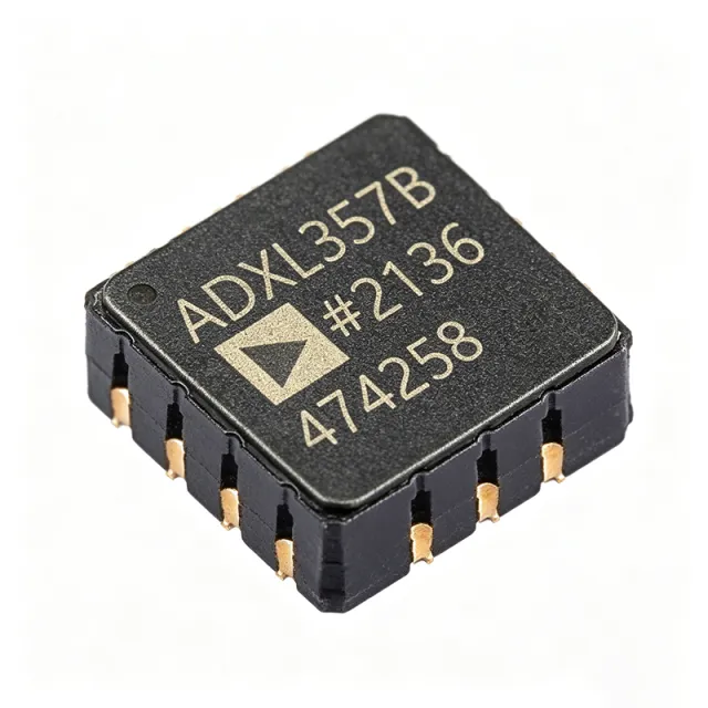
ADXL357BEZ - Low Noise 3-Axis MEMS Accelerometer | Analog Devices
The ADXL357BEZ is a low noise density, low 0 g offset drift, low power, 3-axis MEMS accelerometer from Analog Devices with selectable measurement ranges of ±10g, ±20g, and ±40g. It features a digital output via SPI or I2C interface and is housed in a 14-terminal CLCC package measuring 6mm x 6mm. The device operates over a bandwidth of 1 Hz to 1 kHz and is designed for high-performance industrial and instrumentation applications. An accelerometer is a sensor that measures proper acceleration, which is the rate of change of velocity of a body in its own instantaneous rest frame. MEMS (Micro-Electro-Mechanical Systems) accelerometers are micro-machined devices that integrate mechanical sensing elements with electronic circuitry on a single chip. They are widely used in motion sensing, vibration monitoring, and inertial navigation systems. The ADXL357BEZ belongs to the category of digital-output accelerometers, which convert the sensed acceleration into a digital signal for direct interfacing with microcontrollers or digital signal processors. Key features of the ADXL357BEZ include ultra-low noise density of 80 µg/√Hz, low 0 g offset drift of less than 0.75 mg over temperature, and low power consumption of 200 µA at 3.3 V. The device supports both SPI and I2C digital interfaces, allowing flexible integration into various system architectures. It also includes an integrated temperature sensor and a 32-level FIFO buffer to reduce host processor loading. The ADXL357BEZ utilizes a capacitive sensing element with a high-resolution sigma-delta ADC, providing excellent linearity and stability. The device is factory-calibrated for sensitivity and offset, minimizing the need for user calibration. Its low noise and low drift characteristics make it suitable for precision applications such as structural health monitoring, platform stabilization, and seismic sensing. Typical applications include industrial vibration monitoring, inertial measurement units (IMUs), robotics, and aerospace navigation systems. The device's wide measurement range and high bandwidth enable it to capture both low-frequency tilt and high-frequency vibration signals. Its low power consumption makes it ideal for battery-powered wireless sensor nodes. When designing with the ADXL357BEZ, ensure proper power supply decoupling with a 0.1 µF capacitor close to the VDD pin and a 1 µF capacitor on the VDD I/O pin. The device requires a supply voltage between 2.25 V and 3.6 V, and the digital interface voltage can be set independently via the VDD I/O pin. Careful PCB layout with a solid ground plane is recommended to minimize noise coupling.
ADXL357BEZ-RL - 3-Axis Digital Accelerometer | Analog Devices
The ADXL357BEZ-RL is a low noise density, low 0 g offset drift, low power, 3-axis accelerometer from Analog Devices with selectable measurement ranges of ±10g, ±20g, and ±40g. It provides digital output via SPI or I2C interface and is housed in a 14-lead CLCC (6mm x 6mm) package. The device operates over a bandwidth of 1Hz to 1kHz and is designed for high-performance industrial and instrumentation applications. An accelerometer is a sensor that measures proper acceleration, which is the rate of change of velocity per unit time. The ADXL357 is a MEMS capacitive accelerometer that converts mechanical displacement into an electrical signal, which is then digitized by an onboard ADC. It belongs to the category of inertial sensors, which are essential for motion detection, vibration monitoring, and tilt sensing. The ADXL357 family includes the analog output ADXL356 and the digital output ADXL357, with the ADXL357B variant supporting additional interface options. Key features of the ADXL357BEZ-RL include ultra-low noise density (typically 80 µg/√Hz), low 0 g offset drift over temperature, and low power consumption (typically 150 µA at 3.3V). The selectable measurement ranges allow the user to optimize resolution and dynamic range for specific applications. The device also includes an integrated temperature sensor and a 32-level FIFO buffer to reduce host processor loading. The ADXL357 uses a MEMS capacitive sensing element with a precision analog front-end and a 20-bit digital output. The device features a programmable high-pass filter and low-pass filter, enabling flexible signal conditioning. The SPI and I2C interfaces allow easy integration with microcontrollers and digital signal processors. The 14-lead CLCC package provides a compact footprint with excellent thermal and mechanical stability. Typical applications include structural health monitoring, condition monitoring of rotating machinery, inertial measurement units (IMUs), platform stabilization, and seismic sensing. The low noise and low drift characteristics make it suitable for precision tilt and vibration measurements. The wide bandwidth supports both static and dynamic acceleration measurements. When designing with the ADXL357BEZ-RL, ensure proper decoupling of the power supply and careful PCB layout to minimize noise coupling. The device requires an external pull-up resistor on the I2C lines if used in I2C mode. The FIFO can be configured to reduce interrupt overhead in high-sample-rate applications.
ADXL357BEZ-RL7 - Low Noise 3-Axis MEMS Accelerometer | Analog Devices
The ADXL357BEZ-RL7 is a low noise density, low 0 g offset drift, low power, 3-axis MEMS accelerometer from Analog Devices. It offers selectable measurement ranges of ±10g, ±20g, and ±40g, with a bandwidth of 1 Hz to 1 kHz. The device is housed in a 14-terminal CLCC package measuring 6 mm x 6 mm, suitable for surface mount assembly. It features a digital SPI interface for communication with microcontrollers and processors. An accelerometer is a sensor that measures proper acceleration, which is the rate of change of velocity of a body in its own instantaneous rest frame. MEMS accelerometers are micro-electromechanical systems that integrate mechanical and electrical components on a single chip. They are widely used in inertial measurement units (IMUs), vibration monitoring, and tilt sensing. The ADXL357 belongs to the family of low-noise, low-drift accelerometers designed for precision applications. Key features include ultra-low noise density of 80 µg/√Hz, low 0 g offset drift of 0.75 mg/°C, and low power consumption of 200 µA at 3.3 V. The device operates from a single 2.25 V to 3.6 V supply and includes an internal temperature sensor. It supports both SPI and I2C interfaces, with the ADXL357B variant offering limited I2C. The ADXL357BEZ-RL7 is the reel packaging variant (RL7) of the ADXL357BEZ, which is tray packaged. The ADXL357 uses a capacitive sensing element with a precision analog-to-digital converter (ADC) and digital signal processing. It provides 20-bit resolution and includes a built-in self-test feature. The device is designed for high-performance applications requiring low noise and low drift, such as structural health monitoring, seismic sensing, and platform stabilization. Typical applications include inertial navigation systems, vibration analysis, earthquake detection, and industrial condition monitoring. The low noise and low drift make it ideal for precision measurement over extended periods. The device is also suitable for tilt sensing in robotics and autonomous vehicles. When designing with the ADXL357, ensure proper decoupling of the power supply and careful PCB layout to minimize noise. The device requires an external capacitor on the VDD pin and a pull-up resistor on the SPI lines. The operating temperature range is -40°C to +125°C, making it suitable for harsh environments.

ADXRS453BEZ - ±300°/s Digital Gyroscope | Analog Devices
The ADXRS453BEZ is a high-performance, digital-output angular rate sensor (gyroscope) from Analog Devices, designed for industrial, instrumentation, and stabilization applications in high-vibration environments. It features an advanced differential quad-sensor design that rejects linear acceleration, enabling accurate rate sensing even under shock and vibration. The device measures angular rates up to ±300°/s with a bandwidth of 77.5 Hz and communicates via a 4-wire SPI interface. It operates from a single 3.3 V to 5 V supply and is available in a 16-lead plastic cavity SOIC (SOIC_CAV) package, which is surface-mount compatible. A gyroscope is a sensor that measures angular velocity (rate of rotation) around one or more axes. The ADXRS453 is a single-axis (yaw) gyroscope, detecting rotation around the vertical axis. It belongs to the family of MEMS (Micro-Electro-Mechanical Systems) gyroscopes, which use vibrating mechanical elements to sense Coriolis forces. In the hierarchy of motion sensors, gyroscopes are a subset of inertial sensors, which also include accelerometers and magnetometers. The ADXRS453's digital output simplifies integration with microcontrollers and DSPs, eliminating the need for external analog-to-digital converters. Key features include ultra-high vibration rejection of 0.01°/s/g, excellent null offset stability of 16°/hr, and a wide operating voltage range. The device also offers an internal temperature sensor and a self-test function, which are critical for safety-critical applications. The SPI interface supports daisy-chaining and multiple device configurations, making it suitable for multi-axis systems. The SOIC_CAV package provides a robust, hermetically sealed enclosure that protects the MEMS element from environmental stress. Technically, the ADXRS453 uses a differential quad-sensor architecture that cancels common-mode linear acceleration, resulting in superior vibration immunity compared to single-mass designs. The digital output is a 16-bit word representing angular rate, with a scale factor of 80 LSB/°/s. The device includes an internal voltage regulator, ensuring stable operation across the supply range. The SPI interface operates at clock frequencies up to 2 MHz, allowing high-speed data acquisition. Typical applications include platform stabilization for cameras and antennas, inertial measurement units (IMUs) for robotics and UAVs, industrial machinery monitoring, and medical instrumentation such as surgical tools. The ADXRS453's high vibration rejection makes it ideal for mounting near engines or motors where vibration is prevalent. When designing with the ADXRS453, ensure proper PCB layout with a solid ground plane and decoupling capacitors close to the supply pins. The SPI lines should be kept short and shielded to minimize noise. The device's self-test feature should be exercised during system startup to verify functionality.

ADXRS453BRGZ - ±300°/s SPI Gyroscope | Analog Devices
The ADXRS453BRGZ is a high-performance, single-axis MEMS angular rate sensor (gyroscope) from Analog Devices, designed for precision yaw-rate sensing in demanding industrial, instrumentation, and stabilization applications. It measures angular rate around the Z-axis (yaw) with a full-scale range of ±300°/s and provides digital output via an SPI interface. The device is housed in a 16-pin SOIC-CAV package, operates over a temperature range of -40°C to +105°C, and requires a supply voltage between 3.15V and 5.25V. A MEMS gyroscope is a micro-electromechanical system that measures angular velocity using the Coriolis effect. Unlike traditional mechanical gyroscopes, MEMS gyroscopes are compact, low-power, and highly reliable, making them ideal for integration into electronic systems. The ADXRS453 belongs to the family of angular rate sensors, which are essential components in inertial measurement units (IMUs), motion control systems, and stabilization platforms. Its advanced differential quad sensor design rejects linear acceleration, ensuring accurate rate sensing even in high-vibration environments. Key features of the ADXRS453BRGZ include a digital SPI output with 16-bit resolution, a bandwidth of 77.5Hz, and a -3dB bandwidth of 775Hz. The device offers excellent bias stability and low noise, making it suitable for precision applications. It also includes an internal temperature sensor and self-test capability, enhancing system reliability. The SOIC-16 package is compact and surface-mountable, facilitating PCB integration. Technically, the ADXRS453 uses a vibrating MEMS structure that responds to angular rate through Coriolis acceleration. The differential quad sensor design cancels common-mode linear accelerations, providing robust performance in harsh environments. The SPI interface allows direct digital readout of angular rate, simplifying system design and eliminating the need for external ADC. The device's low power consumption (6mA typical) and wide supply range make it versatile for battery-powered and industrial systems. Typical applications include platform stabilization, inertial navigation, robotics, and industrial automation. In platform stabilization, the ADXRS453 provides real-time rate feedback to control motors and gimbals, ensuring precise orientation. In inertial navigation, it is used alongside accelerometers to track position and orientation. Its high vibration immunity makes it ideal for industrial machinery monitoring and automotive stability systems. When designing with the ADXRS453BRGZ, ensure proper decoupling of the power supply and careful PCB layout to minimize noise. The SPI interface should be isolated from high-current traces to prevent interference. Additionally, consider the device's bandwidth and noise characteristics when designing the control loop to achieve optimal performance.

AIS2IH - 3-Axis Accelerometer, 2g/4g/8g/16g | STMicroelectronics
The STMicroelectronics AIS2IH is a high-performance, low-power 3-axis linear accelerometer designed for automotive and industrial applications. It features a full-scale range of ±2g, ±4g, ±8g, and ±16g, selectable via the I2C/SPI interface, and is packaged in a compact 12-pin LGA (2x2 mm) package. The device operates from a 1.71V to 3.6V supply voltage and includes an integrated temperature sensor, making it suitable for a wide range of motion-sensing and vibration-monitoring applications. An accelerometer is a sensor that measures proper acceleration (the rate of change of velocity) along one or more axes. The AIS2IH is a MEMS (Micro-Electro-Mechanical Systems) capacitive accelerometer, which detects changes in capacitance caused by the displacement of a proof mass under acceleration. It belongs to the broader category of inertial sensors, which also includes gyroscopes and magnetometers. In a typical system hierarchy, the accelerometer is a key component of an inertial measurement unit (IMU), which is used in applications such as vehicle stability control, industrial vibration monitoring, and tilt sensing. Key features of the AIS2IH include a selectable full-scale range of ±2g/±4g/±8g/±16g, a low noise density of 90 µg/√Hz, and a wide operating temperature range of -40°C to +105°C. The device supports both I2C and SPI digital interfaces, with a maximum SPI clock frequency of 10 MHz and I2C clock frequency of 400 kHz. It also features a 32-level FIFO buffer, an embedded temperature sensor, and a programmable interrupt generator for motion detection, free-fall detection, and 6D orientation detection. The AIS2IH is built using ST's advanced MEMS process, which ensures high reliability and long-term stability. The device includes a self-test capability that allows the user to verify the functionality of the sensing element and the signal chain. The low power consumption, typically 180 µA in normal mode and 1.6 µA in power-down mode, makes it ideal for battery-powered applications. The device also supports a wide range of output data rates from 1 Hz to 1000 Hz, allowing the user to trade off power consumption against measurement resolution. Typical applications include automotive airbag systems, electronic stability control, industrial vibration monitoring, and tilt sensing for leveling equipment. The AIS2IH is also suitable for IoT devices that require motion detection and activity monitoring. Its small footprint and low power consumption make it easy to integrate into space-constrained designs. When designing with the AIS2IH, it is important to ensure proper PCB layout to minimize mechanical stress on the sensor. The device should be placed away from high-frequency switching components and vibration sources. Additionally, the I2C/SPI interface lines should be kept short and properly terminated to avoid signal integrity issues.
AS7030B - PPG/ECG Biosensor Module I2C | ams OSRAM | Wearables
The ams OSRAM AS7030B is a vital-sign biosensor module that combines a photoplethysmography (PPG) optical measurement engine with an embedded electrocardiography (ECG) analog front end, outputting processed data over an I2C interface in a compact surface-mount module package (suffix COLM/COQM). A biometric sensor module is a device that converts physiological signals, such as blood-volume pulse and cardiac bioelectric potentials, into digital data for health-monitoring systems. Within the sensor hierarchy, the AS7030B sits under optical and biometric sensors, spanning PPG sensors, ECG analog front ends, GSR measurement, and skin-temperature sensing in a single integrated solution for wearable electronics. Key features include a low-noise analog front end for ECG signal acquisition, a fully integrated optical solution with synchronized LED drive and photodiode readout, a synchronous demodulator for ambient-light rejection, and an infrared emitter with dedicated photodiode enabling a proximity function. The device also supports GSR (galvanic skin resistivity) measurement and external NTC temperature sensor connection, giving designers four biometric modalities from one footprint. Architecturally, the AS7030B integrates LED drivers, a low-noise transimpedance chain, a synchronous demodulator, and digital control logic on one die, reducing external component count and BOM cost. Time-multiplexed optical measurement with demodulation suppresses DC ambient interference, which is essential for wrist-worn PPG accuracy during motion and daylight exposure. Typical applications include fitness bands, smart watches, sports watches, and smart patches, where its low-power design supports multi-day intervals between battery recharges. It is also suited to clinical-grade HRV recording and cuffless vital-sign prototyping via the AS7030B_EVALKIT_USB and AS7030B_EVALKIT_BT evaluation kits. Design considerations: the ams OSRAM recommended supply scheme uses a clean LDO-fed rail (for example a 4.75V LDO as in the official evaluation kit design); noise on VDD directly degrades ECG and PPG signal quality, so careful power filtering is required. This page synthesizes distributor availability data, the official ams OSRAM datasheet, evaluation-kit documentation, and practical design notes not found in the datasheet alone.
AS7030B-COLM - PPG+ECG Biosensor Module I2C | ams OSRAM
The ams OSRAM AS7030B-COLM is a fully integrated vital-sign biosensor module combining photoplethysmography (PPG) optical sensing with an embedded electrocardiogram (ECG) analog front-end (AFE), delivering data over an I2C interface in a 22-pad OLGA22 package (ordering code OLGA22 LF, tape and reel). Its three headline characteristics are dual-modality PPG + ECG heart-rate monitoring, a compact OLGA22 land-grid form factor for space-constrained wearables, and a low-power architecture targeted at -30C to +70C operation. A biosensor module of this type integrates optical emitters (LEDs), photodetectors, an analog front-end, and a programmable sequencer into a single optical subassembly, offloading the host microcontroller from timing-critical LED/PD control. In the wearable system hierarchy, it sits above discrete LED-plus-photodiode pairs and below complete health watch platforms, acting as the sensor-layer heart-rate and biopotential acquisition engine. Key features include the embedded ECG AFE that, per ams documentation, meets IEC 60601-2-47 requirements for ambulatory ECG equipment, an interrupt output pin (INT) for host notification, and an I2C slave interface at 7-bit address 0x30 (0x60/0x61 in 8-bit write/read format). The integrated sequencer automates LED sampling cycles for PPG pulse-rate measurement. The PPG channel operates by sampling light modulated by blood vessels, which expand and contract with the cardiac pulse, while the ECG channel acquires bioelectric potentials generated by the heart, the reference-standard method for cardiac electrical activity. Combined PPG+ECG data enables pulse transit time and advanced vital-sign computation. Typical applications are fitness bands, smart watches, sports watches, chest/patch ECG+PPG monitors, and smart health patches, where board space and multi-day battery life dominate the design. Design consideration: the OLGA22 package requires careful optical and mechanical integration with skin-contact windows and light-blocking gaskets to achieve clinical-grade signal quality; host firmware must service the INT pin promptly to avoid FIFO overflow. This page synthesizes distributor availability data, drop-in alternative guidance, and practical design notes not found in the manufacturer datasheet alone.
AS7030B-COLT - Biosensor with ECG PPG GSR | ams OSRAM
The ams OSRAM AS7030B-COLT is a multi-parameter biosensor solution with an embedded ECG channel, integrated PPG (photoplethysmography) optical front end, and GSR/bioimpedance measurement capability, housed in a 22-pin OLGA (COLT) package with I2C digital output. A biosensor of this class is a specialized analog front-end (AFE) IC that converts physiological signals - blood-volume pulse via light modulation, bioelectric heart potentials via electrodes, and skin conductance via impedance - into digitized data streams for a host processor. Within the system hierarchy, the AS7030B sits between raw optical and electrode elements and the wearable device's microcontroller, functioning as the signal-conditioning and digitization layer of the health-monitoring subsystem. Key features include the embedded ECG channel with electrode inputs for direct bioelectric signal capture, an I2C slave interface using 7-bit address 0x30 (60h write / 61h read in 8-bit format), an interrupt output pin (INT) for host notification, and an enable pin (EN) for switching between normal operation and shutdown mode. According to ams OSRAM documentation, the device does not require a specific power-up sequence and requires a supply voltage of approximately 3.8V for correct operation. Technical depth: the AS7030B operates on the photoplethysmography (PPG) principle - sampling light modulated by blood vessels that expand and contract with each heartbeat - combined with electrocardiography (ECG), the reference standard for measuring bioelectric potentials generated by the heart. The integrated architecture reduces external component count and bill-of-material cost for multi-modal vital-sign designs. Typical applications include fitness bands, smart watches, sports watches, and smart patches, where the AS7030B's low-power design and small form factor suit limited board space and multi-day battery-life targets, as well as patient-monitoring patches and diagnostic wearables. Design consideration: for evaluation and prototyping, ams OSRAM supplies the AS7030B Eval Kit, which isolates the electrodes from mains-referenced USB power via an IEC 60601-1 compliant RECOM DC-DC converter (R0.25S-0505/H or R0.25S-0505/HP) and signal isolator ICs - a safety pattern worth replicating in end designs. This page synthesizes distributor availability, package data, drop-in variant information, and practical design notes not consolidated in the manufacturer datasheet, with pricing and stock status as of 2026-10-11.
AS7050 - PPG/ECG Biosignal AFE, 8 LED Drivers | ams OSRAM
The ams OSRAM AS7050 is a biosignal sensor analog front-end (AFE) that provides up to 8 LED driver outputs, samples up to 6 photodiode inputs, and supports external electrodes, all housed in a small Wafer-Level Chip-Scale Package (WLCSP) with I2C output. It enables synchronized PPG and ECG acquisition in a single vital-sign sensing IC. A biosignal analog front-end is the mixed-signal circuit stage that converts weak physiological signals - optical photoplethysmogram (PPG) current from photodiodes, electrical electrocardiogram (ECG) potentials from skin electrodes, and galvanic skin resistance (GSR) - into digitized data for a host microcontroller. Within the signal-chain hierarchy, the AFE sits between the raw sensor elements (LEDs, photodiodes, electrodes) and the digital processing domain, making it the precision heart of any wearable health monitoring system. Key differentiating features include up to 8 LED driver outputs and 6 photodiode input pins, giving exceptional flexibility for multi-wavelength, multi-site optical arrangements in reflective or transmissive PPG topologies. The embedded low-noise ECG analog front-end meets IEC 60601-2-47 requirements, a significant advantage for medical-grade designs. Synchronized PPG and ECG acquisition enables advanced parameters such as pulse transit time and blood-pressure trend estimation. The thin WLCSP profile suits height-constrained products such as true wireless earbuds, smart rings, and watch backplates. Architecturally, the AS7050 is the next generation of the ams OSRAM vital-sign sensor family, integrating low-noise transimpedance paths, programmable LED current sources, an electrode-based ECG channel, and a GSR measurement stage under I2C control. Flexible time-slot scheduling allows PPG, ECG, and GSR acquisitions to be interleaved with low average power, critical for battery-operated wearables. Typical applications include optical heart-rate and ECG monitoring platforms, smartwatch and fitness-band sensor stacks, hearable in-ear PPG for earbuds, and connected medical and health devices requiring multi-modal biosignal capture. The multi-LED/multi-PD arrangement supports SpO2-style dual-wavelength configurations without external analog circuitry. Design consideration: the WLCSP package requires accurate pad-matched PCB land patterns and careful LED optical crosstalk management; keep photodiode input traces short and shielded to preserve the low-noise front-end performance. This page synthesizes distributor sourcing data, drop-in variant options, and practical design guidance not found in the manufacturer short datasheet, with all key values verified against ams OSRAM and Mouser sources as of 2026-10-11.
AS7050-BWLM - Biosignal AFE PPG/ECG/GSR, I2C | ams OSRAM
The ams OSRAM AS7050-BWLM is a biosignal sensor analog front end (AFE) for vital sign monitoring, supporting photoplethysmogram (PPG), electrocardiogram (ECG), and galvanic skin resistance (GSR) measurement with an I2C digital output interface, housed in a wafer-level package (WLP, lead-free, tape and reel). An analog front end is the signal-chain block that sits between raw physiological sensors and a digital processor. In wearables and medical monitoring devices, the AFE conditions, amplifies, filters, and digitizes tiny biosignals - microvolt-level ECG potentials or nanoamp-scale photodiode currents from PPG - before they reach the microcontroller. The AFE therefore sits within the biosensor hierarchy between the optical/electrode sensor elements and the system's digital signal processing stage. Key differentiating features of the AS7050 include multi-modal biosignal support: PPG is the most used heart-rate monitoring (HRM) method, measuring pulse rate by sampling light modulated by blood vessels that expand and contract as blood pulses through them; ECG captures the heart's electrical activity; and GSR tracks skin conductance for stress and hydration metrics. Integration of these three modalities in one device lets designers build multi-parameter health wearables with a single AFE. The I2C output simplifies host integration, and the WLP package supports the miniature form factors demanded by smartwatches, fitness bands, and earbuds. Per the ams AG datasheet (19 pages, File Size 1,016 Kbytes), the AS7050-BWLM is described as the next-generation vital sign sensor platform. Its architecture combines low-noise analog readout channels for optical and electrode inputs with flexible LED drive capability for PPG, allowing optimized signal-to-noise ratio at low power - critical for battery-operated continuous monitoring. Typical applications include wrist-worn heart-rate and SpO2 monitors, chest-strap and patch ECG recorders, stress-tracking wearables using GSR, and clinical-grade remote patient monitoring peripherals. Any design needing PPG, ECG, and GSR from a single small-footprint front end is a natural fit. A key design consideration: biosignal quality depends heavily on PCB layout discipline - keep the high-impedance ECG electrode inputs short and guarded, and isolate optical channels from digital switching noise; consult the ams OSRAM reference designs for wearable optical placements. This page synthesizes distributor availability from DigiKey, Mouser, and Octopart, datasheet sourcing links, and drop-in alternative analysis not consolidated in the manufacturer datasheet alone.

ASM330LHH - 6-Axis Inertial Measurement Unit | STMicroelectronics
The ASM330LHH is a high-performance 6-axis inertial measurement unit (IMU) from STMicroelectronics, combining a 3-axis accelerometer and a 3-axis gyroscope in a single compact LGA-14 package. It is designed for automotive and industrial applications requiring precise motion sensing, featuring a full-scale range of ±2/±4/±8/±16 g for acceleration and ±125/±250/±500/±1000/±2000 dps for angular rate. The device operates from a 1.71V to 3.6V supply voltage and communicates via I2C or SPI interfaces, with a programmable data rate up to 6.66 kHz for the accelerometer and gyroscope. An inertial measurement unit (IMU) is a sensor that measures linear acceleration and angular velocity using accelerometers and gyroscopes. IMUs are essential in motion tracking, navigation, and stabilization systems, providing the raw data needed for orientation estimation and dead reckoning. The ASM330LHH integrates both sensing elements with a dedicated signal processing chain, enabling high-accuracy measurements in a small footprint. As a 6-axis IMU, it belongs to the broader category of motion sensors, which are critical components in automotive safety systems, industrial robotics, and IoT devices. Key features of the ASM330LHH include a low noise density of 90 µg/√Hz for the accelerometer and 4 mdps/√Hz for the gyroscope, ensuring high-resolution measurements. It also offers an embedded temperature sensor, a 2 KB FIFO buffer for data batching, and advanced power management with a low-power mode consuming only 0.9 mA. The device is AEC-Q100 qualified, making it suitable for automotive applications, and supports a wide operating temperature range of -40°C to +105°C. The LGA-14 package measures 2.5 mm x 3.0 mm, enabling compact PCB designs. Technically, the ASM330LHH uses a MEMS (Micro-Electro-Mechanical Systems) capacitive sensing element for both acceleration and angular rate, with a 16-bit digital output. The device includes an internal voltage regulator, eliminating the need for external regulation, and features a self-test capability for functional safety. The SPI interface supports data rates up to 10 MHz, while I2C operates up to 400 kHz. The FIFO buffer can be configured to store up to 2 KB of data, reducing host processor load. The device also supports interrupt generation for data-ready, FIFO threshold, and motion detection events. Typical applications include automotive electronic stability control (ESC), inertial navigation systems, industrial robotics, and platform stabilization. The ASM330LHH's high shock tolerance of 10000 g and robust design make it ideal for harsh environments. In automotive ESC, the IMU provides real-time yaw rate and lateral acceleration data, enabling precise vehicle dynamics control. In industrial robotics, it enables accurate motion feedback for precise positioning and vibration monitoring. When designing with the ASM330LHH, ensure proper decoupling with a 100 nF capacitor on the power supply pins and place the device close to the mechanical center of rotation for accurate angular rate measurements. The SPI interface should be used for high-speed data streaming, while I2C is suitable for lower data rates. The device's power-down mode reduces current consumption to 1 µA, making it suitable for battery-powered applications.
ASM58012 - 30-Bit Multiturn Absolute Encoder | Pepperl+Fuchs
The Pepperl+Fuchs ASM58012 (ASM58-0 series) is a 30-bit multiturn absolute rotary encoder in an industrial standard ∅58 mm housing with recessed hollow shaft, delivering a 30-bit multiturn position value over an optically isolated RS-422 interface at data transfer rates up to 2 MBaud, with an integrated zero-set function. An absolute rotary encoder is a position sensor that outputs a unique digital code for every shaft angle, unlike incremental encoders which only emit pulses relative to a reference point. In a multiturn absolute encoder, the singleturn position is supplemented by a geared internal multi-turn counter, so the exact shaft position is retained even across power cycles and full shaft rotations. Within the measurement hierarchy, it belongs to the family: position sensor -> rotary encoder -> absolute rotary encoder -> multiturn absolute rotary encoder. Key features include the 30-bit multiturn resolution, which resolves both fine angle and complete revolutions without external counters; the optically isolated RS-422 (SSI-compatible) interface, which protects the controller from ground potential differences in noisy industrial environments; transfer rates up to 2 MBaud for fast cyclic position polling; and a recessed hollow shaft that simplifies mechanical coupling to motor or machine shafts. The ASM58-0 series uses optical scanning technology in a rugged industrial-grade housing, making it suitable for continuous duty on machines that demand repeatable absolute positioning. The zero-set function allows the operator to redefine the reference position electrically, eliminating time-consuming mechanical re-alignment during commissioning or after tooling changes. Typical applications include servo drive and motion-control positioning, factory automation and robotics, cranes and hoisting equipment, and heavy machinery such as packaging lines and material handling systems, where loss of position after power-down would otherwise force a slow homing cycle. When integrating the encoder, verify supply voltage, shaft diameter, and output code configuration against the exact ASM58-0 ordering code, since the family covers multiple electrical and mechanical variants under the same base designation. This page synthesizes verified manufacturer data, family variant cross-references, and practical integration guidance not found on the manufacturer datasheet alone.
AWRL6844 - 57-64GHz Automotive mmWave Radar Sensor | Texas Instruments
The Texas Instruments AWRL6844 is a single-chip, high-performance, low-power 57GHz to 64GHz FMCW mmWave radar sensor designed for automotive in-cabin applications such as child presence detection, intrusion monitoring, and occupancy detection. It operates in the 57GHz to 63.9GHz band with up to 7GHz continuous chirp bandwidth and integrates a radar front-end, processing cores, and a Hardware Security Module (HSM). A mmWave radar sensor is a radar device that transmits and receives millimeter-wave electromagnetic signals (here 57 to 64GHz) and processes frequency-modulated continuous wave (FMCW) reflections to measure range, velocity, and angle of objects. Within the sensing hierarchy, it belongs to: radar sensor -> mmWave sensor -> integrated RF SoC -> semiconductor sensor device. The AWRL6844 belongs to the AWRL684x automotive family, alongside the related AWRL6843. Key features include the 57-64GHz band with 7GHz continuous chirp bandwidth for fine range resolution, an integrated Hardware Security Module (HSM) for secure in-cabin sensing, TI's low-power 45nm RF CMOS process enabling unprecedented integration in an extremely small form factor, and a compact 10.4 x 10.4 mm package suitable for hidden in-cabin mounting. The device is built for self-monitored, ultra-accurate radar systems in the automotive space. Technically, the AWRL6844 integrates a fully programmable radar front-end with an ARM Cortex-R4F processing core and hardware FFT acceleration on a single die, reducing BOM cost and board area versus discrete RF-plus-MCU solutions. Communication interfaces include CAN, I2C, LIN, SPI, and UART outputs (as seen on the AWRL6844DBGANCRQ1 device variant), enabling direct integration into vehicle body and domain controller networks. Typical applications include child presence detection (CPD) for Euro NCAP requirements, intrusion monitoring for anti-theft, occupancy detection for seatbelt and airbag logic, and gesture or vital-sign sensing inside the vehicle cabin. The 60GHz-class band and 7GHz bandwidth allow detection of micro-movements such as breathing even through seat covers. Design consideration: the AWRL6844 uses a different SDK and register/memory map than the earlier IWR6843, so migration requires software rework even where hardware function is similar. Plan for the MMWAVE L-SDK and Code Composer Studio device support packages early in development. Pricing and packaging details should be verified with TI or distributors as of 2026-08-29.
BA76220 - PIR Sensor Controller, 12µA Low Power, 1-Wire | Holtek
The Holtek BA76220 is a dedicated controller IC for human infrared (PIR) sensing applications, integrating a low-noise analog front-end (AFE) and a low-power digital control core in a single chip. According to the Holtek product page, it draws only 12µA quiescent current and supports 1-wire slave communication, which simplifies PCB routing and reduces wiring cost in multi-node sensor networks. The part provides multi-functional output control and is intended for high-sensitivity motion-detection end equipment such as automatic lighting, security alarms, and energy-saving occupancy switches. A PIR controller is a mixed-signal integrated circuit that interfaces directly with a pyroelectric infrared sensor and converts the small analog motion-induced voltage pulses into a digital trigger for downstream actuators. Within the broader system hierarchy, the BA76220 sits below the application layer (lighting, alarms) and above the sensor transducer, providing the analog conditioning, motion validation logic, and timing functions that a discrete op-amp + MCU solution would otherwise require. Holtek's product taxonomy places this part under PIR Controllers within their Touch/Proximity & Peripheral MCU family. Key features include the integrated 12µA AFE, 1-wire slave communication mode, an adjustable delay time platform covering 0.5s to 6h, and multi-functional output control. The integrated AFE eliminates external op-amp and filter components that designers would normally need to condition the PIR signal, while the 1-wire interface allows multiple BA76220 nodes to share a single data line back to a host MCU for centralized control. The adjustable delay platform covers common application timing from a few hundred milliseconds up to half a day, allowing a single SKU to serve both fast security loops and slow occupancy controls. Technically, the BA76220 combines a low-offset internal amplifier with on-chip threshold comparison and a programmable retriggerable monostable. The 12µA quiescent current is achieved through Holtek's low-power CMOS process and dynamic biasing of the AFE during active sensing windows. Designers configure delay time and sensitivity via simple external resistor selection, which keeps the BOM small and avoids any firmware development cycle. Typical applications include automatic LED lighting controlled by body motion, security alarm systems requiring high-sensitivity intrusion detection, smart home occupancy switches, and industrial energy-saving controls. The wide delay range (0.5s to 6h) makes it suitable for both short-cycle corridor lighting and long-cycle room occupancy applications. When designing with this part, use a proper Fresnel lens to focus IR onto the PIR sensor and place the sensor away from direct airflow sources. Avoid mounting the device near heat-generating components, as thermal gradients can cause false triggering even with proper compensation. This page synthesizes verified distributor data, drop-in alternative recommendations, and practical PCB design notes not found in the manufacturer datasheet alone, helping engineers select and implement the BA76220 with confidence.

ICM-20689 - 6-Axis IMU, DMP, ±32g Accel | TDK InvenSense
The TDK InvenSense ICM-20689 is a high-performance 6-axis MotionTracking device that combines a 3-axis gyroscope, a 3-axis accelerometer, and an embedded Digital Motion Processor (DMP) in a compact 4 mm x 4 mm x 0.9 mm 24-pin QFN package. According to the TDK datasheet, it supports a wide VDD range of 1.71 V to 3.45 V, accelerometer full-scale ranges up to ±32 g, and gyroscope full-scale ranges up to ±2000 dps, with I²C, SPI, and auxiliary I²C interfaces. An Inertial Measurement Unit (IMU) is a sensor module that measures specific force, angular rate, and - in 6-axis variants - orientation via a 3-axis gyroscope and 3-axis accelerometer. IMUs belong to the broader category of MEMS motion sensors and are core elements in inertial navigation, gesture recognition, and stabilization. They sit at the bottom of a hierarchy that runs: IMU -> motion sensor -> MEMS sensor -> semiconductor. The ICM-20689 integrates an on-chip DMP that offloads motion-processing algorithms from the host MCU, reducing system power and enabling sensor fusion at the edge. Key features include a 4-Kbyte FIFO that reduces host-processor wakeups, low-noise gyro bias stability, factory-calibrated scale factors, and an AP_AD5 auxiliary master I²C interface for connecting external sensors such as magnetometers. Programmable interrupts, self-test routines, and wake-on-motion thresholds simplify host integration. An on-chip temperature sensor with digital output is also provided for compensation. Typical applications span consumer drones, VR/AR headsets, robotics, wearable sports devices, IoT edge sensors, and gaming controllers, where the DMP handles gesture fusion and pedometer functions without burdening the application processor. Industrial variants leverage the same hardware platform for asset tracking, platform stabilization, and dead-reckoning assistance.
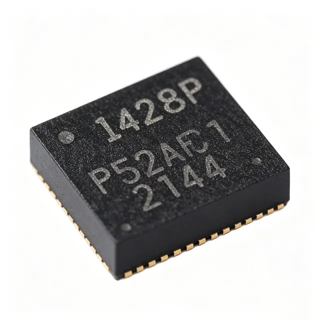
ICM-42688-P - 6-Axis MEMS IMU with 2KB FIFO | TDK InvenSense
The TDK InvenSense ICM-42688-P is a high-precision 6-axis MEMS MotionTracking device that integrates a 3-axis gyroscope and a 3-axis accelerometer in a compact 2.5 x 3.0 x 0.91 mm 14-pin LGA package. It supports I3C, I2C, and SPI serial interfaces, features a 2 kB FIFO, and offers ultralow-power wake-on-motion support to minimize system power consumption. The device is designed for a wide range of motion sensing applications, including drones, robotics, AR/VR, and industrial monitoring. An IMU (Inertial Measurement Unit) is a sensor that measures angular rate and linear acceleration using gyroscopes and accelerometers. The ICM-42688-P combines these into a single package, providing high accuracy and low noise for motion tracking. IMUs are essential in applications requiring orientation and movement detection, such as flight controllers, wearable devices, and navigation systems. The ICM-42688-P is part of the broader category of motion sensors, which includes accelerometers, gyroscopes, and magnetometers, and is a key component in the sensor fusion hierarchy. Key features include a gyroscope noise density of 2.8 mdps/√Hz, an accelerometer noise density of 70 µg/√Hz, and a programmable output data rate up to 32 kHz for the gyroscope and 32 kHz for the accelerometer. The device offers a 2 kB FIFO to reduce bus traffic and system power consumption, and supports a wide supply voltage range of 1.71 V to 3.6 V. It also includes programmable interrupts and a digital motion processor (DMP) for advanced motion processing. The ICM-42688-P utilizes advanced MEMS technology with a low-power architecture, achieving a typical current consumption of 0.9 mA in low-noise mode and 0.45 mA in low-power mode. The device features a temperature range of -40°C to +85°C and is RoHS compliant. Its small footprint and low power make it ideal for battery-powered and space-constrained designs. Typical applications include drone flight controllers, where the ICM-42688-P provides the low noise and high output rate required for stable flight; robotics, for precise motion control and orientation sensing; and AR/VR headsets, for accurate head tracking. The device is also used in industrial monitoring and wearable health devices. When designing with the ICM-42688-P, ensure proper PCB layout with adequate decoupling capacitors on the power supply pins and careful routing of the I2C/SPI lines to minimize noise. The device supports both I2C and SPI, allowing flexibility in system integration.

IIS3DWBTR - Ultra-Wide Bandwidth 3-Axis Digital Vibration Sensor | STMicroelectronics
The STMicroelectronics IIS3DWBTR is an ultra-wide bandwidth, low-noise, 3-axis digital vibration sensor housed in a surface-mount LGA package with solder pads. It integrates a 3-Axis MEMS accelerometer with an on-chip digital interface supporting I2C and SPI, designed for high-fidelity vibration monitoring in industrial environments up to +105 C. According to the manufacturer datasheet, the device delivers a flat frequency response from DC to 6 kHz across all three axes (X, Y, Z), enabling accurate capture of mechanical vibrations in machinery and structural assets. Key specifications include selectable full-scale acceleration ranges of +/-2 g, +/-4 g, +/-8 g, and +/-16 g, along with ultra-low noise density of 75 ug/giB (in the high-performance mode). The on-chip ADC samples at up to 26.7 kHz with a 16-bit resolution, and the FIFO buffer holds up to 3 kB of programmable watermark data. The sensor operates from a 1.71 V to 3.6 V supply and includes a temperature sensor for thermal compensation. The IIS3DWBTR is a system-in-package (SiP) that combines the MEMS element and the ASIC in a single reflow-solderable land-grid-array module. The wide bandwidth, low noise, stable sensitivity, and the ability to operate over an extended temperature range make it particularly suitable for vibration monitoring of motors, pumps, fans, bearings, and structural components in Industry 4.0 deployments. Typical applications include condition monitoring and predictive maintenance in rotating machinery, vibration analysis in HVAC and building automation, motor control feedback loops, structural health monitoring of bridges and towers, and industrial IoT sensor nodes. The wide bandwidth also supports shock detection and seismic instrumentation. When designing with the IIS3DWBTR, place 100 nF decoupling capacitors as close as possible to the supply pins and follow the PCB layout guidelines in the manufacturer datasheet to minimize mechanical stress coupling and ensure accurate high-frequency vibration measurements. The 1.71 V minimum supply makes it directly usable with 1.8 V MCUs and Bluetooth Low Energy SoCs without level shifters. This page synthesizes distributor pricing, drop-in same-package alternatives, and practical design notes not found in the standalone manufacturer datasheet, helping engineers shorten selection cycles for vibration-sensing projects.
LIS2DE12TR - 3-Axis MEMS Accelerometer, 2g/4g/8g/16g | STMicroelectronics
The STMicroelectronics LIS2DE12TR is a low-power, 3-axis linear accelerometer with a digital I2C/SPI serial interface, designed for a wide range of motion-sensing applications. It features user-selectable full-scale ranges of ±2g, ±4g, ±8g, and ±16g, and supports output data rates from 1 Hz to 5.3 kHz. The device operates from a 1.71V to 3.6V supply and is available in a compact 12-lead LGA package (2x2x1 mm), making it ideal for space-constrained portable and wearable designs. An accelerometer is a sensor that measures proper acceleration (the rate of change of velocity) of a body in its own instantaneous rest frame. In the context of MEMS (Micro-Electro-Mechanical Systems), accelerometers typically use capacitive sensing elements to detect changes in capacitance caused by the displacement of a proof mass under acceleration. The LIS2DE12TR belongs to the category of motion sensors, which are a subset of sensors used in electronic systems to detect movement, orientation, and vibration. Motion sensors play a critical role in applications ranging from consumer electronics (smartphones, wearables) to industrial monitoring and automotive safety systems. Key features of the LIS2DE12TR include an ultra-low-power consumption of 2 µA in low-power mode at 10 Hz ODR, a 16-bit data output, and an embedded first-in, first-out (FIFO) buffer that reduces host processor load. The device also integrates a programmable interrupt generator for motion detection, free-fall detection, and 6D/4D orientation detection, enabling always-on functionality with minimal power draw. The I2C and SPI interfaces provide flexibility for system integration, and the device is RoHS compliant and halogen-free. From a technical perspective, the LIS2DE12TR uses a capacitive sensing element with a dedicated ASIC (Application-Specific Integrated Circuit) for signal conditioning and digital conversion. The device includes a self-test capability that allows verification of the sensing element and electronics, and it operates over a temperature range of -40°C to +85°C. The LGA package is designed for surface-mount assembly and is compatible with standard reflow soldering processes, with a moisture sensitivity level (MSL) of 1. Typical applications include motion-activated user interfaces, orientation detection in portable devices, vibration monitoring in industrial equipment, and activity tracking in wearables. The low power consumption and small footprint make it particularly suitable for battery-powered IoT devices and smart home sensors. When designing with the LIS2DE12TR, ensure proper decoupling of the power supply with a 100 nF capacitor placed close to the VDD pin, and route the I2C/SPI lines with appropriate pull-up resistors. The interrupt pins can be configured to wake the host processor only when motion is detected, significantly extending battery life in always-on applications.