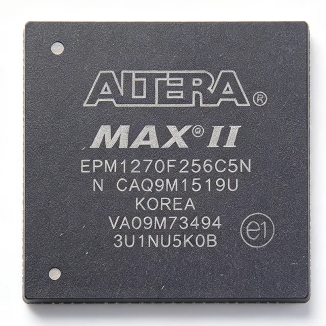
EPM1270F256 - MAX II 980-Macrocell CPLD, 256-BGA | Altera
Артикул: EPM1270F256 ✓ Активен| Кол-во | Цена за ед. | Итого |
|---|---|---|
| 1 | $18.4 | $18,40 |
| 10 | $16.55 | $165,50 |
| 100 | $14.2 | $1.420,00 |
| 500 | $12.1 | $6.050,00 |
| 1.000 | $10.85 | $10.850,00 |
EPM1270F256 Обзор
A CPLD (Complex Programmable Logic Device) is a non-volatile programmable logic device that combines the architectural simplicity, deterministic timing, and instant-on behavior of classic PAL/GAL logic with modern high-pin-count integration. Within the broader programmable-logic taxonomy, the MAX II family sits between simple 5-V SPLDs and high-density SRAM-based FPGAs: like SPLDs it is non-volatile and pin-configurable, but like an FPGA it integrates thousands of gates and dozens of I/O standards. MAX II devices are widely used as interface bridges, I/O expanders, and timing controllers in cost-sensitive industrial and consumer systems.
Key features of the EPM1270F256 include 980 macrocells / 1270 logic elements, 8 Kbits of user flash memory, on-chip voltage regulators supporting 3.3 V, 2.5 V, 1.8 V, and 1.5 V operation, MultiVolt core and I/O supporting mixed-voltage interfacing, JTAG (IEEE 1149.1) boundary-scan programming, and an instant-on configuration time measured in microseconds. The 256-pin FineLine BGA footprint provides flexible I/O bank placement while preserving vertical migration to the EPM570 and EPM2210 in the same package.
Architecturally, the EPM1270F256 implements the Logic Array Block (LAB) structure with 16 macrocells per LAB, a fast t<sub>PD</sub> in the single-digit nanosecond range, and a deterministic interconnect that makes it well-suited for I/O glue, address decoding, register insertion, and state-machine implementation. The non-volatile flash cell removes the need for a separate configuration PROM, lowering BOM cost and enabling secure in-system updates via JTAG.
Typical applications include bus-interface bridging (e.g., PCI to local bus), I/O expansion and voltage translation, power-up sequencing logic, motor-control and industrial automation glue, LED display driving and refresh, and consumer-electronics control logic where instant-on behavior and low unit cost matter more than raw logic density.
When designing with the EPM1270F256, ensure that the chosen I/O standard matches the bank's VCCIO supply and respect the device's MultiVolt I/O rules when bridging 1.5 V, 1.8 V, 2.5 V, and 3.3 V domains. Decoupling must follow the Quartus II power-pin guidance; leaving the on-chip regulator's decoupling incomplete can cause VCCINT ripple that degrades t<sub>PD</sub> margins.
This page synthesizes distributor pricing, drop-in alternatives in the same 256-pin FineLine BGA footprint, and practical design notes drawn from the MAX II handbook to give engineers a single decision-ready view not found in the bare datasheet.
Аналоги без доработки для EPM1270F256 — тот же корпус, pin-to-pin совместимость. Компоненты в других корпусах, требующие переработки PCB, исключены.
Варианты в этой серии
Модели той же серии, совместимые без доработки с EPM1270F256 (тот же форм-фактор и посадочное место) — отличается по Operating Temperature, Package, Programming Interface.
Инструмент быстрого сравнения — выберите альтернативные компоненты для сравнения бок о бок:
EPM1270F256C5
✓ В наличии
$25.4 / шт.
Открыть даташит →EPM1270F256I5N
✓ В наличии
$14.85 / шт.
Открыть даташит →EPM570F256I5N
✓ В наличии
$19.85 / шт.
Открыть даташит →EPM2210F256I5N
📋 Справочный аналог (нет в каталоге)
EPM1270F256C3
📋 Справочный аналог (нет в каталоге)
EPM1270F256C4N
📋 Справочный аналог (нет в каталоге)
EPM1270F256 Максимальные параметры и электрические характеристики
| Family | MAX II |
| Macro Cells (Typical) | 980 |
| Logic Elements | 1270 |
| User I/O (Max) | 212 |
| User Flash Memory | 8 Kbits |
| Supply Voltage (Core) | 2.5 V / 3.3 V (on-chip regulator) |
| I/O Voltages Supported | 1.5 V / 1.8 V / 2.5 V / 3.3 V (MultiVolt) |
| Maximum Frequency | 201.1 MHz |
| Process Technology | 0.18 µm |
| Корпус | 256-Pin FineLine BGA |
| Тип монтажа | Surface Mount |
| Configuration Memory | Non-volatile flash (instant-on) |
| Programming Interface | JTAG (IEEE 1149.1) |
| Рабочая температура | -40C to +100C (industrial, I5N suffix) |
| Статус RoHS | Compliant |
| Vertical Migration | Pin-compatible with EPM570F256 and EPM2210F256 |
Руководство по цоколевке EPM1270F256 в корпусе 256-pin fineline bga
Цоколевка для EPM1270F256 (корпус 256-pin fineline bga). Эта цифровая ИС включает выводы GPIO, интерфейсы связи (UART, SPI, I2C) и выводы питания. Обратитесь к техническому описанию производителя для альтернативных функций выводов и вариантов конфигурации. Необходимо для проектирования встраиваемых систем и трассировки печатных плат.

Нет подробных данных о распиновке для EPM1270F256.
Обратитесь к даташиту для полной конфигурации выводов.
Типичное применение
EPM1270F256 подходит для 7 применениеs: Bus Interface Bridging (PCI / Local Bus), I/O Expansion and Voltage Translation, Power-up Sequencing Controller, Industrial Automation Glue Logic, LED Display Driver and Refresh, Consumer Electronics Control Logic, Motor Control and PWM Generation.
Bus Interface Bridging (PCI / Local Bus)
The EPM1270F256 is widely used as a bus-bridge between legacy parallel buses (PCI, ISA, local bus) and modern processors, where its 212 user I/O and MultiVolt 1.5/1.8/2.5/3.3 V support let one device bridge mixed-voltage domains without external level shifters. The MAX II family's non-volatile instant-on configuration means the bus-bridge logic is active within microseconds of power-up, which is critical for systems that must respond to host enumeration during the BIOS boot phase. The 980-macrocell capacity comfortably absorbs address-decode, wait-state, and interrupt-acknowledge state machines for 32-bit bus widths. Engineers typically place the CPLD adjacent to the bus connector with matched-impedance routing and provide local decoupling on every VCCINT/VCCIO pin per Quartus II power-pin guidance.
Рекомендуется
I/O Expansion and Voltage Translation
The EPM1270F256's MultiVolt I/O banks make it a natural fit for I/O expansion and voltage translation between 1.5 V, 1.8 V, 2.5 V, and 3.3 V peripherals. Up to 212 user I/O can be partitioned into independent banks, each powered from its own VCCIO rail, so a single CPLD can replace dozens of discrete level-shifters and bus-switch ICs while adding glue-logic at the same time. The deterministic pin-to-pin timing of the MAX II architecture is essential for translation paths carrying fast synchronous buses such as SPI, I2C at high speed, or parallel RGB interfaces. Using the CPLD for both translation and control reduces BOM cost, board area, and BOM risk versus a translator-IC-plus-discrete-logic implementation.
Рекомендуется
Power-up Sequencing Controller
Power-up sequencing for multi-rail systems is a textbook MAX II use case, and the EPM1270F256 provides the 212 user I/O and 980 macrocells required to sequence 10+ rails with PG (power-good) feedback. The non-volatile flash configuration ensures the sequencer logic is live within microseconds of VCC applied, well before downstream DC-DC converters reach regulation - this avoids the common glitch where downstream rails come up in the wrong order. PG flags from each regulator feed the CPLD, which then drives the ENABLE pins in the correct order, optionally with adjustable delay generated by internal timers. The 0.18 µm process and modest 2.5/3.3 V core consumption also keep the sequencer's quiescent draw low enough to be powered from an always-on rail.
Рекомендуется
Industrial Automation Glue Logic
In industrial automation, the EPM1270F256 (typically ordered as EPM1270F256I5N for -40C to +100C operation) is used as glue logic between PLC backplanes, motor-control MCUs, and field-bus transceivers. Its 1270 LEs are sufficient to implement custom state machines for encoder quadrature decoding, PWM blanking, and safety-watchdog supervision that off-the-shelf logic ICs cannot deliver. The 256-pin FineLine BGA footprint preserves routing headroom for high-speed differential pairs to RS-485 / CAN transceivers, and the JTAG (IEEE 1149.1) programming interface supports in-system firmware updates without removing the board from the chassis. Industrial users also benefit from the MAX II family's instant-on flash, which avoids the SRAM-FPGA cold-boot delay during emergency-restart events.
Рекомендуется
LED Display Driver and Refresh
The EPM1270F256 is a popular choice for driving large LED sign and dot-matrix displays, where its 212 user I/O pins can multiplex dozens of row/column lines while the 980 macrocells implement PWM dimming, gamma correction, and refresh timing. The MAX II instant-on flash configuration eliminates the cold-boot blank-screen that plagues SRAM-FPGA-based display controllers in outdoor signage applications. Deterministic timing lets the refresh rate be tuned precisely to avoid flicker on-camera, and the on-chip 8 Kbits of user flash can store lookup tables and test patterns that the host MCU writes at boot. MultiVolt I/O means a single CPLD can drive both 3.3 V logic-level shift-registers and 5 V high-current LED drivers in the same design.
Рекомендуется
Consumer Electronics Control Logic
In cost-sensitive consumer products such as set-top boxes, home appliances, and printers, the EPM1270F256 provides the right balance of logic density, I/O count, and unit cost. Designers use it for front-panel button scanning, IR receiver decoding, relay and triac timing, low-speed peripheral multiplexing, and watchdog supervision - tasks that would otherwise require several discrete logic ICs. The MAX II non-volatile configuration means the appliance is functional within microseconds of AC power being applied, an important UX factor in modern consumer devices. MultiVolt I/O bridges between 1.8 V application processors and 3.3 V or 5 V peripheral ICs without external level shifters, keeping the BOM short and the PCB compact.
Рекомендуется
Motor Control and PWM Generation
The EPM1270F256's 1270 LEs and 212 user I/O are well-suited to motor-control glue logic: complementary PWM generation with dead-band insertion, Hall-sensor or quadrature-encoder decoding, fault-input prioritization, and brake/coast sequencing. The MAX II family's deterministic timing guarantees consistent PWM edge placement, which is essential for low-ripple torque output in BLDC and stepper drives. Up to 212 I/O let the CPLD drive gate-driver enable lines, fault-clear lines, and current-sense multiplexers for multi-axis systems without external logic. The non-volatile instant-on configuration is also valuable in safety applications where the motor controller must latch outputs in a known state within microseconds of power-up.
Рекомендуется
Сводка рекомендуемых товаров
Справочные инженерные данные для EPM1270F256 — сравнение, рекомендации по проектированию и информация о соответствии.
Руководство по выбору
Сравнение с аналогами
| Параметр | Этот товар | EPM1270F256C5 | EPM1270F256I5N | EPM570F256I5N | EPM2210F256I5N | EPM1270F256C3 | EPM1270F256C4N |
|---|---|---|---|---|---|---|---|
| Package | 256-Pin FineLine BGA | 256-Pin FineLine BGA (same) | 256-Pin FineLine BGA (same) | 256-Pin FineLine BGA (same) | 256-Pin FineLine BGA (same) | 256-Pin FineLine BGA (same) | 256-Pin FineLine BGA (same) |
| Brand | Altera (Intel PSG) | Altera (Intel PSG) | Altera (Intel PSG) | Altera (Intel PSG) | Altera (Intel PSG) | Altera (Intel PSG) | Altera (Intel PSG) |
| Macro Cells | 980 | 980 | 980 | 440 | 1700 | 980 | 980 |
| Logic Elements | 1270 | 1270 | 1270 | 570 | 2210 | 1270 | 1270 |
| Operating Temperature | 0C to +85C (commercial, base) | 0C to +85C | -40C to +100C (industrial) | -40C to +100C (industrial) | -40C to +100C (industrial) | 0C to +85C | 0C to +85C |
| Speed Grade | Base (unspecified) | -5 | -5 | -5 | -5 | -3 (fastest) | -4 |
| Configuration Memory | Non-volatile flash (instant-on) | Non-volatile flash | Non-volatile flash | Non-volatile flash | Non-volatile flash | Non-volatile flash | Non-volatile flash |
| Programming Interface | JTAG (IEEE 1149.1) | JTAG (IEEE 1149.1) | JTAG (IEEE 1149.1) | JTAG (IEEE 1149.1) | JTAG (IEEE 1149.1) | JTAG (IEEE 1149.1) | JTAG (IEEE 1149.1) |
Ключевые отличия
- Highest density in 256-FineLine BGA at this speed grade (против EPM570F256I5N)
- Vertical-migration family with two density options on the same footprint (против EPM2210F256I5N)
- Non-volatile instant-on flash configuration (против EPM1270F256C3 (same die, faster speed grade))
- Industrial-temperature option in the same package (против EPM1270F256C5 (commercial-temp sibling))
Заметки по проектированию
The EPM1270F256 has on-chip voltage regulators that derive the internal VCCINT from a 2.5 V or 3.3 V VCC supply. Decoupling guidance from the MAX II handbook requires at least one 0.1 µF ceramic capacitor per VCCIO bank plus bulk decoupling on VCC; incomplete decoupling causes VCCINT ripple that degrades t<sub>PD</sub> margins. When operating at the maximum 201.1 MHz f<sub>MAX</sub>, place the bulk capacitor within 25 mm of the VCC pins and use four-layer PCB with dedicated power and ground planes.
The 256-pin FineLine BGA package demands reflow profile per J-STD-020 and PCB pad design per the Altera FineLine BGA land-pattern recommendation (non-solder-mask-defined pads are preferred for FineLine BGA). Signal escape routing should escape on at least two layers between BGA rows using 0.1 mm trace/space to keep the breakout manufacturable on standard 1 oz copper. Matched-impedance routing is required for high-speed I/O such as LVDS, and the entire BGA footprint must be kept away from board edges to avoid warpage cracking.
MultiVolt I/O banks on the EPM1270F256 are powered independently per VCCIO pin, so a single device can bridge 1.5/1.8/2.5/3.3 V domains. Engineers must ensure each bank's VCCIO matches the I/O standard used in that bank; mixing standards across a single bank without reconfiguration is not allowed and will damage the I/O. For high-speed buses (DDR, LVDS), follow the MAX II handbook's termination and length-matching rules, and avoid routing I/O across split power planes that straddle two VCCIO domains.
Common pitfalls include (1) assuming the EPM1270F256 is SRAM-based like a Xilinx Spartan or Altera Cyclone - it is flash-based, so no external boot PROM is needed, and the device is live within microseconds; (2) ignoring the -3/-4/-5 speed-grade suffix and selecting the wrong bin for a tight timing closure; (3) leaving JTAG TCK un-terminated, which can cause boundary-scan failures; and (4) powering a bank from a voltage outside the 1.5-3.3 V MultiVolt range. Always verify the full ordering code (e.g., EPM1270F256I5N) matches the desired temperature and speed grade before placing the order.
Quartus II Floorplan and pin-planner output should drive final PCB pin assignment, but as a rule of thumb place high-speed differential pairs (LVDS, clock outputs) on the package side closest to the on-chip PLL-like clock networks, and group bank-VCCIO pins together. Keep JTAG pins (TDI, TDO, TMS, TCK) accessible for the programming header or flying-lead ISP probe. For vertical-migration designs, reserve identical footprints for EPM570F256 and EPM2210F256 so that a board revision can swap density without PCB rework.
Информация о соответствии
RoHS compliance per Altera/Intel product page; not AEC-Q100 qualified (industrial -40C to +100C only, not full automotive PPAP). Halogen-free status not explicitly stated in the available data and marked unknown per Data Authenticity Rule 2.







