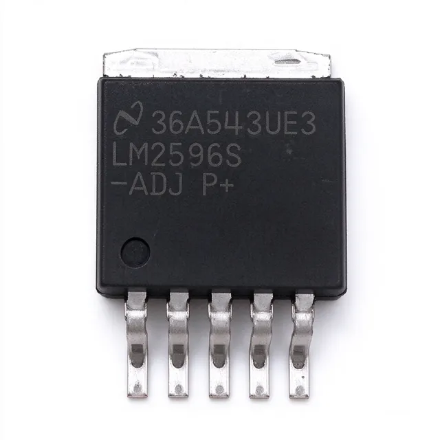
LM2596S-ADJ - 3A Adjustable Step-Down Switcher | Texas Instruments
Артикул: LM2596S-ADJ ✓ Активен| Кол-во | Цена за ед. | Итого |
|---|---|---|
| 1 | $1.4063 | $1,41 |
| 10 | $1.0156 | $10,16 |
| 100 | $0.8984 | $89,84 |
| 500 | $0.8594 | $429,70 |
| 1.000 | $0.8203 | $820,30 |
LM2596S-ADJ Обзор
A buck (step-down) switching regulator is a type of DC-DC converter that uses a power switch, inductor, and rectifier to efficiently lower an input voltage to a lower regulated output. Compared with linear regulators, buck converters dissipate far less power because they switch the pass element fully on or fully off, reaching typical efficiencies of 73% to 88% at 3 A. The LM2596 sits in the classic SIMPLE SWITCHER family: non-isolated, asynchronous, and easy to design around with standard 33 µH inductors and 220 µF output capacitors.
Key features include a fixed 150 kHz internal oscillator, 3 A continuous output current, 4.5 V to 40 V input range, adjustable output from 1.2 V to 37 V (set by external feedback resistors), TTL-shutdown input, internal current limiting, and thermal shutdown. The 5-lead TO-263 (D2PAK) tab provides a low thermal-resistance path that can dissipate the 7 W to 15 W typical full-load losses when soldered to sufficient copper area.
Internally, the LM2596 uses a fixed-frequency, peak-current-controlled control architecture with an external compensation network chosen by the output capacitor type. The datasheet specifies standard and high-efficiency design tables that pair 33 µH inductors with 220 µF output capacitors (standard) or 330 µF with Schottky rectifiers (high-efficiency), giving the designer a proven starting BOM.
Typical applications include 24 V-to-5 V/3.3 V industrial bus conversion, automotive accessory power, hobby robotics and drone LiPo battery regulation, distributed 12 V PoE auxiliary rails, and DIY buck modules. With thousands of third-party modules built around the part, it remains the canonical first buck regulator most engineers cut their teeth on.
When designing, follow the datasheet catch-diode selection carefully: a 3 A Schottky such as the MBR360 keeps efficiency high, while a 1N5822 or similar is acceptable for lower-frequency, lower-cost designs. Keep the input capacitor loop tight and never operate above 40 V input; add a TVS such as P6KE39A for transients beyond 40 V.
This page synthesizes distributor pricing, drop-in alternatives, and practical design notes not found in the manufacturer datasheet alone, giving engineers a single decision-ready view of the LM2596S-ADJ.
Аналоги без доработки для LM2596S-ADJ — тот же корпус, pin-to-pin совместимость. Компоненты в других корпусах, требующие переработки PCB, исключены.
Варианты в этой серии
Модели той же серии, совместимые без доработки с LM2596S-ADJ (тот же форм-фактор и посадочное место) — отличается по Package, RoHS Status, Switching Frequency, Input Voltage Range, Efficiency.
Инструмент быстрого сравнения — выберите альтернативные компоненты для сравнения бок о бок:
LM2596SX-ADJ/NOPB
✓ В наличии
$1.4 / шт.
Открыть даташит →LM2596S-ADJ/NOPB
📋 Справочный аналог (нет в каталоге)
LM2596HV-ADJ
📋 Справочный аналог (нет в каталоге)
XL2596S-ADJ
📋 Справочный аналог (нет в каталоге)
LM2576S-ADJ
📋 Справочный аналог (нет в каталоге)
GS2596-ADJ
📋 Справочный аналог (нет в каталоге)
LM2596S-ADJ Максимальные параметры и электрические характеристики
| Топология | Buck (Step-Down) |
| Тип выхода | Adjustable |
| Диапазон выходного напряжения | 1.2 V to 37 V |
| Максимальный выходной ток | 3 A |
| Диапазон входного напряжения | 4.5 V to 40 V |
| Частота переключения | 150 kHz (fixed, internal oscillator) |
| Напряжение обратной связи | 1.23 V (typical internal reference) |
| Ток покоя | 5 mA (typical, switching) |
| Standby Current (Shutdown) | 50 µA (typical) |
| КПД | 73% to 88% (typical, depends on VIN/VOUT/load) |
| Диапазон рабочих температур | -40 °C to +125 °C |
| Корпус | TO-263-6, D2PAK (5 Leads + Tab), TO-263BA |
| Тип монтажа | Surface Mount |
| Уровень MSL | 3 |
| Статус RoHS | Compliant (lead-free LM2596S-ADJ/NOPB variant) |
Конфигурация выводов LM2596S-ADJ
| Контакт 1 | VIN — Input supply voltage (4.5 V to 40 V) |
| Контакт 2 | OUTPUT — Switch node - connects to inductor and catch diode |
| Контакт 3 | GND — Ground reference |
| Контакт 4 | FEEDBACK — Feedback voltage input (1.23 V reference), set by resistor divider |
| Контакт 5 | ON/OFF — TTL shutdown input (logic-low enables regulator) |
| Контакт 6 | TAB (GND) — Exposed tab - internally tied to GND, solder to PCB copper for heatsinking |
Типичное применение
LM2596S-ADJ подходит для 6 применениеs: 24 V Industrial Bus to 5 V / 3 A Conversion, Automotive 12 V Accessory Power, Hobby Robotics / Drone LiPo Regulation, Distributed 12 V PoE Auxiliary Rails, DIY Buck Modules / Blue LM2596 Buck Boards, Solar Charge Controller Auxiliary Loads.
24 V Industrial Bus to 5 V / 3 A Conversion
The LM2596S-ADJ's 4.5 V to 40 V input range and 3 A output make it the canonical buck converter for 24 V industrial bus systems. Per the TI datasheet design tables, with VIN = 24 V, VOUT = 5 V at 3 A, the regulator hits ~80% efficiency with a 33 µH inductor and MBR360 Schottky; the TO-263 tab dissipates 5-7 W into a 6 cm² copper pour. Engineers value the regulator for PLC I/O, sensor hubs, and motor-driver auxiliary rails because it requires only four external parts, has internal current limit and thermal shutdown, and survives 40 V transients without external TVS.
Рекомендуется
Automotive 12 V Accessory Power
For automotive 12 V battery systems running accessories (LED light bars, fans, USB chargers), the LM2596S-ADJ is well suited because its 40 V input rating covers load-dump transients (with a TVS), and the adjustable output can be set from 1.2 V up to 13 V. Per the TI datasheet, a 12 V-to-5 V / 3 A accessory rail delivers ~85% efficiency with 33 µH/220 µF standard BOM. Add a P6KE39A TVS at the input to clamp load-dump events above 40 V, and place a 470 µF input capacitor to survive cold-crank dips below 6 V.
Рекомендуется
Hobby Robotics / Drone LiPo Regulation
Hobby robotics, drones, and RC vehicles often need 5 V or 12 V rails from a 3 S / 4 S LiPo (12.8 V nominal up to 16.8 V full). The LM2596S-ADJ accepts up to 40 V, so it can ride through the LiPo voltage range while delivering 3 A to servos, BEC circuits, or auxiliary boards. Per the TI datasheet, a 4 S-to-5 V / 3 A supply runs at ~78% efficiency with a 68 µH inductor; pair the TO-263 tab to a small copper pad (~4 cm²) to handle the 8-10 W dissipation during high throttle events.
Рекомендуется
Distributed 12 V PoE Auxiliary Rails
PoE-powered devices need isolated or non-isolated auxiliary rails for fans, LEDs, and control logic. The LM2596S-ADJ handles the post-PoE 12 V bus well, stepping it down to 5 V / 3 A at ~85% efficiency for fan and LED drivers per the TI datasheet design tables. With 33 µH inductor and 220 µF capacitors it forms a stable, low-noise rail; the TO-263 footprint drops onto a 4-layer PoE board alongside the isolated PoE PD controller.
Рекомендуется
DIY Buck Modules / Blue LM2596 Buck Boards
The LM2596S-ADJ is the regulator behind the famous blue 4-pin 'buck converter' modules sold worldwide (In, Out+, Out-, EN). These modules accept 4-40 V, deliver 1.25-35 V at 3 A, and are calibrated with an external multi-turn pot on the feedback divider. Per the TI datasheet BOM, a 33 µH inductor, 470 µF input cap, 220 µF output cap, and MBR360 Schottky form the complete module. The TO-263 tab is soldered to the module's exposed copper pour for heat spreading.
Рекомендуется
Solar Charge Controller Auxiliary Loads
Off-grid solar charge controllers often run from a 24 V battery bus that swings from 20 V to 30 V and must power 5 V / 12 V loads (display, fan, MCU rails). The LM2596S-ADJ is an excellent choice: 40 V input margin covers 30 V battery + transient spikes, 3 A output handles fan + MCU + relay coils, and the TO-263 tab dissipates the 5-10 W losses to PCB copper. Per TI datasheet, a 24 V-to-5 V design runs at ~80% efficiency; a 24 V-to-12 V rail runs at ~92% efficiency.
Рекомендуется
Сводка рекомендуемых товаров
Справочные инженерные данные для LM2596S-ADJ — сравнение, рекомендации по проектированию и информация о соответствии.
Руководство по выбору
Сравнение с аналогами
| Параметр | Этот товар | LM2596S-ADJ/NOPB | LM2596HV-ADJ | XL2596S-ADJ | LM2576S-ADJ | GS2596-ADJ |
|---|---|---|---|---|---|---|
| Package | TO-263-5 (D2PAK) | TO-263-5 (D2PAK) - same | TO-263-5 (D2PAK) - same | TO-263-5 (D2PAK) - same | TO-263-5 (D2PAK) - same | TO-263-5 (D2PAK) - same |
| Brand | Texas Instruments | Texas Instruments | Texas Instruments | XLSemi | Texas Instruments | Globaltech Semiconductor |
| Input Voltage Range | 4.5 V to 40 V | 4.5 V to 40 V | 4.5 V to 60 V | 4.5 V to 40 V | 4.5 V to 40 V | 4.5 V to 40 V |
| Maximum Output Current | 3 A | 3 A | 3 A | 3 A | 3 A | 3 A |
| Switching Frequency | 150 kHz | 150 kHz | 150 kHz | 150 kHz | 52 kHz | 150 kHz |
| Output Voltage Range | 1.2 V to 37 V | 1.2 V to 37 V | 1.2 V to 57 V | 1.2 V to 37 V | 1.2 V to 37 V | 1.2 V to 37 V |
| Efficiency (typical at 3 A) | 73% to 88% | 73% to 88% | 73% to 88% | 70% to 85% | 75% to 88% | 70% to 85% |
| Quiescent Current (switching) | 5 mA | 5 mA | 5 mA | 5 mA | 5 mA | 5 mA |
| RoHS Compliant | Yes (LM2596S-ADJ/NOPB) | Yes | Yes | Varies by part number | Yes (NOPB) | Varies by part number |
Ключевые отличия
- Wide 4.5 V to 40 V input with same TO-263 footprint (против LM2596HV-ADJ)
- 150 kHz switching enables standard 33 µH inductors (против LM2576S-ADJ)
- Cross-brand pin-compatible with XLSemi / Globaltech clones (против XL2596S-ADJ)
Заметки по проектированию
Estimated: at VIN=24V, VOUT=5V, IOUT=3A, regulator dissipates roughly (VIN-VOUT)/VOUT × Pout ≈ 13.6W internally (less in practice given ~80% efficiency, so actual loss ≈ 3.7W). The TO-263 (D2PAK) tab has θJC ≈ 2 °C/W; with at least 6 cm² of 2 oz copper on the PCB tab, θJA drops below 30 °C/W, keeping junction below 125 °C. For VIN above 30 V at full 3 A load, attach an external clip-on heatsink to the tab.
Place the input capacitor, catch diode, and inductor as close to the TO-263 pins as possible to minimize the high-current loop area. Use a 470 µF low-ESR electrolytic (or 220 µF + 1 µF ceramic in parallel) on VIN per the TI LM2596 datasheet design table. The exposed tab must be soldered to a copper pour of at least 6 cm² for reliable 3 A operation; isolated thermal vias are recommended for double-sided boards.
Do not exceed the 40 V absolute maximum input voltage; add a P6KE39A TVS for inductive-load or load-dump transients. The ON/OFF pin is TTL-shutdown and should be tied to GND (logic-low enables regulator) or left open (it has an internal pull-up) - never float with high-impedance wires. Always use a Schottky catch diode (MBR360 or 1N5822); using a 1N4001 rectifier causes efficiency to collapse and may damage the IC at 3 A loads.
Keep the feedback trace short and away from the switch node (pin 2) to avoid noise coupling. The feedback divider (R1 from VOUT to pin 4, R2 from pin 4 to GND) should use 1% resistors with R2 around 1 kΩ; for output voltages above 25 V, increase R2 to 2.2 kΩ to keep the feedback pin current within the 100 nA bias budget per the TI datasheet.
Информация о соответствии
RoHS compliance depends on the suffix: LM2596S-ADJ is the lead-bearing commercial grade; LM2596S-ADJ/NOPB is the lead-free RoHS-compliant variant. Not AEC-Q100 qualified - use the LM2596S-ADJ/NOPB from TI's automotive portfolio or a Q1-rated equivalent for automotive applications.







