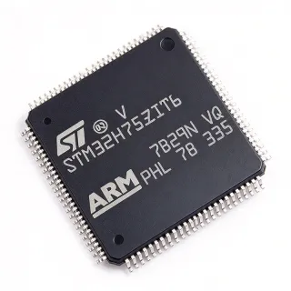
LPC1788FBD144 - ARM Cortex-M3 MCU 512KB Flash 144-LQFP | NXP
Артикул: LPC1788FBD144 ✓ Активен| Кол-во | Цена за ед. | Итого |
|---|---|---|
| 1 | $15.08 | $15,08 |
| 10 | $13.85 | $138,50 |
| 100 | $12.2 | $1.220,00 |
| 500 | $10.95 | $5.475,00 |
| 1.000 | $9.8 | $9.800,00 |
LPC1788FBD144 Обзор
A microcontroller (MCU) is a single-chip computer that integrates a CPU core, memory, and programmable peripherals. The Cortex-M3 is a 32-bit RISC processor core designed by ARM for deterministic, low-latency embedded applications. It sits in the broader hierarchy of microcontrollers -> embedded processors -> semiconductors. LDOs themselves are voltage regulators, but in this case LPC1788FBD144 is a microcontroller, not an LDO - clarification is important because the LPC17xx family is sometimes confused with the TPS7A4701 LDO family due to similar prefix letters.
Key features of the LPC1788FBD144 include up to 120 MHz CPU clock, 512 KB on-chip flash program memory, 96 KB SRAM, an 8-channel DMA controller, an external memory controller (EMC), USB 2.0 full-speed Device/Host/OTG, 10/100 Ethernet MAC, an LCD controller supporting TFT panels up to 1024x768, CAN, I2C, I2S, SPI, UART, 12-bit ADC, 10-bit DAC, PWM, and a Real-Time Clock (RTC). Per the NXP product page summary, the part is supplied from a 2.4 V to 3.6 V rail and integrates an Ethernet MAC and USB PHY on chip.
The LPC1788FBD144 uses an ARM Cortex-M3 core with a 3-stage pipeline, hardware single-cycle multiply, and Tail-Chaining interrupt controller that reduces interrupt latency. The 96 KB SRAM is split between general use and SRAM bytes, with the bytes portion (typically 4 KB) retained in low-power modes for RTC backup. The Ethernet MAC supports MII/RMII interfaces to an external PHY, while the EMC allows expansion with external SRAM, NOR flash, or SDRAM.
Typical applications for the LPC1788FBD144 include industrial HMI panels with TFT displays, building automation gateways, point-of-sale terminals, embedded data loggers, and USB/Ethernet-connected embedded controllers. The combination of large SRAM, integrated Ethernet and USB, and an LCD controller makes it particularly suited to graphics-rich industrial products.
Designers should note that the 144-LQFP package has a relatively large 20x20 mm footprint and 0.5 mm pitch, requiring careful PCB layout for the high-speed Ethernet MII/RMII traces. Power supply decoupling is critical at the 3.3 V main and 1.2 V core rails, and the EMC bus must be length-matched for SDRAM. This page synthesizes distributor pricing, drop-in NXP family alternatives, and practical design notes that are not aggregated in the manufacturer datasheet.
Аналоги без доработки для LPC1788FBD144 — тот же корпус, pin-to-pin совместимость. Компоненты в других корпусах, требующие переработки PCB, исключены.
Варианты в этой серии
Модели той же серии, совместимые без доработки с LPC1788FBD144 (тот же форм-фактор и посадочное место) — отличается по ADC, Ethernet, Package, SRAM, LCD Controller.
Инструмент быстрого сравнения — выберите альтернативные компоненты для сравнения бок о бок:
LPC1778FBD144
✅ Прямая замена📋 Справочный аналог (нет в каталоге)
LPC1768FBD144
✅ Прямая замена📋 Справочный аналог (нет в каталоге)
LPC4088FBD144
✅ Прямая замена✓ В наличии
$9.45 / шт.
Открыть даташит →LPC1788FBD208
✅ Прямая замена📋 Справочный аналог (нет в каталоге)
LPC1786FBD144
✅ Прямая замена📋 Справочный аналог (нет в каталоге)
LPC1788FBD144 Максимальные параметры и электрические характеристики
| Core | ARM Cortex-M3 32-bit |
| Maximum CPU Clock | 120 MHz |
| Program Flash | 512 KB (512K x 8) |
| SRAM | 96 KB |
| Напряжение питания | 2.4 V to 3.6 V |
| I/O Pins | 119 |
| Корпус | LQFP-144 (20x20 mm, 0.5 mm pitch) |
| Ethernet | 10/100 MAC (MII/RMII) |
| USB | USB 2.0 FS Device/Host/OTG |
| LCD Controller | Yes (up to 1024x768 TFT) |
| External Memory Controller (EMC) | Yes (SRAM/NOR/SDRAM) |
| ADC | 12-bit |
| DAC | 10-bit |
| Тип монтажа | Surface Mount |
| Статус RoHS | Compliant |
Руководство по цоколевке LPC1788FBD144 в корпусе lqfp-144 (20x20 mm, 0.5 mm pitch)
Цоколевка для LPC1788FBD144 (корпус lqfp-144 (20x20 mm, 0.5 mm pitch)). Эта цифровая ИС включает выводы GPIO, интерфейсы связи (UART, SPI, I2C) и выводы питания. Обратитесь к техническому описанию производителя для альтернативных функций выводов и вариантов конфигурации. Необходимо для проектирования встраиваемых систем и трассировки печатных плат.
Нет подробных данных о распиновке для LPC1788FBD144.
Обратитесь к даташиту для полной конфигурации выводов.
Типичное применение
LPC1788FBD144 подходит для 6 применениеs: Industrial HMI with TFT Display, Building Automation Gateway, Point-of-Sale Terminal, Embedded Data Logger with Ethernet, USB/Ethernet Connected Embedded Controller, Automotive Infotainment Sub-display Controller.
Industrial HMI with TFT Display
The LPC1788FBD144 is well suited for industrial HMI panels that drive a TFT LCD and connect to a factory network. Its integrated LCD controller supports panels up to 1024x768, removing the need for an external graphics controller and saving BOM cost. The on-chip 10/100 Ethernet MAC allows direct connection to an external PHY for Modbus TCP or PROFINET-style communication, while the 96 KB SRAM and 512 KB flash can hold a graphics library plus a real-time GUI stack. Power dissipation stays low because the LCD bus and Ethernet share internal DMA channels rather than burning CPU cycles.
Рекомендуется
Building Automation Gateway
For building automation gateways that aggregate KNX, Modbus, or BACnet traffic onto Ethernet, the LPC1788FBD144 provides the right mix of UARTs, CAN, SPI, I2C, and Ethernet. The 512 KB flash is large enough to hold a TCP/IP stack plus application logic, and the EMC controller allows SDRAM expansion if more RAM is needed. The 120 MHz Cortex-M3 core handles encryption for secure commissioning with low jitter thanks to the deterministic interrupt controller.
Рекомендуется
Point-of-Sale Terminal
POS terminals benefit from the LPC1788FBD144's USB Device/Host/OTG controller, which supports peripherals such as barcode scanners, receipt printers, and customer displays. The Ethernet MAC enables IP-based payment terminal connectivity, while the LCD controller drives the operator display. The 96 KB SRAM is sufficient for transaction buffering, and the external memory controller can interface to SDRAM for customer-facing graphics. Low power modes keep idle current low when the terminal is between transactions.
Рекомендуется
Embedded Data Logger with Ethernet
Industrial data loggers that record sensor data and stream it over Ethernet or upload to USB flash drives are a strong fit for the LPC1788FBD144. The Cortex-M3 at 120 MHz can sample multiple ADC channels while servicing the Ethernet stack. The 512 KB flash holds a small file system plus firmware, and the 96 KB SRAM is enough for buffering. USB Host mode supports external mass storage for offline data transfer.
Рекомендуется
USB/Ethernet Connected Embedded Controller
General-purpose embedded controllers that need both USB and Ethernet connectivity are a primary use case for the LPC1788FBD144. The on-chip USB 2.0 FS Device/Host/OTG port and 10/100 Ethernet MAC remove the need for an external bridge chip. The 119 GPIO plus the LCD controller mean a single chip can drive a panel, talk to a PC over USB, and connect to a network without extra silicon.
Рекомендуется
Automotive Infotainment Sub-display Controller
Sub-display controllers in automotive infotainment clusters can use the LPC1788FBD144 to drive small TFT panels and communicate with the head unit over CAN or Ethernet. The LCD controller handles graphics, the CAN interface links to the vehicle bus, and the EMC controller can attach external SDRAM for richer graphics content. Note that this part is not AEC-Q100 qualified; designs requiring full automotive qualification should evaluate the LPC1788FBD144-Q1 or another qualified part.
Рекомендуется
Сводка рекомендуемых товаров
Справочные инженерные данные для LPC1788FBD144 — сравнение, рекомендации по проектированию и информация о соответствии.
Руководство по выбору
Сравнение с аналогами
| Параметр | Этот товар | LPC1778FBD144 | LPC1768FBD144 | LPC4088FBD144 | LPC1786FBD144 | LPC1788FBD208 |
|---|---|---|---|---|---|---|
| Brand | NXP Semiconductors | NXP Semiconductors | NXP Semiconductors | NXP Semiconductors | NXP Semiconductors | NXP Semiconductors |
| Package | LQFP-144 (20x20 mm) | LQFP-144 (20x20 mm) - same | LQFP-144 (20x20 mm) - same | LQFP-144 (20x20 mm) - same | LQFP-144 (20x20 mm) - same | LQFP-208 (28x28 mm) |
| Core | Cortex-M3 120 MHz | Cortex-M3 120 MHz | Cortex-M3 100 MHz | Cortex-M4 with FPU 120 MHz | Cortex-M3 120 MHz | Cortex-M3 120 MHz |
| Flash | 512 KB | 512 KB | 512 KB | 512 KB | 256 KB | 512 KB |
| SRAM | 96 KB | 96 KB | 64 KB | 96 KB | 96 KB | 96 KB |
| LCD Controller | Yes (up to 1024x768) | Yes | No | Yes | Yes | Yes |
| Ethernet | 10/100 MAC (MII/RMII) | 10/100 MAC | 10/100 MAC | 10/100 MAC | 10/100 MAC | 10/100 MAC |
| Supply Voltage | 2.4 V to 3.6 V | 2.4 V to 3.6 V | 2.4 V to 3.6 V | 2.4 V to 3.6 V | 2.4 V to 3.6 V | 2.4 V to 3.6 V |
Ключевые отличия
- Highest flash density in the LPC17xx LQFP-144 family (против LPC1786FBD144)
- Larger SRAM than the LPC1768 predecessor (против LPC1768FBD144)
- ARM Cortex-M4 upgrade path on the same footprint (против LPC4088FBD144)
- Integrated Ethernet and USB reduces BOM (против LPC1778FBD144)
Заметки по проектированию
The LPC1788FBD144 requires a clean 3.3 V rail capable of supplying up to ~150 mA peak for the core plus peripheral current. Place a 10 uF bulk capacitor and a 100 nF decoupling capacitor close to each VDD/VDDA pin pair. The internal 1.2 V regulator needs its own 10 uF + 100 nF on the VDDREG pin. Avoid switching the main 3.3 V rail on/off rapidly because the POR circuit can mis-trigger.
The LQFP-144 package has a 0.5 mm pitch that demands careful PCB layout. Use 0.2 mm/8 mil trace width with 0.2 mm spacing, length-matched SDRAM data/address lines if the EMC is in use, and a continuous ground plane under the part. Place the external Ethernet PHY within 50 mm of the MAC pins to keep MII/RMII traces short. The 20x20 mm body is large enough to allow easy fan-out on a 4-layer PCB.
The Ethernet MII/RMII traces must be 50 ohm controlled-impedance with matched length between clock and data. The USB DP/DM traces must be 90 ohm differential impedance with no stubs. Place the ESD protection array within 3 mm of the USB connector. For LCD signals, route the upper data bits in a bus group and length-match within 2 mm to avoid skew with the LCD clock.
Common mistakes with the LPC1788FBD144 include forgetting to configure the PLL before raising the CPU clock above 24 MHz, leaving the boot pins in the wrong state so the part enters ISP mode unintentionally, omitting the 32 kHz crystal on the RTC oscillator (which disables the RTC and the bytes SRAM retention), and stacking too many peripherals on the same DMA channel. Always confirm the boot pin configuration in the system_LPC17xx.c startup file.
Информация о соответствии
RoHS compliant per NXP product page. Not AEC-Q100 qualified - automotive designs should evaluate LPC1788FBD144-Q1 or other AEC-Q100 qualified parts.