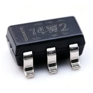
OPA378AIDBV - Zero-Drift 900kHz RRIO Op Amp | TI
Артикул: OPA378AIDBV ✓ Активен| Кол-во | Цена за ед. | Итого |
|---|---|---|
| 1 | $1.27 | $1,27 |
| 10 | $1.14 | $11,40 |
| 100 | $1.01 | $101,00 |
| 500 | $0.89 | $445,00 |
| 1.000 | $0.78 | $780,00 |
OPA378AIDBV Обзор
A zero-drift operational amplifier (also called a chopper-stabilized or auto-calibrated amplifier) is a precision amplifier topology that uses internal switching and correction to continuously null its input offset voltage, eliminating the 1/f (flicker) noise and offset drift that limit DC accuracy in conventional CMOS or bipolar op amps. The OPA378 belongs to the broader family of operational amplifiers -> precision amplifiers -> amplifiers -> analog signal-chain ICs -> semiconductor devices. This category is critical whenever a circuit needs to amplify or buffer microvolt-level DC signals without drift across temperature.
Key specifications include a 900 kHz gain bandwidth product (GBW), 2.5 V/us typical slew rate, RRIO operation from a 2.7 V to 5.5 V single supply, 150 uA maximum quiescent current, and an input bias current of 200 pA. The combination of low offset (20 uV), near-zero drift (0.1 uV/°C), low noise, and micropower consumption enables high DC accuracy in battery-powered and bridge-sensor applications without auto-zero cycle latency.
Internally, the OPA378 uses a proprietary auto-calibration technique that continuously samples and corrects the input stage offset, achieving picoampere-level effective input bias drift over time and temperature. Rail-to-rail input and output stages allow the part to operate with signals that approach either supply rail, maximizing dynamic range in low-voltage single-supply systems. The 5-pin SOT-23 package is footprint-compatible with industry-standard SOT-23-5 single-channel op amps, supporting PCB-level drop-in replacement.
Typical applications include precision strain-gauge and thermocouple signal conditioning, transducer excitation amplifiers, battery-powered sensor front-ends, medical instrumentation, handheld test equipment, and current-sense amplifiers. Designers select the OPA378 specifically when sub-100 uV DC error and sub-uV/°C drift are required in systems that cannot tolerate the noise and quiescent current of legacy precision op amps.
When designing with this device, ensure the input common-mode range includes the expected signal excursion, since RRIO operation only guarantees linear behavior within the specified input voltage range. Use low-impedance drive sources or a series input resistor to attenuate switching transients from the chopper front-end, and add a small RC filter at the output if any residual clock feedthrough is unacceptable in the target application.
This page synthesizes distributor pricing, drop-in alternatives, and practical design notes not found in the manufacturer datasheet, giving engineers an actionable reference for sourcing and second-sourcing decisions.
Аналоги без доработки для OPA378AIDBV — тот же корпус, pin-to-pin совместимость. Компоненты в других корпусах, требующие переработки PCB, исключены.
Варианты в этой серии
Модели той же серии, совместимые без доработки с OPA378AIDBV (тот же форм-фактор и посадочное место) — отличается по MSL Level, Number of Channels, Operating Temperature Range, Package.
Инструмент быстрого сравнения — выберите альтернативные компоненты для сравнения бок о бок:
OPA378AIDBVR
✅ Прямая замена📋 Справочный аналог (нет в каталоге)
OPA2378AIDGKR
✅ Прямая замена ⚠️ Характеристики не проверены📋 Справочный аналог (нет в каталоге)
MAX44250AUT+T
✅ Прямая замена📋 Справочный аналог (нет в каталоге)
MAX9914EXK+T
✅ Прямая замена📋 Справочный аналог (нет в каталоге)
LMV841MGX/NOPB
✅ Прямая замена✓ В наличии
$0.78 / шт.
Открыть даташит →OPA378AIDBV Максимальные параметры и электрические характеристики
| Manufacturer | Texas Instruments |
| Product Type | Zero-Drift Precision Operational Amplifier |
| Number of Channels | 1 |
| Gain Bandwidth Product (GBW) | 900 kHz |
| Slew Rate | 2.5 V/us (typical) |
| Input Offset Voltage (Vos) | 20 uV (maximum) |
| Offset Voltage Drift (dVos/dT) | 0.1 uV/°C |
| Quiescent Current (Iq) | 150 uA (maximum) |
| Input Bias Current (Ib) | 200 pA |
| Supply Voltage Range (Vs) | 2.7 V to 5.5 V (single supply) |
| Input/Output Type | Rail-to-Rail Input and Output (RRIO) |
| Диапазон рабочих температур | -40°C to +125°C |
| Корпус | SOT-23-5 (DBV) |
| Тип монтажа | Surface Mount |
| Уровень MSL | 1 (unlimited) |
| Статус RoHS | Compliant |
| AEC-Q100 Qualified | No (industrial grade only) |
Конфигурация выводов OPA378AIDBV
| Контакт 1 | NC / Offset Trim — No-connect (offset trim pin left floating for standard use) |
| Контакт 2 | -In — Inverting input |
| Контакт 3 | +In — Non-inverting input |
| Контакт 4 | V- / GND — Negative supply (ground for single supply) |
| Контакт 5 | V+ — Positive supply (2.7 V to 5.5 V) |
Типичное применение
OPA378AIDBV подходит для 6 применениеs: Strain-Gauge / Load-Cell Signal Conditioning, Thermocouple / Cold-Junction Compensation, Battery-Powered Sensor Front-End, Medical Instrumentation Amplifier, Precision Current-Shunt Amplifier, Handheld Test & Measurement Equipment.
Strain-Gauge / Load-Cell Signal Conditioning
The OPA378AIDBV's 20 uV maximum input offset voltage and 0.1 uV/°C drift make it ideal for strain-gauge bridge amplifiers where microvolt-level differential signals must be amplified without thermal drift over the -40°C to +125°C range. Placed in the first gain stage with a fixed gain of 100, the part converts a full-scale bridge output of 1 mV/V to a 10 mV signal with sub-50 uV total error, eliminating the need for periodic system recalibration.
Рекомендуется
Thermocouple / Cold-Junction Compensation
For thermocouple front-ends measuring microvolt-per-degree Celsius signals, the OPA378AIDBV's zero-drift architecture and 200 pA input bias current reject 1/f noise and thermal EMF buildup at the thermocouple junction. Used as a low-noise front-end with a gain of 50-100 followed by a precision ADC, the part achieves better than 0.1°C measurement repeatability across the K-type thermocouple range (-200°C to +1372°C) without chopper feedthrough artefacts.
Рекомендуется
Battery-Powered Sensor Front-End
The OPA378AIDBV's 150 uA maximum quiescent current and 2.7 V-5.5 V supply range make it ideal for battery-powered IoT and portable sensor nodes where every microwatt of bias current matters. Combined with rail-to-rail I/O for maximum dynamic range at low supply voltages, the part delivers precision DC amplification for current-sense, voltage-sense, or analog-output sensors while preserving battery life for multi-year deployments.
Рекомендуется
Medical Instrumentation Amplifier
In ECG, EEG, and bio-impedance front-ends, the OPA378AIDBV's 20 uV Vos and 0.1 uV/°C drift ensure that millivolt-level bioelectric signals are amplified faithfully across patient body temperature variations and ambient shifts. Used as the input stage of a three-op-amp instrumentation amplifier with 0.1% gain-set resistors, the part supports medical-grade measurement with sub-mV error budgets in wearable and diagnostic platforms.
Рекомендуется
Precision Current-Shunt Amplifier
For high-side or low-side current-sense circuits reading across a 10-100 mΩ shunt, the OPA378AIDBV's low Vos drift across temperature eliminates current measurement error when the surrounding power electronics heat up. Used with a fixed gain of 20-50 to convert a 0-100 mV shunt signal to a 0-5 V ADC input, the zero-drift topology avoids the 0.3-3 uV/°C drift inherent in standard op amps which would otherwise demand temperature calibration.
Рекомендуется
Handheld Test & Measurement Equipment
In portable multimeters, low-bandwidth oscilloscopes, and signal calibrators, the OPA378AIDBV's combination of low offset (20 uV), high GBW (900 kHz), and rail-to-rail I/O enables precise buffer and gain stages that operate from a single Li-ion cell. The 5-pin SOT-23 package minimizes PCB area in handheld enclosures, while the 150 uA quiescent current extends battery runtime between charges.
Рекомендуется
Сводка рекомендуемых товаров
Справочные инженерные данные для OPA378AIDBV — сравнение, рекомендации по проектированию и информация о соответствии.
Руководство по выбору
Сравнение с аналогами
| Параметр | Этот товар | OPA378AIDBVR | OPA2378AIDGKR | MAX44250AUT+T | MAX9914EXK+T | LMV841MGX/NOPB |
|---|---|---|---|---|---|---|
| Brand | Texas Instruments | Texas Instruments | Texas Instruments | Analog Devices (Maxim) | Analog Devices (Maxim) | Texas Instruments |
| Package | SOT-23-5 (DBV) | SOT-23-5 (DBV) | MSOP-8 (DGK) - dual, different footprint | SOT-23-5 | SC-70-5 (slightly smaller) | SC-70-5 (MGX) |
| Gain Bandwidth Product | 900 kHz | 900 kHz | 900 kHz | 10 MHz (much higher) | ~500 kHz | 4.5 MHz |
| Quiescent Current (max) | 150 uA | 150 uA | 150 uA per channel | 1.2 mA (higher) | ~200 uA | 1.5 mA |
| Supply Voltage Range | 2.7 V to 5.5 V | 2.7 V to 5.5 V | 2.7 V to 5.5 V | 2.7 V to 5.5 V | 2.7 V to 5.5 V | 2.7 V to 5.5 V |
| Rail-to-Rail I/O | Yes (RRIO) | Yes | Yes | Yes | Yes | Output only (no RRIO) |
Ключевые отличия
- Sub-uV/°C drift eliminates thermal calibration (против LMV841MGX/NOPB)
- Single-supply RRIO operation maximizes dynamic range at low Vs (против MAX9914EXK+T)
- Pin-compatible drop-in versus the dual OPA2378 sibling for designs needing second-source (против OPA2378AIDGKR)
Заметки по проектированию
Estimated: source impedance above 10 kΩ injected into the +In/-In pins can interact with the auto-calibration switches and amplify residual clock feedthrough as a DC offset error. For a strain-gauge bridge with 1 kΩ output impedance this is rarely a problem, but for thermocouples with 10 kΩ source resistance add a unity-gain buffer at the input. The TI OPA378 datasheet (Rev. D) recommends keeping source impedance below 1 kΩ for lowest drift, otherwise add a series RC filter (10 kΩ + 1 nF) to roll off chopper transients.
Estimated: the SOT-23-5 thermal pad is on pin 4 (V-/GND), so use a small copper pour connected to ground to improve thermal dissipation when operating near 150 uA quiescent at +125°C ambient. Place a 0.1 uF X7R bypass capacitor within 2 mm of the V+ pin and a 10 uF tantalum or ceramic bulk capacitor at the supply node; keep input traces short and parallel to reduce loop area and avoid sourcing noise into the high-impedance inputs. Ground-plane stitching every 5 mm under the input traces lowers stray pickup in RF or switching environments.
For precision designs, route the inverting and non-inverting inputs as a matched differential pair on the same layer with constant 0.2-0.3 mm spacing to reject thermal and capacitive gradients. Place any gain-setting feedback resistors immediately next to the inverting input and connect their far ends to a clean ground pour or to the output pin with minimal trace length. Apply a guard ring driven by the same input signal around high-impedance traces to reduce leakage currents from contaminated PCB surfaces, particularly in presence of flux residues or humidity.
Информация о соответствии
RoHS compliant per TI product page. Not AEC-Q100 qualified - industrial temperature grade only (-40°C to +125°C). Lead-free and halogen-free per TI's environmental compliance markings.