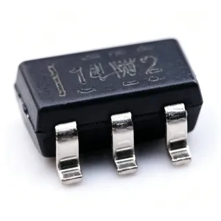
TLV316QDBVRQ1 - 10MHz RRIO Op Amp, AEC-Q100, SOT-23-5 | TI
Артикул: TLV316QDBVRQ1 ✓ Активен| Кол-во | Цена за ед. | Итого |
|---|---|---|
| 1 | $1.42 | $1,42 |
| 10 | $1.28 | $12,80 |
| 100 | $1.05 | $105,00 |
| 500 | $0.89 | $445,00 |
| 1.000 | $0.76 | $760,00 |
| 3.000 | $0.62 | $1.860,00 |
TLV316QDBVRQ1 Обзор
An operational amplifier (op amp) is a high-gain DC-coupled differential amplifier that uses external feedback to set its closed-loop behavior - gain, bandwidth, input impedance, and output impedance. Op amps form the fundamental building blocks of analog signal conditioning: inverting/non-inverting amplifiers, active filters, integrators, comparators, transimpedance amplifiers, and current/voltage buffers. Within the broader signal-chain taxonomy, general-purpose CMOS op amps sit between low-power chopper/zero-drink amplifiers and high-speed current-feedback op amps, optimized for portable, battery-powered, and automotive sensor-interface applications.
Key features of the TLV316QDBVRQ1 include rail-to-rail input common-mode range that includes both supply rails, rail-to-rail output swing within tens of millivolts of either rail, 1.8 V minimum supply enabling direct Li-ion/cell operation, 400 µA typical quiescent current per channel, and 12 nV/√Hz voltage noise density at 1 kHz. AEC-Q100 Grade 1 qualification (-40 °C to +125 °C ambient), HBM ESD Class 3A, and CDM ESD Class C5 ratings make it suitable for under-hood and cabin automotive modules.
Internally the device uses a CMOS input stage that supports true rail-to-rail common-mode operation without the crossover-distortion artifacts of legacy bipolar RRIO parts. The 10-MHz gain-bandwidth product combined with 6 V/µs typical slew rate provides sufficient speed for moderate-bandwidth sensor conditioning, audio pre-amplification, and active filter stages at audio frequencies.
Typical applications include automotive sensor signal conditioning (current-shunt monitors, thermistor bridges, pressure/temperature transducers), body and chassis ECUs, infotainment audio pre-amplifiers, low-side/battery current sensing, and portable/mobile precision buffers. The wide supply range also supports industrial 3.3 V and 5 V PLC analog input modules.
When designing with this op amp, place a 0.1 µF decoupling capacitor within a few millimeters of the supply pin, use a feedback network that keeps total gain above the minimum stable gain of 1 V/V (unity), and observe the input common-mode range - although RRIO, the input stage shifts distortion performance near the rails, so biasing the input mid-supply preserves linearity.
This page synthesizes distributor pricing, drop-in pin-compatible alternatives, and practical PCB design notes that go beyond the manufacturer datasheet to accelerate automotive and industrial analog front-end design decisions.
Аналоги без доработки для TLV316QDBVRQ1 — тот же корпус, pin-to-pin совместимость. Компоненты в других корпусах, требующие переработки PCB, исключены.
Инструмент быстрого сравнения — выберите альтернативные компоненты для сравнения бок о бок:
TLV316QDBVTQ1
✅ Прямая замена📋 Справочный аналог (нет в каталоге)
TLV316IDBVR
✅ Прямая замена📋 Справочный аналог (нет в каталоге)
TLV9061IDBVR
✅ Прямая замена📋 Справочный аналог (нет в каталоге)
OPA316IDBVR
✅ Прямая замена📋 Справочный аналог (нет в каталоге)
TLV9061QDBVRQ1
✅ Прямая замена📋 Справочный аналог (нет в каталоге)
TLV316QDBVRQ1 Максимальные параметры и электрические характеристики
| Amplifier Type | General-purpose, single-channel, RRIO CMOS op amp |
| Number of Channels | 1 |
| Gain-Bandwidth Product (GBW) | 10 MHz |
| Slew Rate | 6 V/µs (typical) |
| Supply Voltage Range (Single Supply) | 1.8 V to 5.5 V |
| Supply Voltage Range (Dual Supply) | ±0.9 V to ±2.75 V |
| Quiescent Current (per channel) | 400 µA (typical) |
| Input Voltage Noise Density | 12 nV/√Hz at 1 kHz |
| Input Common-Mode Range | Rail-to-Rail (includes both supply rails) |
| Output Swing | Rail-to-Rail (RRIO) |
| Диапазон рабочих температур | -40 °C to +125 °C (AEC-Q100 Grade 1) |
| ESD - HBM | Class 3A |
| ESD - CDM | Class C5 |
| Automotive Qualification | AEC-Q100 Grade 1 |
| Корпус | SOT-23-5 (DBV) |
| Тип монтажа | Surface Mount |
| Статус RoHS | Compliant |
| Lead-Free | Yes |
Конфигурация выводов TLV316QDBVRQ1
| Контакт 1 | NC — Not connected (per datasheet) |
| Контакт 2 | IN- — Inverting input |
| Контакт 3 | IN+ — Non-inverting input |
| Контакт 4 | V- — Negative supply (ground for single-supply operation) |
| Контакт 5 | OUT — Output |
Типичное применение
TLV316QDBVRQ1 подходит для 6 применениеs: Automotive Sensor Signal Conditioning, Body and Chassis ECU Analog Inputs, Infotainment Audio Pre-Amplifier, Battery Current Sensing (Low-Side), Active Filter Building Blocks (Sallen-Key, MFB), Portable / Battery-Powered Precision Buffer.
Automotive Sensor Signal Conditioning
The TLV316QDBVRQ1's 10 MHz GBW, 12 nV/√Hz input noise, and AEC-Q100 Grade 1 qualification make it a strong fit for automotive sensor front ends such as thermistor bridges, RTD interfaces, pressure transducers, and Hall-effect current sensors. Its rail-to-rail input and output allow direct connection to single-supply 5 V or 3.3 V ADCs without level shifting, maximizing dynamic range in low-voltage signal chains. The wide -40 °C to +125 °C ambient range covers under-hood and cabin placement, while HBM ESD Class 3A and CDM ESD Class C5 protect against automotive ESD events on the connector. Compared to legacy bipolar op amps, the CMOS RRIO input eliminates crossover distortion that would otherwise corrupt low-frequency sensor measurements near the rails.
Рекомендуется
Body and Chassis ECU Analog Inputs
Body control modules and chassis ECUs monitor multiple analog inputs including battery voltage, current shunts, door-switch positions, and lighting feedback. The TLV316QDBVRQ1's 1.8 V to 5.5 V supply range allows direct operation from a 12 V automotive rail that is regulated down to 5 V or 3.3 V locally, while the 10 MHz GBW provides ample closed-loop bandwidth for anti-aliasing active stages. The 400 µA quiescent current per channel is acceptable for always-on modules where the ECU remains awake for CAN/LIN polling. AEC-Q100 Grade 1 qualification simplifies PPAP documentation and ensures long-term reliability over the automotive service life. The SOT-23-5 footprint supports high-density multi-channel input conditioning on small PCBAs.
Рекомендуется
Infotainment Audio Pre-Amplifier
The TLV316QDBVRQ1 delivers sufficient bandwidth and noise performance for audio pre-amplifier stages in head units and rear-seat entertainment systems. Its 10 MHz GBW supports the full 20 Hz–20 kHz audio band with substantial headroom for active filter stages, while the 12 nV/√Hz voltage noise density at 1 kHz keeps the noise floor well below typical audio DAC output levels. Rail-to-rail output swing maximizes usable dynamic range on a 3.3 V or 5 V supply. The AEC-Q100 qualification ensures reliable operation in the thermally challenging dashboard environment, and the SOT-23-5 package fits easily alongside audio DACs and Class-D amplifier feedback networks. Compared to legacy bipolar audio op amps, the CMOS input stage avoids the input bias-current drift that would otherwise couple into high-impedance source signals.
Рекомендуется
Battery Current Sensing (Low-Side)
Low-side current sensing with a shunt resistor is a common technique for monitoring battery drain in automotive body modules and portable electronics. The TLV316QDBVRQ1's rail-to-rail input common-mode range allows the op amp to sense voltages very close to ground, which is ideal for low-side shunt configurations where the shunt voltage is small (tens of millivolts). Its 12 nV/√Hz noise floor ensures the small shunt voltage is not buried in amplifier noise, and the 10 MHz GBW enables wideband current monitoring for fast transient events such as cranking or in-rush. The 400 µA quiescent current is acceptable for always-on battery monitoring, and AEC-Q100 Grade 1 qualification supports direct automotive deployment. Use a gain-setting resistor network to amplify the shunt drop to a usable ADC input range.
Рекомендуется
Active Filter Building Blocks (Sallen-Key, MFB)
The TLV316QDBVRQ1's 10 MHz gain-bandwidth product and 6 V/µs slew rate make it well-suited for active filter implementations such as Sallen-Key and multiple-feedback (MFB) low-pass, high-pass, and band-pass topologies used in sensor signal conditioning and anti-aliasing. Its rail-to-rail input and output allow the filter to operate at supply-rail extremes without distortion artifacts, maximizing dynamic range on low-voltage rails. The 12 nV/√Hz input noise keeps the filter's noise contribution low for moderate-Q designs. Automotive Grade 1 qualification and the SOT-23-5 footprint fit compact industrial and automotive filter PCBs. The op amp's unity-gain stability simplifies buffer/integrator stages that often sit alongside filter networks.
Рекомендуется
Portable / Battery-Powered Precision Buffer
Portable instrumentation, handheld medical peripherals, and IoT sensor nodes often require a low-voltage precision buffer that operates directly from a Li-ion cell or two AAA batteries. The TLV316QDBVRQ1's 1.8 V minimum supply voltage allows direct operation down to a nearly discharged single Li-ion cell, while its 400 µA quiescent current balances speed and power for always-on buffering. The 10 MHz GBW comfortably handles the bandwidth requirements of typical sensor and transducer interfaces, and the rail-to-rail input/output preserves dynamic range on low supply voltages. The SOT-23-5 footprint fits miniature PCBs, and AEC-Q100 Grade 1 qualification provides headroom for harsh-environment portable devices. Pair it with a low-quiescent LDO for best noise performance in the analog signal chain.
Рекомендуется
Сводка рекомендуемых товаров
Справочные инженерные данные для TLV316QDBVRQ1 — сравнение, рекомендации по проектированию и информация о соответствии.
Руководство по выбору
Сравнение с аналогами
| Параметр | Этот товар | TLV316QDBVTQ1 | TLV316IDBVR | TLV9061IDBVR | OPA316IDBVR | TLV9061QDBVRQ1 |
|---|---|---|---|---|---|---|
| Brand | Texas Instruments | Texas Instruments | Texas Instruments | Texas Instruments | Texas Instruments | Texas Instruments |
| Package | SOT-23-5 (DBV) | SOT-23-5 (DBV) - same | SOT-23-5 (DBV) - same | SOT-23-5 (DBV) - same | SOT-23-5 (DBV) - same | SOT-23-5 (DBV) - same |
| Gain-Bandwidth Product | 10 MHz | 10 MHz | 10 MHz | 6.5 MHz | 10 MHz | 6.5 MHz |
| Supply Voltage Range | 1.8 V to 5.5 V | 1.8 V to 5.5 V | 1.8 V to 5.5 V | 1.8 V to 5.5 V | 1.8 V to 5.5 V | 1.8 V to 5.5 V |
| Quiescent Current (typ, per ch) | 400 µA | 400 µA | 400 µA | 538 µA | 400 µA | 538 µA |
| Input Voltage Noise (nV/√Hz at 1 kHz) | 12 | 12 | 12 | 10 | 11 | 10 |
| Rail-to-Rail I/O | Yes (input + output) | Yes | Yes | Yes | Yes | Yes |
| Automotive Grade (AEC-Q100) | Yes (Grade 1, -40 to +125 °C) | Yes (Grade 1) | No (industrial) | No (industrial) | No (industrial) | Yes (Grade 1) |
Ключевые отличия
- AEC-Q100 Grade 1 automotive qualification with full TI documentation (против TLV316IDBVR)
- Higher GBW (10 MHz) compared to the TLV9061 family at the same footprint (против TLV9061QDBVRQ1)
- Lower quiescent current than the TLV9061 family (против TLV9061IDBVR)
Заметки по проектированию
Place a 0.1 µF X7R/C0G ceramic decoupling capacitor within 5 mm of the V+ supply pin (pin 5 of the SOT-23-5 package) to suppress supply noise and prevent oscillation. Use a ground plane on the top or bottom layer and stitch vias around the input/output traces to minimize parasitic capacitance and reduce EMI pickup on sensitive analog nodes. Avoid routing digital signals (CAN, LIN, switching regulator nodes) directly under the op amp package, as switching transients can couple into the high-impedance input pins through the substrate.
Although the TLV316QDBVRQ1 is rail-to-rail at both input and output, the input stage shows higher distortion and Vos drift when the common-mode voltage is within ~200 mV of either supply rail. For precision applications, bias the input signal mid-supply (typically V+ / 2) to keep the input stage in its lowest-distortion region. Additionally, although the part is unity-gain stable, ensure the capacitive load on the output does not exceed datasheet limits - typically a few hundred pF directly at the output, or up to several nF when isolated with a small series resistor.
For low-noise sensor front-end designs, pair the TLV316QDBVRQ1 with a low-noise LDO such as the TPS7A4701RGWR (4.17 µVrms) on the analog supply rail. Use 1% metal-film or thin-film resistors in the feedback network to minimize gain error, and place the feedback components adjacent to the inverting input pin to keep parasitic trace capacitance small. For driving an ADC, add a small RC anti-aliasing filter at the op amp output, choosing the capacitor value to provide at least 10 dB attenuation at the sampling frequency while keeping the RC time constant well below the ADC acquisition window.
Информация о соответствии
AEC-Q100 Grade 1 qualified per TI TLV316-Q1 datasheet. HBM ESD Class 3A, CDM ESD Class C5. RoHS and REACH compliant. Lead-free and halogen-free per TI material declaration.