Texas Instruments

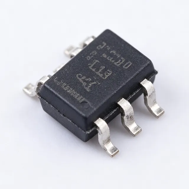
SN74AHC1G08-Q1 - Automotive 2-Input AND Gate SC-70-5 | TI

Артикул: SN74AHC1G08QDCKRQ1 ✓ Активен
В наличии Отправка в течение 1–3 рабочих дней
2 V to 5.5 V Vdss SC-70-5 (DCK) Package
От $0.09 USD / шт.
MOQ: 1 |
Цена обновлена: 2026-09-03
Оптовые цены
Кол-во Цена за ед. Итого
1 $0.32 $0,32
10 $0.26 $2,60
100 $0.16 $16,00
500 $0.12 $60,00
1.000 $0.09 $90,00
ℹ️ Все цены указаны в USD

SN74AHC1G08QDCKRQ1 Обзор

The Texas Instruments SN74AHC1G08-Q1 is an automotive-qualified single 2-input positive-AND gate that performs the Boolean function Y = A AND B in positive logic. Operating from a 2V to 5.5V supply, the device delivers a maximum propagation delay of 9 ns at 5V and comes in a 5-pin SC-70 (DCK) surface-mount package.

A single-gate logic IC integrates exactly one logic function - here an AND gate - in a tiny footprint, unlike traditional quad-gate devices such as the 74HC08. Single-gate devices sit within the broader CMOS logic IC family, under combinational logic, and are widely used for glue logic, signal gating, and enable generation in modern PCBs where board space is at a premium.

Key features include the AHC family's balanced CMOS architecture for low static power consumption, a wide 2V to 5.5V operating range supporting both 3.3V and 5V systems, and latch-up performance exceeding 250 mA per JESD 17. ESD protection exceeds 2000-V Human-Body Model, 200-V Machine Model, and 1000-V Charged-Device Model per TI datasheet. The -Q1 suffix denotes AEC-Q100 qualification for automotive applications.

The AHC technology provides TTL-compatible CMOS outputs with balanced drive and fast switching, while the unbuffered single-stage design keeps propagation delay tight and predictable across the operating range. Typical applications include automotive body electronics and cluster gating, industrial PLC I/O conditioning, and general-purpose enable/signal gating in mixed 3.3V/5V systems.

Design tip: keep unused input pins tied to VCC or GND, and place a 0.1uF decoupling capacitor close to the VCC pin to ensure clean switching edges and minimize ground bounce in automotive noise environments.

Аналоги без доработки для SN74AHC1G08QDCKRQ1 — тот же корпус, pin-to-pin совместимость. Компоненты в других корпусах, требующие переработки PCB, исключены.

Варианты в этой серии

Модели той же серии, совместимые без доработки с SN74AHC1G08QDCKRQ1 (тот же форм-фактор и посадочное место) — отличается по Logic Family, Logic Function, Output Type, Package, Supply Voltage Range.

Texas Instruments
Logic Family: LVC (Low-Voltage CMOS)
Logic Function: AND Gate
Output Type: Push-Pull
Сравнить с SN74AHC1G08QDCKRQ1 →

Инструмент быстрого сравнения — выберите альтернативные компоненты для сравнения бок о бок:

SN74AHC1G08DCKR

same die and pinout, standard industrial grade (not AEC-Q100 qualified)

📋 Справочный аналог (нет в каталоге)

SN74AHC1G08QDBVRQ1

same die and function, automotive grade, but SOT-23-5 footprint differs from SC-70-5 - requires PCB footprint change

📋 Справочный аналог (нет в каталоге)

74AHC1G08GV,125

cross-brand pin-compatible single 2-input AND gate, same SC-70-5 footprint, inputs overvoltage tolerant

📋 Справочный аналог (нет в каталоге)

74AHC1G08SE-7

Diodes Incorporated
AND Gate · 1 · 2 · AHC (Advanced High-speed CMOS) · 2.0 V to 5.5 V · 16 ns (typical at 5 V) · +/-8 mA · CMOS

✓ В наличии

$0.09 / шт.

Открыть даташит →

SN74HCS08QDYYRQ1

same function plus Schmitt-trigger inputs, but SOT-23-5 package - footprint change required

📋 Справочный аналог (нет в каталоге)

SN74AHC1G08QDCKRQ1 Максимальные параметры и электрические характеристики

Logic Function 2-Input Positive-AND Gate (Y = A AND B)
Number of Gates 1 (single gate)
Supply Voltage Range 2 V to 5.5 V
Max Propagation Delay 9 ns at 5 V
Logic Family AHC
Automotive Qualification AEC-Q100 (Q1)
Latch-Up Performance Exceeds 250 mA per JESD 17
ESD Protection (HBM) Exceeds 2000 V
ESD Protection (MM) Exceeds 200 V
ESD Protection (CDM) Exceeds 1000 V
Input Type Standard CMOS
Тип выхода Push-Pull CMOS
Корпус SC-70-5 (DCK)
Тип монтажа Surface Mount
Статус RoHS Compliant

Конфигурация выводов SN74AHC1G08QDCKRQ1

SC-70 Package Pinout Diagram SC-70 3-pin small outline transistor, JEDEC MO-003. 1 2 3 SC-70
Контакт 1 A — Input A
Контакт 2 GND — Ground
Контакт 3 B — Input B
Контакт 4 Y — Output (Y = A AND B)
Контакт 5 VCC — Power supply, 2V to 5.5V

Типичное применение

SN74AHC1G08QDCKRQ1 подходит для 6 применениеs: Automotive Body Electronics, Instrument Cluster Signal Gating, Industrial PLC I/O Conditioning, Mixed-Voltage Glue Logic, CAN and Communication Node Enable Logic, Battery-Managed Power System Gating.

🚗

Automotive Body Electronics

The SN74AHC1G08-Q1 gates switch inputs, door status signals, and interlock conditions in body control modules, where its AEC-Q100 qualification and latch-up performance exceeding 250 mA per JESD 17 address automotive robustness requirements. Its 2V to 5.5V supply range tolerates automotive 5V rail variation, and the 9 ns propagation delay at 5V adds negligible timing skew. The SC-70-5 package fits dense body-controller PCBs, allowing a single gate to be placed directly at the connector-side conditioning circuit rather than routing long traces to a multi-gate device.

📺

Instrument Cluster Signal Gating

In instrument clusters, the device combines warning enable signals and backlight interlocks with a 9 ns maximum delay at 5V, keeping timing deterministic across the cluster MCU's strobe schedule. AEC-Q100 qualification covers the extended automotive temperature environment behind the dashboard. Operating from the 5V cluster rail with balanced AHC CMOS drive, its push-pull output can directly drive indicator buffer inputs or LED driver enable pins. Low static power consumption keeps quiescent draw negligible in partially powered cluster states, supporting key-off battery drain budgets in modern vehicles.

🏭

Industrial PLC I/O Conditioning

The SN74AHC1G08-Q1 combines interlock and safety-enable signals in PLC digital input modules, where the 2V to 5.5V range supports both 3.3V MCU-side and 5V field-side rails on one board. The 9 ns propagation delay at 5V is far faster than PLC scan cycles, adding effectively zero latency to interlock chains. ESD protection exceeding 2000V HBM provides margin near field wiring, and the compact SC-70-5 package allows gating directly at terminal-block conditioning circuits. Standard CMOS inputs suit buffered, conditioned field signals from optocoupler outputs.

🧩

Mixed-Voltage Glue Logic

The wide 2V to 5.5V supply window makes the SN74AHC1G08-Q1 a natural glue-logic element between 3.3V and 5V domains, for example gating a 3.3V MCU chip-select with a 5V-domain power-good signal. Balanced AHC CMOS output drive provides full-rail swing at the supply it is powered from, and the single-gate format eliminates unused-gate inputs that multi-gate packages create. Place the gate at the domain boundary with local 0.1uF decoupling to keep switching edges clean and limit ground bounce between domains.

🌐

CAN and Communication Node Enable Logic

The device gates transceiver STB/EN pins with MCU wake signals in CAN and LIN nodes: its 9 ns delay ensures the transceiver mode transition happens within microseconds of the MCU decision, and AEC-Q100 qualification meets automotive network node requirements. SC-70-5 sizing lets the gate sit beside the TCAN-family transceiver on a dense node PCB. Low power consumption in standby supports the node's sleep-current budget, and the robust ESD ratings (over 2000V HBM) add margin in harsh in-vehicle EMC environments near connector routing.

⚡

Battery-Managed Power System Gating

In battery management and power-path circuits, the SN74AHC1G08-Q1 combines power-good outputs and charger fault flags into a single system-enable signal. Its push-pull CMOS output directly drives load-switch enable pins without external pull resistors, and the 2V to 5.5V range matches both battery-backed 3.3V supervision rails and 5V power rails. The gate's fast 9 ns response prevents glitched enables during fault sequencing. Pair with a supervisor or PMIC power-good output, and tie the gate VCC to the always-on rail so the enable stays defined through power transitions.

Сводка рекомендуемых товаров

SN74LVC1G17QDBVRQ1 Texas Instruments Используется в: Automotive Body Electronics TLIN821-Q1 Texas Instruments Используется в: Automotive Body Electronics TPS7A1601QDGNRQ1 Texas Instruments Используется в: Automotive Body Electronics TPS92691QPWPTQ1 Texas Instruments Используется в: Instrument Cluster Signal Gating TMP117-Q1 Cluster temperature monitoring Используется в: Instrument Cluster Signal Gating LM358QDRQ1 Texas Instruments Используется в: Instrument Cluster Signal Gating ISO7742QFDBQRQ1 Digital isolator feeding gated inputs Используется в: Industrial PLC I/O Conditioning SN65HVD3085EDR Texas Instruments Используется в: Industrial PLC I/O Conditioning LM393DR Texas Instruments Используется в: Industrial PLC I/O Conditioning SN74LVC1T45QDCKRQ1 Texas Instruments Используется в: Mixed-Voltage Glue Logic SN74AVC4T245PWR Texas Instruments Используется в: Mixed-Voltage Glue Logic, Mixed-Voltage Glue Logic TXS0102-Q1 Texas Instruments Используется в: Mixed-Voltage Glue Logic TCAN337G-Q1 Texas Instruments Используется в: CAN and Communication Node Enable Logic SN65HVD230QDRQ1 Texas Instruments Используется в: CAN and Communication Node Enable Logic ISO1050QDUBRQ1 Texas Instruments Используется в: CAN and Communication Node Enable Logic BQ76952Q-Q1 Texas Instruments Используется в: Battery-Managed Power System Gating TPS22997QRYZRQ1 Texas Instruments Используется в: Battery-Managed Power System Gating TPS7A8300QRGRRQ1 Low-noise rail for gated logic domain Используется в: Battery-Managed Power System Gating
What is the SN74AHC1G08-Q1?
The SN74AHC1G08-Q1 is an automotive-qualified single 2-input positive-AND gate from Texas Instruments. It performs the Boolean function Y = A AND B in positive logic, operates from a 2V to 5.5V supply, has a maximum propagation delay of 9 ns at 5V, and comes in a 5-pin SC-70 (DCK) package, per TI datasheet.
What is the operating voltage range of SN74AHC1G08-Q1?
The SN74AHC1G08-Q1 operates from a 2V to 5.5V supply, according to TI product data. This wide range supports both 3.3V and 5V logic systems and allows use in automotive 5V rails with tolerance for supply transients within the specified window.
Is SN74AHC1G08-Q1 suitable for automotive applications?
Yes, the -Q1 suffix indicates the device is qualified for automotive applications per TI. It meets AEC-Q100 requirements, offers latch-up performance exceeding 250 mA per JESD 17, and provides ESD protection beyond 2000V HBM, making it suitable for body electronics, clusters, and other in-vehicle logic gating.
What is the propagation delay of SN74AHC1G08-Q1?
The maximum propagation delay is 9 ns at 5V supply, per TI datasheet. Actual delay varies with supply voltage and load capacitance, decreasing at higher VCC and smaller loads. This makes the device fast enough for enable gating, chip-select shaping, and general glue logic in most automotive and industrial designs.
What is the difference between SN74AHC1G08-Q1 and SN74AHC1G08?
The SN74AHC1G08-Q1 is the automotive-grade version of the standard SN74AHC1G08. Both are single 2-input AND gates with identical 2V to 5.5V operation and 9 ns delay at 5V; the -Q1 variant adds AEC-Q100 automotive qualification and related manufacturing quality controls. Functionally they are interchangeable in non-automotive designs.
What is the best drop-in replacement for SN74AHC1G08-Q1?
The best drop-in same-package alternatives are the standard-grade TI SN74AHC1G08 (SC-70-5/DCK, identical pinout and specs but not automotive qualified) and cross-brand Nexperia 74AHC1G08GV in SOT-353/SC-88A, which shares the same SC-70-5 footprint and pinout. Verify pinout against the datasheet before production use.
Can Nexperia 74AHC1G08 replace TI SN74AHC1G08-Q1?
Functionally and physically, the Nexperia 74AHC1G08GV (SC-88A/SOT-353, same as SC-70-5) can replace the TI part in non-automotive applications, as both implement a single 2-input AND gate over similar voltage ranges. However, Nexperia automotive-qualified equivalent (74AHC1G08-Q100) should be selected for automotive builds to maintain qualification requirements.
SN74AHC1G08-Q1 vs SN74HCS08-Q1 - which should I choose?
Choose SN74AHC1G08-Q1 for standard CMOS inputs and lowest cost in clean signal environments. Choose SN74HCS08-Q1 when slow or noisy input edges need Schmitt-trigger inputs for hysteresis, per TI E2E forum guidance - though note package options differ, so footprint compatibility must be checked for drop-in use.
When should I choose SN74AHC1G08-Q1 over SN74LVC1G08?
Choose the AHC device when you need the full 2V to 5.5V operating range, robust automotive qualification heritage, and relaxed input edge requirements. Choose LVC-family parts when faster propagation delay (around 3-4 ns at 3.3V) and lower dynamic power at high toggle rates matter more than the wide supply window.
How much does SN74AHC1G08-Q1 cost?
As of 2026-08-29, SN74AHC1G08QDCKRQ1 pricing at distributors is approximately $0.32 at quantity 1, dropping to roughly $0.16 at 100 units and around $0.09 at 1000 pieces in tape-and-reel packaging. Check DigiKey, Mouser, or Octopart for live pricing and stock, as logic gate prices fluctuate with demand.
Where can I download the SN74AHC1G08-Q1 datasheet PDF?
The official SN74AHC1G08-Q1 datasheet PDF is available at https://www.ti.com/lit/ds/symlink/sn74ahc1g08-q1.pdf from Texas Instruments. This 8-page document contains the pinout, absolute maximum ratings, recommended operating conditions, switching characteristics, and SC-70 (DCK) package mechanical drawings.
What is the pinout of SN74AHC1G08-Q1 in SC-70-5?
In the 5-pin SC-70 (DCK) package, pin 1 is input A, pin 2 is GND, pin 3 is input B, pin 4 is output Y, and pin 5 is VCC, per TI datasheet. The compact 2.0 mm x 1.25 mm footprint enables dense single-gate placement near the signals being gated.
Is SN74AHC1G08-Q1 RoHS compliant?
Yes, the SN74AHC1G08QDCKRQ1 is RoHS compliant and lead-free, per TI product page and distributor listings. The device is surface mounted in the SC-70 package with matte-tin lead finish suitable for standard reflow soldering processes used in automotive and industrial assembly.
What are the key specifications of SN74AHC1G08-Q1 engineers should know?
Key specs: single 2-input positive-AND gate; 2V to 5.5V supply; 9 ns max propagation delay at 5V; AEC-Q100 automotive qualified; latch-up over 250 mA per JESD 17; ESD above 2000V HBM, 200V MM, 1000V CDM; 5-pin SC-70 (DCK) package. Source: TI SN74AHC1G08-Q1 datasheet.

Справочные инженерные данные для SN74AHC1G08QDCKRQ1 — сравнение, рекомендации по проектированию и информация о соответствии.

Руководство по выбору

Choose SN74AHC1G08QDCKRQ1 when you need an automotive-qualified single AND gate in the smallest footprint: the SC-70-5 DCK package saves board area over the DBV option while sharing the same die and 2V-5.5V range. Choose the standard SN74AHC1G08DCKR for non-automotive builds where cost matters more than AEC-Q100. Choose SN74AHC1G08QDBVRQ1 if your PCB is already laid out for SOT-23-5. Select Nexperia 74AHC1G08GV as a second source sharing the SC-70 footprint, verifying pinout order first. If input signals are slow or noisy, consider SN74HCS08-Q1 with Schmitt-trigger inputs instead, accepting the footprint change. For maximum speed at 3.3V, LVC-family gates are faster but sacrifice the wide supply window.

Сравнение с аналогами

Параметр Этот товар SN74AHC1G08DCKR 74AHC1G08GV,125 74AHC1G08SE-7 SN74AHC1G08QDBVRQ1
Package SC-70-5 (DCK) SC-70-5 (DCK) - same SOT-353/SC-88A - same footprint SOT-25 - same footprint SOT-23-5 (DBV) - different footprint
Brand Texas Instruments Texas Instruments Nexperia Diodes Incorporated Texas Instruments
Supply Voltage Range 2 V to 5.5 V 2 V to 5.5 V 2 V to 5.5 V 2 V to 5.5 V 2 V to 5.5 V
Logic Function 2-input AND 2-input AND 2-input AND 2-input AND 2-input AND
Automotive Grade (AEC-Q100) Yes (Q1) No No (standard grade) No Yes (Q1)

Ключевые отличия

  • AEC-Q100 automotive qualification (против SN74AHC1G08DCKR)
  • Smallest footprint with same die as DBV option (против SN74AHC1G08QDBVRQ1)
  • Wide 2V to 5.5V range versus fast LVC alternatives (против 74AHC1G08GV,125)

Заметки по проектированию

Place a 0.1uF ceramic decoupling capacitor within 2-3 mm of the VCC pin (pin 5) and route a short return to GND (pin 2). Although a single AND gate draws little dynamic current, fast output edges into capacitive loads cause supply transients that, without local decoupling, couple into neighboring analog circuitry on shared rails.

This is a standard CMOS input device - do not leave inputs A or B floating, as unterminated CMOS inputs float near threshold and cause oscillation and excess ICC. Tie unused conditions to VCC or GND. Do not drive inputs from slow RC ramps; use a Schmitt-trigger buffer such as SN74LVC1G17 if edges are noisy or slow.

Power dissipation is dominated by output load switching, not static CMOS current. With a 50 pF load toggling at low frequencies, dissipation (P = C*V^2*f) stays in the microwatt range at 5V, so no thermal management is needed in the SC-70-5 package. Only high-frequency clock gating above tens of MHz merits a dissipation check.

Информация о соответствии

RoHS
Compliant
REACH
Unknown
AEC-Q100
Без свинца
Без галогенов
Unknown
Конфликтные минералы
Unknown

AEC-Q100 qualified (Q1 suffix) per TI product page. RoHS compliant and lead-free per distributor listings.


Данные проверены: 2026-08-29 — данные проверены и курируются командой компонентной инженерии XAIPART

Похожие запросы

SN74AHC1G08-Q1 datasheet SN74AHC1G08QDCKRQ1 Texas Instruments SN74AHC1G08-Q1 SN74AHC1G08-Q1 vs SN74AHC1G08 74AHC1G08 equivalent Nexperia automotive single AND gate SC-70 SN74AHC1G08-Q1 pinout 2V to 5.5V AND gate automotive SN74AHC1G08QDCKRQ1 price SN74HCS08-Q1 vs SN74AHC1G08-Q1 what can replace SN74AHC1G08-Q1 AEC-Q100 logic gate glue logic automotive

Связанные компоненты & термины

Texas Instruments SN74AHC1G08-Q1 SN74AHC1G08QDCKRQ1 SN74AHC1G08DCKR 74AHC1G08GV Nexperia AND gate single-gate logic CMOS logic glue logic AEC-Q100 JESD 17 SC-70-5 SOT-23-5 ESD HBM latch-up automotive body electronics propagation delay RoHS
Похожие технические руководства
SN74AHC1G08-Q1 (SN74AHC1G08QDCKRQ1): автомобильный логический элемент 2И — характеристики, цоколевка, цены и аналоги
SN74AHC1G08-Q1: автомобильный одиночный логический элемент 2И от TI, 2–5,5 В, макс. задержка 9 нс при 5 В, SC-70-5, AEC-Q100. В наличии, от
6 мин чтения
Быстрый запрос цены (RFQ)
Заполните все данные — наша команда продаж ответит в течение 24 часов
Артикул Производитель Корпус QTY Целевая цена Итого
Итого: $0.00 USD
✓
Запрос цены отправлен!

Мы ответим на ваш email в течение 24 часов

1
RFQ отправлен
2
Предложение получено
3
Заказ оформлен
4
Оплата
5
Отправлено
6
Доставлено
Просмотреть детали RFQ


