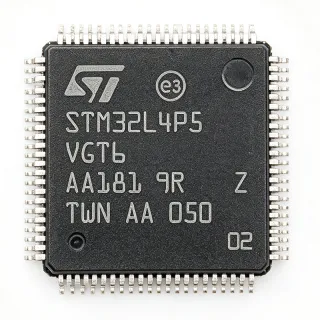
STM32F405VGT6J - 168MHz Cortex-M4 MCU, 1MB Flash | STMicro
Артикул: STM32F405VGT6J ✓ Активен| Кол-во | Цена за ед. | Итого |
|---|---|---|
| 1 | $12.5 | $12,50 |
| 10 | $11.25 | $112,50 |
| 100 | $9.8 | $980,00 |
| 500 | $8.95 | $4.475,00 |
| 1.000 | $8.1 | $8.100,00 |
STM32F405VGT6J Обзор
An ARM Cortex-M4 microcontroller is a 32-bit RISC processor core designed by ARM Ltd, typically used in embedded systems requiring deterministic real-time performance with low power consumption. The Cortex-M4 architecture sits between the Cortex-M3 (general-purpose MCU) and Cortex-M7 (highest-performance MCU) tiers, with added DSP extensions and an optional single-precision FPU. The STM32F4 family extends this hierarchy into STMicroelectronics' mainstream high-performance line, above the STM32F1 (Cortex-M3) and below the STM32F7 (Cortex-M7) and STM32H7 (Cortex-M7 dual-core). It is widely used for motor control, industrial automation, audio processing, and connected IoT devices.
Key features of the STM32F405VGT6J include 1 MB of embedded Flash memory, 192 KB of SRAM, an Adaptive Real-Time (ART) Accelerator that allows 0-wait-state execution from Flash memory at the full 168 MHz, a memory protection unit (MPU), and a rich set of peripherals including USB OTG full-speed and high-speed, CAN 2.0B, SDIO, FSMC, multiple USART/UART/SPI/I2C interfaces, and a 12-bit ADC. The 1.7 V to 3.6 V wide supply voltage range supports both 1.8 V and 3.3 V I/O domains with internal LDOs and a POR/PDR/PVD power-on-reset block.
Typical applications include industrial motor drives, three-phase inverters, PLCs, USB audio devices, barcode scanners, alarms, video intercoms, HVAC controllers, GPS trackers, and consumer wearables. The combination of DSP/FPU, large SRAM, USB HS, and Ethernet MAC (where present on pin-compatible F407 parts) makes this MCU well suited as a system controller.
When designing with this device, ensure the 100-LQFP PCB layout dedicates adequate copper to the exposed thermal pad for heat dissipation under sustained DSP load, and place the 4.7 uF VDD bypass capacitors as close as possible to each VDD/VDDA pin. Use ST-Link/V2-1 or a SEGGER J-Link for firmware debug; the on-chip DFU bootloader over USB FS allows field firmware updates without an external programmer.
This page synthesizes verified distributor pricing, pin-compatible STM32F405/407/415 drop-in alternatives, and practical design notes for high-performance Cortex-M4 designs that are not consolidated on the ST datasheet alone.
Аналоги без доработки для STM32F405VGT6J — тот же корпус, pin-to-pin совместимость. Компоненты в других корпусах, требующие переработки PCB, исключены.
Варианты в этой серии
Модели той же серии, совместимые без доработки с STM32F405VGT6J (тот же форм-фактор и посадочное место) — отличается по Core, Package, Communication Interfaces, Flash Memory, SRAM.
Инструмент быстрого сравнения — выберите альтернативные компоненты для сравнения бок о бок:
STM32F407VGT6
✅ Прямая замена ⚠️ Характеристики не проверены✓ В наличии
$7.55 / шт.
Открыть даташит →STM32F405VGT6
✅ Прямая замена ⚠️ Характеристики не проверены✓ В наличии
$8.1 / шт.
Открыть даташит →STM32F405VGT6J Максимальные параметры и электрические характеристики
| Core | ARM Cortex-M4 with FPU + DSP instructions |
| Core Architecture | ARM 32-bit RISC |
| Максимальная тактовая частота | 168 MHz |
| Performance | 210 DMIPS / 1.25 DMIPS/MHz (Dhrystone 2.1) |
| Program Memory | 1 MB Flash (1M x 8) |
| SRAM | 192 KB |
| Operating Voltage Range | 1.8 V to 3.6 V (typical: 2.0 V to 3.6 V) |
| Supply Voltage Min | 1.7 V |
| I/O Pins | 82 (on 100-LQFP) |
| Корпус | 100-LQFP (14x14 mm) |
| Тип монтажа | Surface Mount |
| Диапазон рабочих температур | -40C to +85C (industrial grade 'J' suffix) |
| Communication Interfaces | USB OTG FS + HS, CAN 2.0B x2, UART/USART x6, SPI x3, I2C x3, SDIO, FSMC |
| ADC | 12-bit, up to 2.4 MSPS, 16+ channels |
| DAC | 12-bit, 2 channels |
| Timers | Advanced-control x2, General-purpose x10, Basic x2, SysTick, Watchdog x2 |
| Статус RoHS | Compliant |
| Lead-Free / Halogen-Free | Yes (lead-free finish); halogen-free status per datasheet |
Конфигурация выводов STM32F405VGT6J
| Контакт 1 | PE2 — General-purpose I/O; TRACECLK on some debuggers |
| Контакт 2 | PE3 — General-purpose I/O; TRACED0 trace data |
| Контакт 3 | PE4 — General-purpose I/O; TRACED1 trace data |
| Контакт 4 | PE5 — General-purpose I/O; TRACED2 trace data |
| Контакт 5 | PE6 — General-purpose I/O; TRACED3 trace data |
| Контакт 6 | VBAT — Backup battery supply input for RTC/BACKUP SRAM |
| Контакт 7 | PC13 — GPIO; Tamper-RTC (PC13-TAMPER-RTC) |
| Контакт 8 | PC14 — GPIO; OSC32_IN (32.768 kHz LSE crystal) |
| Контакт 9 | PC15 — GPIO; OSC32_OUT (32.768 kHz LSE crystal) |
| Контакт 10 | VSS — Ground |
| Контакт 11 | VDD — Main digital supply (1.7-3.6 V); bypass with 100 nF + 4.7 uF |
| Контакт 12 | PH0 — GPIO; OSC_IN (HSE crystal) |
| Контакт 13 | PH1 — GPIO; OSC_OUT (HSE crystal) |
| Контакт 14 | NRST — Active-low reset input (must be pulled up) |
| Контакт 15 | PC0 — GPIO; ADC1_IN10 |
| Контакт 16 | PC1 — GPIO; ADC1_IN11 |
| Контакт 17 | PC2 — GPIO; ADC1_IN12 |
| Контакт 18 | PC3 — GPIO; ADC1_IN13 |
| Контакт 19 | VSSA — Analog ground |
| Контакт 20 | VDDA — Analog supply (1.8/3.3 V); tie to VDD with ferrite per datasheet |
| Контакт 21 | PA0 — GPIO; WKUP, ADC1_IN0, TIM5_CH1 |
| Контакт 22 | PA1 — GPIO; ADC1_IN1, TIM5_CH2 |
| Контакт 23 | PA2 — GPIO; USART2_TX, TIM5_CH3, ADC1_IN2 |
| Контакт 24 | PA3 — GPIO; USART2_RX, TIM5_CH4, ADC1_IN3 |
| Контакт 25 | VSS — Ground |
| Контакт 26 | VDD — Main digital supply |
| Контакт 27 | PA4 — GPIO; SPI1_NSS/USART2_CK, ADC1_IN4, DAC1_OUT |
| Контакт 28 | PA5 — GPIO; SPI1_SCK, ADC1_IN5, DAC2_OUT |
| Контакт 29 | PA6 — GPIO; SPI1_MISO, TIM13_CH1, ADC1_IN6 |
| Контакт 30 | PA7 — GPIO; SPI1_MOSI, TIM14_CH1, ADC1_IN7 |
| Контакт 31 | PC4 — GPIO; ADC1_IN14 |
| Контакт 32 | PC5 — GPIO; ADC1_IN15 |
| Контакт 33 | PB0 — GPIO; TIM3_CH3, ADC1_IN8, PWM_OUT |
| Контакт 34 | PB1 — GPIO; TIM3_CH4, ADC1_IN9 |
| Контакт 35 | PB2 — GPIO; BOOT1 alternate function |
| Контакт 36 | PE7 — GPIO; TIM1_ETR |
| Контакт 37 | PE8 — GPIO; TIM1_CH1N (complementary PWM) |
| Контакт 38 | PE9 — GPIO; TIM1_CH1 (PWM) |
| Контакт 39 | PE10 — GPIO; TIM1_CH2N |
| Контакт 40 | PE11 — GPIO; TIM1_CH2 |
| Контакт 41 | PE12 — GPIO; TIM1_CH3N |
| Контакт 42 | PE13 — GPIO; TIM1_CH3 |
| Контакт 43 | PE14 — GPIO; TIM1_CH4 |
| Контакт 44 | PE15 — GPIO; TIM1_BKIN |
| Контакт 45 | PB10 — GPIO; I2C2_SCL, USART3_TX |
| Контакт 46 | PB11 — GPIO; I2C2_SDA, USART3_RX |
| Контакт 47 | VSS — Ground |
| Контакт 48 | VDD — Main digital supply |
| Контакт 49 | PB12 — GPIO; SPI2_NSS, I2S2_WS, USART3_CK |
| Контакт 50 | PB13 — GPIO; SPI2_SCK, I2S2_CK, USART3_CTS |
| Контакт 51 | PB14 — GPIO; SPI2_MISO, USART3_RTS |
| Контакт 52 | PB15 — GPIO; SPI2_MOSI, I2S2_SD |
| Контакт 53 | PD8 — GPIO; USART3_TX, FSMC_D13 |
| Контакт 54 | PD9 — GPIO; USART3_RX, FSMC_D14 |
| Контакт 55 | PD10 — GPIO; FSMC_D15 |
| Контакт 56 | PD11 — GPIO; USART3_CTS, FSMC_A16 (F407 only) |
| Контакт 57 | PD12 — GPIO; TIM4_CH1, FSMC_A17 (F407 only) |
| Контакт 58 | PD13 — GPIO; TIM4_CH2, FSMC_A18 (F407 only) |
| Контакт 59 | VSS — Ground |
| Контакт 60 | VDD — Main digital supply |
| Контакт 61 | PD14 — GPIO; TIM4_CH3, FSMC_D0 |
| Контакт 62 | PD15 — GPIO; TIM4_CH4, FSMC_D1 |
| Контакт 63 | PC6 — GPIO; I2S2_MCK, TIM3_CH1 |
| Контакт 64 | PC7 — GPIO; I2S3_MCK, TIM3_CH2 |
| Контакт 65 | PC8 — GPIO; TIM3_CH3, SDIO_D0 |
| Контакт 66 | PC9 — GPIO; TIM3_CH4, SDIO_D1 |
| Контакт 67 | PA8 — GPIO; TIM1_CH1, USART1_CK, MCO1 |
| Контакт 68 | PA9 — GPIO; USART1_TX, TIM1_CH2 |
| Контакт 69 | PA10 — GPIO; USART1_RX, TIM1_CH3 |
| Контакт 70 | PA11 — GPIO; USB OTG FS D-, CAN1_RX |
| Контакт 71 | PA12 — GPIO; USB OTG FS D+, CAN1_TX |
| Контакт 72 | PA13 — GPIO; JTMS / SWDIO debug |
| Контакт 73 | VCAP_1 — Internal LDO cap; tie 2.2 uF/100 nF to VSS per datasheet |
| Контакт 74 | VSS — Ground |
| Контакт 75 | VDD — Main digital supply |
| Контакт 76 | PA14 — GPIO; JTCK / SWCLK debug |
| Контакт 77 | PA15 — GPIO; JTDI; SPI3_NSS, I2S3_WS |
| Контакт 78 | PC10 — GPIO; UART4_TX, SDIO_D2, SPI3_SCK |
| Контакт 79 | PC11 — GPIO; UART4_RX, SDIO_D3, SPI3_MISO |
| Контакт 80 | PC12 — GPIO; UART5_TX, SDIO_CK |
| Контакт 81 | PD0 — GPIO; CAN1_RX, FSMC_D2 |
| Контакт 82 | PD1 — GPIO; CAN1_TX, FSMC_D3 |
| Контакт 83 | PD2 — GPIO; SDIO_CMD, TIM3_ETR |
| Контакт 84 | PD3 — GPIO; USART2_CTS, FSMC_CLK |
| Контакт 85 | PD4 — GPIO; USART2_RTS, FSMC_NOE |
| Контакт 86 | PD5 — GPIO; USART2_TX, FSMC_NWE |
| Контакт 87 | PD6 — GPIO; USART2_RX, FSMC_NWAIT |
| Контакт 88 | PD7 — GPIO; USART2_CK, FSMC_NCE2 |
| Контакт 89 | PB3 — GPIO; JTDO; SPI3_SCK, I2S3_CK |
| Контакт 90 | PB4 — GPIO; NJTRST; SPI3_MISO |
| Контакт 91 | PB5 — GPIO; SPI3_MOSI, I2S3_SD, CAN2_RX |
| Контакт 92 | PB6 — GPIO; I2C1_SCL, USART1_TX, CAN2_TX |
| Контакт 93 | PB7 — GPIO; I2C1_SDA, USART1_RX |
| Контакт 94 | BOOT0 — Boot mode select input (must be low for Flash boot) |
| Контакт 95 | PB8 — GPIO; TIM4_CH3, SDIO_D4, I2C1_SCL |
| Контакт 96 | PB9 — GPIO; TIM4_CH4, SDIO_D5, I2C1_SDA |
| Контакт 97 | PE0 — GPIO; TIM4_ETR, FSMC_NBL0 |
| Контакт 98 | PE1 — GPIO; FSMC_NBL1 |
| Контакт 99 | VSS — Ground |
| Контакт 100 | VDD — Main digital supply |
Типичное применение
STM32F405VGT6J подходит для 6 применениеs: Industrial Motor Control and Drives, USB Audio and Consumer Multimedia Devices, Industrial IoT Gateways and PLCs, Barcode Scanners and Industrial Imaging, HVAC Controllers and Building Automation, Wearables and Battery-Powered Smart Devices.
Industrial Motor Control and Drives
The STM32F405VGT6J's 168 MHz Cortex-M4 with FPU and DSP extensions is well matched to FOC (field-oriented control) of 3-phase PMSM, BLDC, and stepper motors, plus PFC stages. The two advanced-control timers (TIM1, TIM8) generate complementary PWM with programmable dead-time, while the 12-bit 2.4 MSPS ADC samples phase currents and back-EMF at the PWM cycle rate. The 192 KB SRAM holds controller state plus enough headroom for sensorless observers (Sliding-Mode, MRAS) and second-stage filtering. Per the ST datasheet typical-application block diagrams, the same LQFP-100 design can run both an industrial servo loop and a CANopen/DeviceNet upper layer on the dual CAN 2.0B controllers. Reference companions: STM32F405VGT6J driver board + external 6-MOSFET gate drivers (e.g. STGIPN3H60 or STDRIVE101 companion).
Рекомендуется
USB Audio and Consumer Multimedia Devices
The integrated USB OTG full-speed + high-speed with on-chip HS PHY makes STM32F405VGT6J a fit for USB speakerphones, USB audio cards, USB headphones, and professional USB audio interfaces. The Cortex-M4 + DSP SIMD instructions handle S/PDIF pass-through and basic DSP filters (EQ, dynamics) while the I2S peripherals connect to external DAC/ADC codecs. The 192 KB SRAM is sufficient for 4-channel 48 kHz audio buffers plus firmware. Per the ST application note for USB audio class 2.0, the part enumerates as a USB Audio device without external crystal beyond the standard 25.2349 ppm quartz. Recommended companions: WM8960CGEFL/RV audio codec (XAIPART-listed); CS43L22 DAC amplifier.
Рекомендуется
Industrial IoT Gateways and PLCs
The dual CAN 2.0B (CANopen, DeviceNet) plus 10/100 Ethernet on pin-compatible F407 parts, plus USB, USART, and UARTs make STM32F405VGT6J strong as an industrial IoT edge gateway controller. The 1 MB Flash holds full Modbus RTU/TCP, MQTT, CoAP, and TLS 1.2 client stacks; the 192 KB SRAM holds TLS handshake buffers and JSON parsing workspaces. The FSMC lets it extend with external SRAM or NOR Flash when firmware grows. Per the ST datasheet peripheral mux tables, a single LQFP-100 pinout can drive both Ethernet MAC (with a 25 MHz PHY reference like LAN8720) and an SDIO Wi-Fi/BT module. Recommended companions: KSZ9477STXI managed Ethernet switch; ESP32 wireless companion (external).
Рекомендуется
Barcode Scanners and Industrial Imaging
The STM32F405VGT6J's DCMI camera interface plus DMA-driven image pipelines supports 1.3 MP barcode/QR scanners and basic industrial machine-vision tasks. The ART-accelerated 168 MHz CPU decodes Code-128, QR, DataMatrix, and PDF417 in firmware with the help of the DSP extensions for Sobel/edge-detection preprocessing. The 192 KB SRAM holds a full image frame buffer plus decoded data while the LCD controller (LTDC not on this SKU, but FSMC drives parallel displays) shows results. Per ST reference designs for handheld scanners, the part typically runs a 1.5-inch to 2.4-inch TFT plus a 1D/2D imager module. Recommended companions: AMS TSL1401R-LS linear CCD; ILI9341 TFT controller.
Рекомендуется
HVAC Controllers and Building Automation
The wide 1.7 V to 3.6 V supply and -40C to +85C industrial temp range plus Cortex-M4 math power make STM32F405VGT6J apt for multi-zone HVAC controllers with on-device control loops. Two advanced-control timers run BLDC fan motors, while the FPU runs PI/PID control algorithms at 1 kHz sample rates. SDIO connects to Wi-Fi/BT modules for cloud linkage; CAN interfaces to building automation backplanes (BACnet MS/TP, CANopen); FSMC controls parallel character/graphics LCDs. Per the ST datasheet peripheral sharing tables, the LQFP-100 pinout can simultaneously drive a 7-segment or TFT user interface plus triac outputs for AC loads. Recommended companions: MCP2562-E/SN CAN transceiver; zero-cross detector MOC3021.
Рекомендуется
Wearables and Battery-Powered Smart Devices
For consumer wearables that need Cortex-M4 compute but acceptable battery life, the STM32F405VGT6J is at the edge of suit; the Lower-power STM32L4 or STM32U5 is recommended for sub-50 uA average power budgets. The extensive STM32F4 ecosystem (CubeMX, TouchGFX for graphics, LoRa, BLE stacks) makes F405 attractive for connected watches, rings, and GPS trackers where battery is rechargeable. The 1 MB Flash holds full BLE stack + GUI/TouchGFX assets; the 192 KB SRAM supports display buffers for small TFTs. Per the datasheet, the Stop/Standby modes drop current to a few uA while RTC holds time, supporting weeks-months of stand-by. Recommended companions: SX1262 LoRa transceiver; 1.3-inch OLED displays.
Рекомендуется
Сводка рекомендуемых товаров
Справочные инженерные данные для STM32F405VGT6J — сравнение, рекомендации по проектированию и информация о соответствии.
Руководство по выбору
Сравнение с аналогами
| Параметр | Этот товар | STM32F407VGT6 | STM32F405VGT6 |
|---|---|---|---|
| Brand | STMicroelectronics | STMicroelectronics (same family) | STMicroelectronics (same die, T6 variant) |
| Package | 100-LQFP (14x14 mm) | 100-LQFP (14x14 mm) - same | 100-LQFP (14x14 mm) - same |
| Core | ARM Cortex-M4 + FPU + DSP | ARM Cortex-M4 + FPU + DSP (same) | ARM Cortex-M4 + FPU + DSP (same) |
| Max Clock Frequency | 168 MHz | 168 MHz | 168 MHz |
| Flash Memory | 1 MB | 1 MB | 1 MB |
| SRAM | 192 KB | 192 KB | 192 KB |
| Ethernet MAC | No (F405 family) | Yes (10/100 MII/RMII) | No |
| USB OTG FS/HS | Yes (FS + HS on-chip PHY) | Yes (FS + HS) | Yes (FS + HS) |
| Temperature Grade | -40C to +85C (industrial 'J') | -40C to +85C | -40C to +85C |
Ключевые отличия
- Industrial -40C to +85C ('J' suffix) explicitly guaranteed with shipped test data (против STM32F405VGT6 (T6, -40C to +85C, broader distribution channel))
- Same LQFP-100 footprint as STM32F407 family enabling in-family upgrade path (против STM32F103VGT6 (same LQFP-100 but Cortex-M3, 72 MHz))
- ART Accelerator + 0-wait-state Flash execution at 168 MHz (против Kinetis MK60DN512VLQ10 (Cortex-M4 at 100 MHz, 3-wait Flash))
Заметки по проектированию
Place a 100 nF (X7R 0402/0603) plus a 4.7 uF ceramic bulk capacitor within 1-2 mm of each VDD/VDDA ball as the ST datasheet recommends. Tie VCAP_1 to VSS via a 2.2 uF X5R capacitor of low ESR; insufficient VCAP_1 capacitance prevents the internal 1.2 V regulator from stabilizing and the core resets. For VDDA, use a ferrite-bead or simple LC filter from VDD; some noise-sensitive ADC/DAC designs add a separate low-noise LDO (e.g. ADM7150) for VDDA.
Estimated: at 3.3 V supply, full 168 MHz Dhrystone workload (~85 mA core current per datasheet), the LQFP-100's theta_JA of ~50 C/W on a 2-layer FR4 PCB would push the junction to ~74 C (50 * 0.085 * 1 + 25 C ambient). For sustained 100% DSP or motor-control duty cycles, route the bottom ground plane beneath the package and consider 4-layer stack-up with continuous ground planes to lower theta_JA to 30-35 C/W. Free-air forced convection is recommended for environments above +60 C ambient.
Keep high-speed USB DP/DM, HS PHY pins, and the HSE/LSE crystal traces short and symmetric. Reference ST application note AN2867 for oscillator PCB layout guidelines. For SDRAM/NOR over FSMC, use trace-length matching within +/- 2 mm on the 16-bit bus to avoid timing skew. The DCMI parallel camera bus should be guarded by 8b/10b length matching if image quality drops, and the SDIO bus should have 33 ohm series termination at the driver.
Do not confuse the F405 (no Ethernet) with F407 (10/100 Ethernet MAC) at PCB bring-up - if a board ships with F405 in a design that needs Ethernet, the RMII/MII pins will appear silent. Watch for the 'J' suffix: STM32F405VGT6J is industrial -40C to +85C, while the plain T6 is also industrial but different mass-availability channel per distributor. BOOT0 must be pulled low for normal Flash boot; lifting it high selects the system memory bootloader for factory programming.
Differential pair layout for USB DP/DM must keep 90 ohm impedance and 0.5-1 mm spacing; the HS PHY clock (60 MHz) must be routed over continuous ground plane. For ADC circuits, use a Kelvin connection to AGND with the analog ground shaped by the analog-current return path (avoid splitting GND; instead, make one continuous ground). Per the ST datasheet, DAC output impedance is ~3.3 kohm and needs op-amp buffers to drive low-impedance loads without 30%+ linearity loss.
Информация о соответствии
Per STMicroelectronics product environmental documentation: RoHS compliant (2011/65/EU), lead-free finish, REACH compliant, China RoHS 2 compliant. Industrial-grade temperature -40C to +85C (J suffix). No formal AEC-Q100 certification - refer to AEC-Q100-qualified members of the F4 family if automotive qualification is required. ST reports CMRT/EMRT filings for conflict minerals compliance.